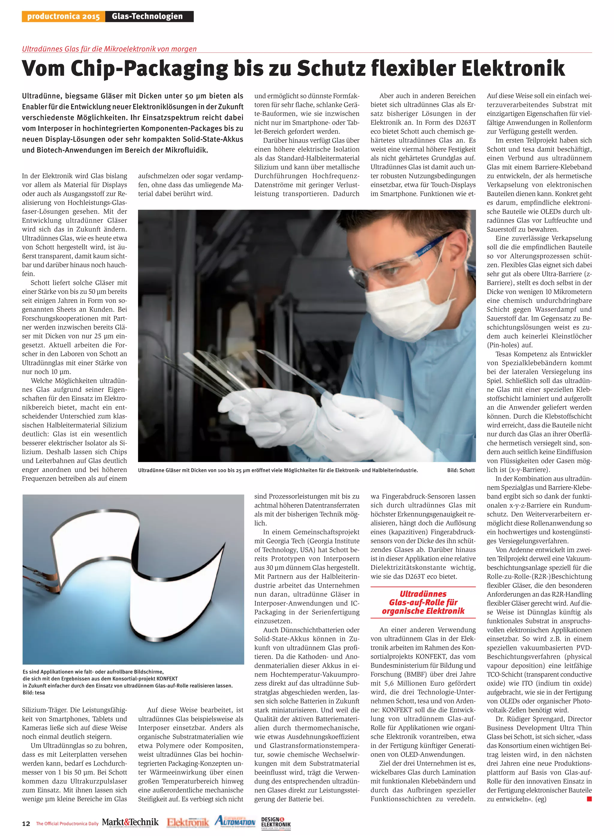
productronica's official daily features information about trends and topics directly from the world's leading trade fair for electronics manufacturing.
______________________________
Die offizielle Tageszeitung der productronica informiert über Themen und Trends direkt von der Weltleitmesse der Elektronikfertigung.
1. productronica celebrates anniversary
Plenty of innovations
The world's leading trade fair for elec-
tronics development and production sets
new standards with a number of innova-
tions.
Besides its new cluster concept, the pre-
miere of a new award and a new forum
concept, for the first time ever, IT2Industry,
the trade fair and open conference for in-
telligent, digitally networked working en-
vironments, takes place at the same time
as productronica.
This year's focus topics are industrial
electronics, automotive electronics and
PCB & EMS. They will each have their own
theme day including a number of lectures
and roundtable discussions with represen-
tatives from the commercial and industrial
sectors. ■
gungsmaschinen aufwerten, verein-
fachen und verbessern können, sind
vielfältig: »Wir erleben damit gerade
die Evolution vom fest eingebauten
Touch-Panel-Display zur Bedienung
mit Tablet. Fernwartung wird erheb-
lich erleichtert«, so Maiser. Wird das
Tablet an verschiedene Teile einer
Maschine gehalten, zeigt das Pro-
gramm sofort die passende Bedie-
nungsanleitung oder Arbeitsanwei-
sung an – das Benutzerhandbuch
kann im Schrank bleiben. (zü) n
productronica’s special show
Augmented and virtual reality
Electronics.Production.Augmented. – that is the motto
of a special show that is part of productronica. The
world's leading trade fair for electronics development
and production will focus on the hot topic of Industry
4.0 from a new perspective: visitors will experience
the hidden processes machines and workpieces nego-
tiate in production and how workers profit from In-
dustry 4.0 – with the help of augmented and virtual
reality on five electronics production machines.
Industry 4.0 poses great challenges to electronics
production, but it also has its advantages. The diffe-
rent use cases of the adaptive automation technology
as well as the exact procedures on hardware and soft-
ware side are often seen as too abstract by workers
on the line. That is why productronica and VDMA
Productronic have come up with a new special show
for the 2015 fair. ■
As long as it‘s innovative
First productronica
innovation award
Innovative products and manufacturing
techniques must satisfy very clear criteria
to have a chance at the first productronica
innovation award: They must be techno-
logically innovative or economical, have a
brand new design or be easy to integrate
into systems. The productronica innova-
tion award is the first independent award
in the electronics production industry and
will be bestowed by productronica. The
world‘s leading trade fair is now giving all
companies in the industry a chance to sub-
mit their innovations for the award. ■
Industrie 4.0 visuell erleben
productronica mit
Augmented und Virtual Reality
Electronics.Production.Augmen-
ted. – unter dieses Motto stellt
die productronica ihre Sonder-
schau aufder diesjährigen Mes-
se und zeigt auf diese Weise
auchdasTrendthema”Industrie
4.0” unter einem neuen Aspekt.
Die productronica und der VDMA
Productronic haben sich für die Son-
derschau etwas Besonderes ausge-
dacht: Mit Hilfe von Augmented und
Virtual Reality werden an fünf ver-
schiedenen Elektronikfertigungsma-
schinen unterschiedliche Einsatz-
szenarien von Industrie 4.0 visuali-
siert.
»Wir wollen zeigen, wie Indus-
trie 4.0 das Leben derjenigen er-
leichtern kann, die tagtäglich mit
den Maschinen umgehen«, sagt
Christian Rocke, Projektleiter pro-
ductronica. »Das ist nicht nur für
unsere Besucher interessant, son-
Mit einigen Neuerungen präsen-
tiert sich die productronica im
Jubiläumsjahr: Eine neue Struk-
tur soll die Wertschöpfungskette
der Elektronikfertigung wider-
spiegeln. So wurden die bislang
19 unterschiedlichen Segmente
in eine neue Struktur mit fünf
Clustern gegliedert:
• PCB & EMS
• SMT
• Semiconductor
• Cables, Coils & Hybrid
• Future Market
productronica 2015
Zum 40. in neuem Kleid
dern bietet gleichzeitig einen span-
nenden Mehrwert für unsere Aus-
steller der Sonderschau.«
Die besten Innovationen
visuell erleben
Wie sieht das Innenleben der Ma-
schine aus? Was passiert gerade in
unzugänglichen Bereichen der Ma-
schine? Welche Anweisungen gibt
die Maschine dem Werkstück? Das
sind Fragen, deren Antworten sich
mit Hilfe von Augmented und Virtu-
al Reality visualisieren lassen. »Die
Weiterentwicklung der Mensch-Ma-
schine-Schnittstelle ist seit jeher ein
Schlüssel für den Erfolg des deut-
schen Maschinenbaus. Der Werker
will nicht nur eine bedienerfreund-
liche, sondern auch eine verständli-
che Maschine«, erklärt Dr. Eric Mai-
ser, Geschäftsführung VDMA Pro-
ductronic. Die Anwendungen für
Industrie 4.0, die Elektronikferti-
Day 1
3. The Official Productronica Daily 3
productronica 2015 Messtechnik
Wie geht es weiter nach der Integration von Hameg Instruments in den Rohde&Schwarz-Konzern?
»Die Hameg-Produkte
leben als Value Instruments weiter«
VoreinigenWochengabRohde&Schwarzbekannt,dieTochtergesellschaftHameg
Instruments vollständig in den Konzern zu integrieren. Was wird nun aus der Tra-
ditionsmarkeHameg?UndwelchePläneverfolgtRohde&SchwarzmitdenHameg-
Produkten? André Vander Stichelen, Vice President Value Instruments Sales von
Rohde & Schwarz und Geschäftsführer von Hameg, erklärt die Hintergründe.
Markt&Technik: Für viele Marktbeobach-
ter kam die Meldung der vollständigen
IntegrationHamegsindieRohde&Schwarz-
Strukturen nicht ganz unerwartet. Wie ist
der Stand der Dinge?
André Vander Stichelen: Wir sind mitten im
Prozess der Integration. Alle Mitarbeiter,
Kunden und Lieferanten sind informiert. Ziel
ist es, die Hameg GmbH im laufenden
Rohde&Schwarz-Geschäftsjahr – also bis
spätestens 30. Juni 2016 – aufzulösen.
Was ändert sich für die Kunden?
Wir hatten die Vertriebswege beider Unter-
nehmensteile ja bereits vor einiger Zeit zu-
sammengelegt. Insofern können Kunden die
Produkte weiterhin über die ihnen bekann-
ten Kanäle wie Katalog- und Fachdistributo-
ren und über das Rohde & Schwarz Direct
Sales Team beziehen. Die Ansprechpartner
bleiben die gleichen – inklusive des Produkt-
managements. Die Hameg.com-Internetseite
und die Hameg-Support-Hotline werden
nahtlos auf Rohde & Schwarz umgeleitet.
Was wird aus der Marke Hameg?
Hameg als eigenständige Marke gibt es nicht
mehr. Die ehemaligen Hameg-Produkte sind
mittlerweile komplett in den Value-Instru-
ments-Bereich von Rohde & Schwarz einge-
gangen und bilden dort einen essentiellen
Bestandteil des Portfolios, das wir auch kon-
tinuierlich weiter ausbauen werden.
Hameg galt lange Zeit als »Billigmarke«
für Bastler und Hobby-Elektroniker. Er-
schrickt diese Klientel nicht vor dem gro-
ßen Namen Rohde & Schwarz?
Seit der Übernahme durch Rohde & Schwarz
2005 hat sich das Image der Hameg-Produk-
te massiv verändert. Heute adressieren wir
mit den Value Instruments sowohl den pri-
vaten Anwender als auch das Einstiegsseg-
ment des professionellen Nutzers. Wir ha-
ben bereits eine große installierte Basis im
Ausbildungsbereich, weil dort günstige Pro-
dukte gefragt sind. Aber wir freuen uns na-
türlich über jeden einzelnen Kunden – egal
ob Hobby-Elektroniker oder professioneller
Entwickler beziehungsweise Ingenieur.
Ist es nicht gefährlich, eine seit Jahrzehn-
ten so fest etablierte Marke komplett vom
Markt zu nehmen?
Nun, wir hier in Deutschland sind natürlich
mit dieser Marke groß geworden. Doch der
Name Hameg ist vorwiegend in Zentraleuro-
pa bekannt, in anderen Teilen der Welt eher
weniger. Rohde & Schwarz hingegen ist global
etabliert und steht für qualitativ hochwertige
Messtechnik. Um diese Bekanntheit auch au-
ßerhalb Europas für die Hameg-Produkte zu
nutzen, hatten wir den langsamen Übergang
der Marken durchgeführt, vom Hameg- über
das duale Label bis hin zum alleinigen
Rohde&Schwarz-Label und der Integration
der Hameg-Produkte in den Value-Instru-
ments-Bereich von Rohde & Schwarz. Hin-
sichtlich des Markennamens war der Über-
gang also bereits vor einiger Zeit erfolgt.
Was verspricht sich Rohde & Schwarz da-
von?
Rohde & Schwarz wird noch nicht ausrei-
chend mit dem Einstiegsbereich assoziiert.
Unser Name steht für Attribute wie Qualität
und Verlässlichkeit. Dennoch liegt immer
noch der Schatten »teuer« über uns, auch
wenn das bei genauem Hinsehen und Ver-
gleichen oft gar nicht der Fall ist. Dieses Bild
wollen wir mit den Value Instruments korri-
gieren. Dabei wird die Integration des Ha-
meg-Portfolios sicher hilfreich sein. Letztend-
lich läuft es darauf hinaus: Wir wollen in
allen Segmenten – von der Einstiegs- über die
Mittelklasse bis hin zu den High-end-Geräten
– hochqualitative Produkte zu marktfähigen
Preisen anbieten und damit auch im Be-
wusstsein der Kunden verankert sein.
Erwarten Sie einen Zuwachs an Marktan-
teilen?
Das hängt nicht allein von der Preispolitik
ab. Nehmen wir das Beispiel Oszilloskope:
Rohde & Schwarz ist 2010 in einen Markt
eingetreten, der nur unwesentlich wächst.
Hier kann man Marktanteile also nur durch
Verdrängung gewinnen. Das wiederum ge-
lingt nur, wenn man mit technologisch aus-
gereiften und exakt auf die Anforderungen
der Kunden angepassten Produkten aufwar-
tet. Genau das haben wir gemacht – von
anfangs zwei Produkten haben wir unser
Portfolio massiv erweitert und bieten jetzt in
drei Scope-Serien Modelle mit über zehn
verschiedenen Typen an, dazu noch eine
Vielzahl an Applikationspaketen und Zube-
hör. In dieser Art und Weise werden wir auch
das Value-Instruments-Portfolio kontinuier-
lich ausbauen und so hoffentlich Marktan-
teile für uns gewinnen können.
Welche Strategien verfolgen Sie dabei?
Rohde & Schwarz pflegt traditionell eine sehr
langfristige Ausrichtung. Um beim Beispiel
der Oszilloskope zu bleiben: Als wir vor fünf
Jahren in den Markt eingetreten sind, sind
unsere Mitbewerber nicht gerade in Panik
verfallen – zu klein war unser Portfolio und
zu unbekannt waren wir in diesem Markt.
Das hat sich geändert: Mittlerweile ist Rohde
& Schwarz immer dabei, wenn es um Bench-
marking geht. Plakativ ausgedrückt: Liefen
wir früher völlig unter dem Radarschirm der
Mitbewerber, so sind wir heute mittendrin.
Dennoch ist uns schon klar, dass man in fünf
Jahren nicht das schaffen kann, was andere
in 50 Jahren aufgebaut haben. Gleiches gilt
für die Value Instruments: Auch hier gibt es
schon bekannte Anbieter, die die Spielregeln
in diesem Markt festgesetzt haben. Die müs-
sen wir befolgen, doch wir sind auf dem
besten Weg, uns auch hier einen Namen zu
machen. Wir bleiben dran, kontinuierlich
und ausdauernd, so wie man Rohde &
Schwarz nun mal kennt.
Was sind Ihre nächsten Ziele?
Das übergeordnete Ziel heißt natürlich
Wachstum – organisch und durch Zukäufe.
Wir wollen neue Märkte erschließen und
unsere Internationalisierung vorantreiben.
Dazu müssen wir unser Händlernetzwerk
ausbauen und dabei vielleicht auch mal die
ausgetretenen Pfade verlassen. Hier kommt
uns unsere Unabhängigkeit sehr zugute:
Was man auf dem Markt nicht findet, kön-
nen wir aus eigener Finanzkraft schaffen.
An was denken Sie dabei konkret?
Nun, wir sind offen für alles …
Das Interview führte Nicole Wörner
André Vander Stichelen,
Rohde & Schwarz / Hameg Instruments:
»Rohde & Schwarz wird noch nicht ausreichend
mit dem Einstiegsbereich assoziiert. Es liegt
immer noch der Schatten ’teuer‘ über uns.
Dieses Bild wollen wir mit den Value Instruments
korrigieren.«
productronica and electronica are not just
successful in Germany: Their spin-off
events have also met with a great deal of
success. The trade fairs in China and India
are established platforms for the internati-
onal electronics industry and are among the
leading events of their kind in in their re-
gion. Increasing growth of the electronics
market is reflected by the number of com-
panies that participate in the fairs. electro-
nica China and productronica China do an
impressive job of proving that fact: A total
of 1,006 exhibitors from 28 countries and
regions gathered to showcase their latest
technologies and services and 55,365 visi-
tors participated at this year’s show. Also,
in India the two shows, electronica India
and productronica India, ended with an
outstanding result: 352 exhibitors, repre-
senting 634 companies, showcasing their
products, solutions and services to 15,435
visitors. Trade-fair dates at a glance:
• electronica China and productronica
China: March 15 – 17, 2016, Shanghai
New International Expo Center (SNIEC)
• electronica India and productronica
India: September 21 – 23, 2016, BIEC,
Bangalore
Trade fairs in China and India
Global network of technology fairs
4. 4 The Official Productronica Daily
Liebe Leser,
ein Leben ohne Smartphones und Tablets ist
heute gar nicht mehr vorstellbar. Auch die
productronica hat in den letzten 40 Jahren
dazu beigetragen, dass es diese Produkte heu-
te gibt, denn nur die stetige Weiterentwick-
lung des Maschinenbaus und der Elektronik-
fertigung hat die Produktion solch komplexer
Elektronik ermöglicht.
Inzwischen sind die smarten Helferlein
auch in die Produktion vorgedrungen: Es gibt
inzwischen für alles eine App – auch für Ma-
nufacturing Execution Systeme, die im Zuge
der Industrie 4.0 Dreh- und Angelpunkt in der
Prozesssteuerung und Datenanalyse sein wer-
den. Nicht nur der Fertigungsleiter kann die
Fertigungsdaten von unterwegs aus einsehen.
Künftig wird auch der Werker über mobile
Endgeräte immer mehr in die „Smartisierung“
der Fertigung eingebunden werden, etwa um
über Augmented und Virtual Reality Software
den Wartungszustand der Maschinen von au-
ßen im Blick zu haben.
Der Industrie-4.0-Gedanke ist im Shop
Floor der Elektronikfertigungen angekom-
men, wie sich beim Rundgang über die pro-
ductronica unschwer erkennen lässt: ange-
fangen bei sich selbst regulierenden SMT-
Linien über den automatischen Material-
nachschub bis hin zur Software, die die Ver-
netzung über Werks- und Unternehmens-
grenzen hinweg ermöglicht. Letzteres ist al-
lerdings noch die Ausnahme.
Industrie 4.0 in der Elektronikfertigung ist
Stand heute in den meisten Fällen noch auf
die interne Vernetzung begrenzt und darauf
ausgerichtet, interne Prozesse zu optimieren.
Extern und unternehmensübergreifend sind
bislang die wenigsten Fertigungen vernetzt.
Dafür fehlen schlichtweg oft noch die „End-
to-End“-Geschäftsmodelle. Denn wer inves-
tiert, möchte sichergehen, dass sich die Inves-
tition auch „monetarisieren“ lässt. Im Ideal-
fall sähe die Industrie-4.0-Produktion zum
Beispiel so aus: Ein Kunde bestellt sein indi-
viduell konfiguriertes Produkt in Losgröße 1
beim Händler, die Bestellung gelangt direkt in
das ERP-System des Fertigungsbetriebes und
wird dort als Box-Built-System nach allen
„smarten“ Regeln der Kunst produziert. An-
schließend wird es direkt an den Endkunden
ausgeliefert. In der Endausbaustufe wäre das
jedenfalls ein sehr „smarter“ Weg, um die
Lieferkette effizienter zu gestalten.
Die Geschäftsmodelle werden sich aus
den Anforderungen des Marktes entwickeln
und nicht umgekehrt. Wer dann vorne mit-
spielen möchte, sollte aber schon jetzt die
Weiche stellen. Die productronica bietet als
„Showroom“ jedenfalls einen guten Überblick
zu den Möglichkeiten der Industrie 4.0 im
Shop Floor. In diesem Sinne wünsche ich Ih-
nen eine spannende Messe!
Ihre Karin Zühlke,
Redaktion Markt&Technik
Showroom für den
Industrie 4.0 Shop Floor
Editorial»
Karin Zühlke
E-Mail: KZühlke@markt-technik
Showroom for Industry 4.0
on the Shop floor
Dear reader,
One can hardly imagine life today without
Smartphones or Tablets. In the meantime
these smart little helpers have even penetra-
ted the – previously regarded as rather down-
to-earth – production-line: Today there is an
app for everything – even for Manufacturing
Execution Systems that, in the wake of Indus-
try 4.0, will become the lynchpin for Process
Control and Data Analysis. Thus, it’s not on-
ly the Production Manager who can easily
check on manufacturing data while on the
move. In future, even the shop floor worker
will become more and more involved in the
"Smartization" of production via mobile de-
vices, to monitor, for example, processes on
the production- line or keep an eye on ma-
chine maintenance status from the outside
using Augmented and Virtual Reality soft-
ware.
The Industry 4.0 concept has arrived on
the shop floor of electronics manufacturing
as a quick tour of productronica proves: from
self-regulating SMT lines to automatic mate-
rial feed thru networking which crosses
plant and enterprise boundaries. However,
the latter is still the exception.
In most cases Industry 4.0 in electronics
production is today limited to internal net-
works which optimize internal processes and
make them more efficient and competitive.
External and cross-company networking of
production facilities is still very rare. Mostly
what is missing is simply an "end-to-end"
business model. After all, anyone who invests
wants to see that investment "monetarize".
From a technical point of view a great deal is
already possible. Ideally, an order and produc-
tion flow system in Industry 4.0 would look
like this: A customer orders an individually
configured product in batch size 1 from his
dealer, the order then goes directly into the
ERP system of the production plant, where it
is produced as a Box-Built system using all
the “Smart” tricks in the book. It is then ship-
ped directly to the end customer. At the end
of the day this could be a very "smart" way
to make the supply chain more efficient.
As so often in the history of the electro-
nics industry, business models will have to
adapt to the demands of the market. Anyone
aiming to be a leader should already be pre-
pared for the change. In any event, produc-
tronica is a "Showroom" presenting a good
overview of the opportunities Industry 4.0
offers for the shop floor. And with this in
mind – I wish you an exciting show!
Sincerely,
Karin Zühlke, Markt&Technik
ich darf Sie im Namen der Messe München
ganz herzlich bei der productroncia begrü-
ßen. 2015 ist ein besonders Jahr für die pro-
ductronica, sie feiert ihr 40. Jubiläum. Ge-
meinsam mit unseren Partnern sind wir bei
der Elektronikfertigung seit Jahrzehnten stets
am Puls der Zeit und greifen Innovationen
auf, die den Markt bewegen.
Innovationen stehen auch dieses Jahr im
Fokus. Die productronica hat den ersten un-
abhängigen Branchenaward in fünf Kategori-
en ausgelobt: den productronica innovation
award. Rund 1.200 Aussteller hatten die Mög-
lichkeit, ihre Produkte einer hochkarätigen
Fachjury zu präsentieren. Über 70 Aussteller
folgten dem Aufruf. Wer die Gewinner sind,
erfahren Sie heute, am ersten Messetag, hier
in München.
Eine weitere Neuheit wird Ihnen in den
Messehallen auffallen: die Clusterung der pro-
ductronica. Pünktlich zum Jubiläum haben
wir die Messe einer Verjüngungskur unterzo-
gen. Wir fassen zusammen, was zusammen
gehört: Die bislang 19 unterschiedlichen Seg-
mente wurden in fünf Cluster eingegliedert.
Wir wollen Ihnen damit einen optimalen
Überblick über die Vielfalt der Elektronikfer-
tigung bieten. Die fünf Cluster sind: PCB &
EMS; SMT; Semiconductor; Cables, Coils &
Hybrids sowie Future Markets.
Industrie 4.0 ist eines der Themen, das die
Branche sehr bewegt. Gleich zu Beginn des
ersten Messetages möchte ich Sie auf eine
besonders hochkarätige Veranstaltung auf-
merksam machen: 11.00 bis 12.30 Uhr disku-
tieren im Innovation Forum in Halle B3 leiten-
de Persönlichkeiten aus Industrie, Wissen-
schaft und Politik die Fragen „Wie erhalte ich
Einblick in die Sicherheitslage?“ und „Welche
Relevanz hat Cybersicherheit für Unterneh-
men, die keine hoch sensiblen Daten bei sich
vermuten?“
In Halle B3 können Sie auf der Sonder-
schau „Electronics.Production.Augmented.“
Industrie 4.0 visuell erleben: Hier werden
Abläufe innerhalb von Produktionsmaschi-
nen mit Hilfe von Augmented und Virtual
Reality an ausgewählten Elektronikfertigungs-
maschinen dargestellt.
Besondere Aufmerksamkeit möchte ich
auf die IT2Industry legen. Sie findet erstmals
parallel zur productronica in Halle B3 statt
und ist mit Ihrem Veranstaltungsportfolio das
Bindeglied zwischen der klassischen Ferti-
gung und der vierten industriellen Revolu-
tion.
Freuen Sie sich auf spannende vier Messe-
tage auf der weltweit führenden Fachmesse für
Entwicklung und Fertigung von Elektronik.
Ich wünschen Ihnen eine interessante und
erfolgreiche productronica und eine schöne
Zeit in München!
Ihr
Falk Senger,
Geschäftsführer der Messe München
Liebe Aussteller
und Besucher,
Grußwort»
Falk Senger, Geschäftsführer der Messe München GmbH
Dear Exhibitors and Visitors,
On behalf of Messe München, I welcome all
of you most cordially to productronica. 2015
is a special year for productronica, which is
celebrating its 40th anniversary. For forty
years, we and our partners we have always
had our finger on the pulse of the times in
electronics production and focused on the
innovations that move the market.
Innovations are also the focus of this
year's fair. productronica has established
the industry's first independent award in
five categories, i.e. the productronica inno-
vation award. More than 1,150 exhibitors
were given an opportunity to present their
products to a panel of prominent experts.
More than 70 exhibitors submitted entries.
We will find out who the winners are today,
on the first day of the fair, here in Munich.
You will also notice another new deve-
lopment in the halls, i.e. productronica's
new clusters. We gave the fair a facelift just
in time for the anniversary. We have put
together what belongs together by reorga-
nizing the fair's previous 19 different seg-
ments into five clusters. We hope they give
you an optimum overview of the diversity
of electronics manufacturing. The five clus-
ters are as follows: PCB & EMS; SMT; Se-
miconductors; Cables, Coils & Hybrids and
Future Markets.
Industry 4.0 is one of the topics that is
moving the industry. I would like to call
your attention to a particularly prestigious
event right at the beginning of the first day
of the fair: From 11:00 to 12:30, leading
personalities from the industrial, commer-
cial and political sectors will discuss ques-
tions such as "How do I gain insights into
our security situation?" and "How relevant
is cyber security to companies that don't
realize that they have sensitive data?"
You can experience Industry 4.0 visually
in a special show titled "Electronics.Pro-
duction.Augmented." in Hall B3: The show
uses augmented and virtual reality to de-
pict internal processes on selected electro-
nics-manufacturing machines.
I would also like to call special attention
to IT2Industry. It is being held in conjunc-
tion with productronica for the first time
ever (in Hall B3), and thanks to its portfo-
lio of events, it is the link that connects
classic manufacturing with the fourth in-
dustrial revolution.
You can look forward to four exciting
days at the world's leading trade fair for
electronics development and production.
I wish everyone an interesting and suc-
cessful productronica and a good time in
Munich!
Your,
Falk Senger,
Managing Director, Messe München
productronica 2015 Editorial / Grußwort
5. From 50 MHz to 4 GHz:
Powerful oscilloscopes
from the T&M expert.
Fast operation, easy to use, precise measurements –
That‘s Rohde&Schwarz oscilloscopes.
R&S®RTO: Analyze faster. See more. (Bandwidths: 600 MHz to 4 GHz)
R&S®RTE: Easy. Powerful. (Bandwidths: 200 MHz to 2 GHz)
R&S®RTM: Turn on. Measure. (Bandwidths: 200 MHz to 1 GHz)
¸HMO3000: Your everyday scope. (Bandwidths: 300 MHz to 500 MHz)
¸HMO Compact: Great Value. (Bandwidths: 70 MHz to 200 MHz)
¸HMO 1002: Great Value. (Bandwidths: 50 MHz to 100 MHz)
All Rohde&Schwarz oscilloscopes incorporate time domain, logic,
protocol and frequency analysis in a single device.
Take the dive at www.scope-of-the-art.com/ad/all
Global Oscilloscopes
Competitive Strategy
Innovation and
Leadership Award
Visit us in
hall A1,
booth 375
_0EGAK_Rohde_TZ1+2.pdf;S: 1;Format:(280.00 x 380.00 mm);27. Oct 2015 15:18:12
6. 6 The Official Productronica Daily
productronica 2015 Augmented Reality
Predictive Maintenance mit Augmented Reality
Pimp my Machine!
Wie sieht das Innenleben der
Maschine aus? Was passiert in
unzugänglichen Bereichen der
Maschine? Welche Anweisun-
gen gibt die Maschine dem
Werkstück? Interessante Fra-
gen, deren Antworten sich mit
HilfevonAugmentedundVirtual
Reality visualisieren lassen.
»DieWeiterentwicklungderMensch-
Maschine-Schnittstelle ist seit jeher
ein Schlüssel für den Erfolg des
deutschen Maschinenbaus. Der
Werker will nicht nur eine bediener-
freundliche, sondern auch eine ver-
ständliche Maschine«, sagt Dr. Eric
Maiser, Geschäftsführung VDMA
Productronic. Die Anwendungen für
Industrie 4.0, die Elektronikferti-
gungsmaschinen aufwerten, verein-
fachen und verbessern können, sind
vielfältig: »Wir erleben damit gerade
die Evolution vom fest eingebauten
Touch-Panel-Display zur Bedienung
mit Tablet. Fernwartung wird erheb-
lich erleichtert«, so Maiser. Wird das
Tablet an verschiedene Teile einer
Maschine gehalten, erkennt das Pro-
gramm diese und zeigt sofort die
passende Bedienungsanleitung oder
Arbeitsanweisung an – das Benut-
zerhandbuch kann im Schrank blei-
ben. »Für viele Bereiche wird Virtu-
al und Augmented Reality bereits
genutzt – man denke beispielsweise
an die Gaming-Branche, virtuelle
Planungstools für den Automobil-
bau und Architekten oder die
„Sternatlas“-App fürs Handy«, er-
klärt Maiser. »Für die Elektronikfer-
tigung gibt es hier noch sehr viel
Potential, und wir wollen im Rah-
men der Sonderschau auf der pro-
ductronica einige Möglichkeiten
aufzeigen.«
Ersa Imagesoft
Maschinenbediener, Service-
Techniker beziehungsweise War-
tungsteam sind in der Lage, die
komplexen und verborgenen Ma-
schinenteile und Baugruppen direkt
von außen in Augenschein zu neh-
men – ohne dabei die Maschinen-
verkleidung öffnen zu müssen. Wie
das in der Praxis funktioniert, zeigt
zum Beispiel der Lötanlagenherstel-
ler Ersa mit seiner Virtual-Realty-
Software Imagesoft: Sie ermöglicht
es, in einem 3D-Bild – vergleichbar
mit einem Röntgenbild – komplexe
Maschinen und Maschinenfunktio-
nen im Betrieb (oder auch ohne Ma-
schine) darzustellen und so ver-
ständlich zu machen. Durch Vergrö-
ßerung der einzelnen Komponenten
werden automatisch die entspre-
chenden Teile-Identifikationsnum-
mern sichtbar. Benötigte Verschleiß-
und Ersatzteile können automatisch
durch Antippen des Touchscreens
mittels „Fingerklick“ über den Ersa-
Webshop angefragt und auch direkt
bestellt werden. Zusatzinformatio-
nen wie zum Beispiel Einbau- und
Wartungsanweisung, Prozesspara-
meter und -einstellungen sowie vie-
le weitere zusätzliche Details wer-
den dem Bediener direkt zur Verfü-
gung gestellt. Kommt die Ersa Ima-
gesoft online mit Maschinenanbin-
dung zum Einsatz, werden sämtli-
che Maschinenparameter zum Be-
triebsstand abgespeichert. Die Ver-
schleißteile-Bibliothek ermittelt au-
tomatisch, welche Teile zu welchem
Zeitpunkt zu überprüfen sind oder
zum Tausch anstehen. Durch Erfas-
sen des Barcodes der ausgetausch-
ten Teile erfolgt unter Berücksichti-
gung der Maschinenauslastung die
Berechnung des nächsten War-
tungsintervalls. Auch im Offlinebe-
trieb der Ersa Imagesoft ist der Zu-
griff auf die gespeicherten Daten
möglich. Die Ersa Imagesoft verfügt
je nach Einstellungsstufen über ver-
schiedene Anwendungsmodi:
• Messen/Veranstaltungen: Dem in-
teressierten Besucher wird die Funk-
tionalität und Komplexität der Ma-
schine aufgezeigt, ohne das Exponat
auszustellen oder das vorhandene
Exponat zu öffnen.
• Vertrieb: Beim Beratungsgespräch
können im Detail der Aufbau, die
Funktionsweise und optionales Zu-
behör der Maschine aufgezeigt wer-
den – es sind keine langwierigen
Präsentationen oder Zeichnungen
notwendig.
• Schulung: Dem Maschinenbedie-
ner und Anlagenführer kann in kur-
zer Zeit die Bedienung und Funkti-
onsweise erläutert werden.
• Wartung: Die Ersa Imagesoft lie-
fert sämtliche Maschinen-Baugrup-
pen- und Wartungs-Informationen
im Onlinebetrieb ebenso wie Ma-
schinenkennzahlen über die Biblio-
thek und Teilebeschaffung via Web-
Anbindung.
Seho:
Löt-Tool-Wechsel in 3D
Auch Seho zeigt auf der Sonder-
schau anhand seiner PowerSelek-
tive-Maschine eine Lösung, die den
Werker an der Maschine bei der
Wartung unterstützt: In allen Berei-
chen des Selektiv-Lötprozesses
spielt die Präzision der Komponen-
ten eine ganz entscheidende Rolle,
da sehr kleine Strukturen auf der
Baugruppe bearbeitet werden.
Bei Auslieferung der Lötanlage
ist jedes Lötdüsentool vom Werk aus
hochpräzise positioniert. Findet nun
ein Produktwechsel statt, wechselt
der Kunde, also der Maschinenein-
richter, das Lötdüsentool selbst. Der
Toolwechsel erfolgt in mehreren
Schritten.
Diese Arbeiten müssen mit einer
hohen Sorgfalt und Genauigkeit
durchgeführt werden, um die für
den Selektivlötprozess erforderliche
Positionsgenauigkeit zu gewährleis-
ten und gleichzeitig jede Beschädi-
gung des Düsentools zu vermeiden.
Über eine Augmented Reality könn-
te dem Maschineneinrichter eine
Schritt-für-Schritt-Anweisung visua-
lisiert werden. Der Werker läuft so
nicht Gefahr, schriftliche Anweisun-
gen falsch zu verstehen, und kann
die erforderliche Genauigkeit umset-
zen. »Basierend auf unseren CAD-
Daten für die PowerSelective ist es
sogar möglich, für jeden Arbeits-
schritt, der beim Löttoolwechsel
durchzuführen ist, eine 3D-Anima-
tion zu erstellen oder entsprechende
Videosequenzen zu hinterlegen«, so
ein Seho-Sprecher. »Bewegte Bilder
sagen mehr als 1000 Worte – es
muss nichts parallel in der Bedie-
nungsanleitung nachgelesen wer-
den.«
Philips
Philips zeigt anhand seiner Mess-
anlage „High Speed Inspection Tool“
(HSI), was sich mit Hilfe von AR
erreichen lässt. Die Anlage kann in
einer Fertigungslinie starr oder flexi-
bel an andere Prozesse gekoppelt
sein. Ein Augmented Reality Tool
liefert Informationen über laufende
Prozesse / Produkte, schafft Vernet-
zung mit Entwicklung, Lieferanten
und Kunden und stellt Anlagenin-
formationen bereit. Eine Oberfläche
soll dem Operator zu verschiedenen
Anlagenkomponenten Informatio-
nen geben (wie zum Beispiel Kons-
truktionszeichnungen, Ersatzteilin-
formationen, Preise für Ersatzteile)
und Schritt für Schritt den Operator
anleiten, wie er im Fehlerfalle den
Fehler beheben kann.
Die zweite Oberfläche zielt dar-
auf ab, dem Operator Informationen
über das gerade gefertigte Produkt
zu geben. Auf einer dritten Oberflä-
che kann der Operator kommunizie-
ren bzw. interagieren. Dies wird in
der Regel über das Internet gesche-
hen und kann z.B. über Mail, Chat
online, Video- oder Audio-Konfe-
renz geschehen. Die dritte Oberflä-
che gibt dem Operator allgemeine
Informationen zu diesem Anlagen-
typ und dient auch dem Produkt
Marketing. (zü) ■
Lopec and OE-A
What is state of the Art in Printed Electronics ?
What is the status quo in printed electronics?
How does it influence electronics manufactu-
ring? Expertsfrom around the world willdiscuss
these questions at productronica, the world‘s
leading trade fair for electronics production in
Munich. Technical lectures on the topic of prin-
ted elec-tronics are held in Hall B3 on November
11, 2015. Actual products and demonstrators of
this new technology are presented at the LOPEC
and OE-A exhibition stand.
International experts will present the various aspects
and latest developments in printed electronics in the
„Innovation Forum“ at productronica (Hall B3) on No-
vember 11. Two sessions will cover the topics „Printed
Electronics: Future Technology for Daily Life“ and
„Printed Electronics: Technologies & Applications“.
The forum‘s focal point on printed electronics is orga-
nized by the OE-A (Organic and Printed Electronics
Association), a working group within VDMA.
Lopec, the International Exhibition and Conference
for Printed Electronics, will also be present at produc-
tronica. Together with the OE-A, the LOPEC team will
present products, prototypes and demonstrators of
printed electronics at an exhibition stand (B3.141).
Examples of organic and printed electronics applica-
tions include, among others, packaging that becomes
intelligent due to ultra-thin electronics, a luminescent
book box with integrated printed luminous surfaces
and touch applications for the automotive industry.
These applications examples give visitors a preview of
what to expect at the upcoming LOPEC, which takes
place April 5–7, 2016 at the ICM - Internationales Con-
gress Center München in Munich.
The OE-A sessions at productronica will examine
the capabilities of printed electronics: Dr. Thomas
Bickl from Heliatek, for example, will explain the po-
tential of organic solar films as an urban energy source.
Innovative touch and gesture solutions based on trans-
parent, conductive films will be presented by Dr. Wolf-
gang Clemens from PolylC. Furthermore, Dr. Octavio
Trovarelli from Plastic Logic will explain the advanta-
ges of printed electronics to enable Large-Area Organic
Robust Imager for X-Ray Sensing. (zü) ■
Intelligent medication packaging, on display at the LOPEC
and OE-A stand at productronica 2015.
Bild: Ersa
7. productronica 2015 Laser prototyping
Perfektion – in der Spitze! Ein Unternehmen der FMB GROUP
www.eucrea.plHalle B2 Stand 146
Entdecken Sie die Vorteile unserer innovativen Technologie für
thermisch gerissene Kontaktstifte mit
übergangsloser, konvexer Spitze.
Fertigung & Entwicklung Flügel-, Kreuz- und Sonderprägungen Galvanik
Montage fertiger Stiftleisten und elektronischer Bauelemente
Exzellente Kontakte.
_0EFZA_Eureca_TZ1.pdf;S: 1;Format:(280.00 x 135.00 mm);26. Oct 2015 15:32:49
Laser prototyping
LPKF makes laser production affordable for R&D
Research and development depart-
ments are faced with demands for
ever finer and more precise proces-
ses coupled with ever greater eco-
nomic rigor. That further materials
and areas of use are constantly
being added does not make their
task any easier.
The LPKF product line is thus
clearly geared to prototyping appli-
cations. The portfolio assists R&D
labs across the full range of laser
processing with high-performance
hardware and software components
in scenarios calling for the fine, pre-
cise processing of micromaterials.
This meets the demand for ever fas-
ter product cycles, ever greater pre-
cision and flexibility in processing,
and economic benefits from the
omission of masks and tools. The
laser is an attractive tool in this situ-
ation: the laser process is accurate
down to a few micrometers and
requires no direct contact with the
material, which means it is particu-
larly gentle on the objects involved.
These characteristics are what make
laser processing so attractive for pro-
duct development. Today lasers are
already employed to structure high-
precision RF circuits, PCBs with
high-density microBGAs, and the
individual layers of a multilayer be-
fore pressing. Laser processing ope-
rates without masks and complica-
ted tools, delivering reliable results
for research or in the run-up to se-
ries production.
LPKF has refined its existing
range of prototyping laser systems,
which can also be seen in the new
product design. The ProtoLaser S is
being replaced by the ProtoLaser
S4. The new laser source in the
green range of visible light masters
the processing of laminate mate-
rials like FR4 PCBs even more fully
than its predecessor. The difference
in the absorption coefficients of
copper and the carrier substrate at
a wavelength of 532nm enlarges
the working window. This enables
precise structures to be produced
after through-hole electroplating
even with irregular copper layers.
In a similar way to the process
involving mechanical circuit board
plotters, laser structuring is an
insulation technique employed on
a fully copper-coated material. In
concrete terms, the laser removes
the copper on both sides of the
planned conductor track precisely
down to the substrate level and the
track remains in place with precise
side walls between the insulation
channels. The device uses a special
hatching method to make available
large areas much faster than with
direct removal. The ProtoLaser S4
is the specialist in the LPKF portfo-
lio for the laser processing of lami-
nated materials like FR4 PCBs and
flex or rigid-flex substrates.
The LPKF ProtoLaser S4 gene-
rates conductive patterns from fully
copper-coated base materials – with
a pitch of 65µm (50µm lines, 15µm
spaces).
Another new product is the LPKF
ProtoLaser U4. Like its predecessor,
the U3, it works with a laser in the
UV range (wavelength of 355nm).
Although this laser system also mas-
ters the structuring of laminated
substrates, it boasts additional capa-
bilities thanks to the specific wave-
length. For instance, it separates
delicate laminates (flex/rigid-flex)
immediately next to conductive
structures; it can also expose high-
density structures on tin resists and
generate invisible structures on
TCO-coated glass. The supreme skill
is the processing of ceramics. The
ProtoLaser U4 can, for instance,
structure metal films on ceramic car-
riers (Al2O3) and scribe ceramics,
and is especially suited to the pro-
cessing of LTCC (structuring, mil-
ling, drilling). The ProtoLaser U4
features a fast vision system and a
laser performance measurement
tool to document test results and is
more stable than its predecessor in
the low-energy range in particular,
which is especially beneficial when
delicate materials are involved.
In addition, LPKF will be unveil-
ing its LPKF ProtoLaser R at produc-
tronica.Thislasersystemworkswith
an ultrashort pulse laser source. Cold
ablation is possible with this laser
source – the pulse length is so short
that next to no thermal effects arise
inthevicinityofthelandingposition.
The ProtoLaser R is ideal for proces-
sing thin, delicate films, such as tho-
se used in OLED lighting or complex
thin-film solar cells. (zü)
LPKF, Hall B3, Booth 303
LPKF is adding new laser systems and sophisticated control soft-
ware to its offer for the research and development community.
A small footprint and an affordable price bring the high-precision
prototyping techniques within budget, even for R&D labs.
Anzeige / Advertisement
A broad assortment of materials: Not only can the ProtoLaser U4 process PCB materials, it is also a universal tool in the development lab.
From left to right: ceramics, LTCC, metal films on ceramics, FR4
A wide portfolio of laser systems:
LPKF presents itself as a specialist for laser systems
in research and development departments
8. 8 The Official Productronica Daily
productronica 2015 SMT / Test systems
CEO Günter Lauber sets new goals
ASM to set up “smart” sales and service organizations
“Together #1” has been ASM’s
motto for the merger of Siplace
and DEK. It also underscored
the company’s aim to become
the market leader in SMT solu-
tions.
Based on the latest market data,
ASM has now reached this goal,
making this a good time to set new
priorities to strengthen and expand
its position with the start of the
2015 productronica, the industry’s
most important trade show, just
around the corner. In its product
development activities, the compa-
ny is setting a clear course for the
highly flexible electronics factory of
the future under the slogan “Smart
#1 SMT Factory”.
Accordingly, this year’s productro-
nica will witness the rollout of ma-
ny new solutions for printing and
placement. Automation, process
integration and flexible material
logistics are other areas that will
see plenty of innovative solutions.
On the organizational level, CEO
Günter Lauber is setting the course
towards "smart" as well. His goal is
to establish a "smart #1 organiza-
tion" without the rigid structures of
the past with an all-powerful head-
quarters and regional offices. The
"smart" company will be consistent-
port and services for integrated so-
lutions. “We have reached our goal.
After the merger of Siplace and DEK
to form the SMT Solutions segment
within ASMPT, we are now the
world’s largest supplier of electro-
nics manufacturing solutions, as
indicated by our market analyses
for late 2014/early 2015. We want
to strengthen and expand this
hard-earned position in the coming
months,” said Günter Lauber, CEO
of ASM SMT Solutions in advance
of the Productronica trade show.
The company’s strategy for ex-
panding its market leadership goes
by the name "Smart #1 SMT Fac-
tory". ASM SMT Solutions has
aligned its product development
activities under this motto and
will present many products that
can be linked to form integrated
factory solutions that make electro-
nics manufacturing sites all over
the world more intelligent, flexible
and effi-cient. In addition to advan-
cing his company’s development
and production activities, Lauber
is also realigning its regional sales
and service structure to make it
Günter Lauber, SMT Solutions:
“We have reached our goal. After the merger of Siplace and DEK to form
the SMT Solutions segment within ASMPT, we are now the world’s largest supplier
of electronics manufacturing solutions, as indicated by our market analyses
for late 2014/early 2015. We want to strengthen and expand this hard-earned position
in the coming months.”
ly global and operate within an
agile network structure with global
functions and local responsibilities.
The regional sales and service orga-
nizations will be re-aligned to make
it easier for customers to get sup-
easier for customers to get in touch
with the right people and depart-
ments.
“Integrated solutions require
comprehensive and integrated cus-
tomer support. The need for servi-
ces and consulting is huge in this
field. Customers want to know how
to best transform their sites into
smart factories step-by-step. This is
a challenge we gladly take on,” said
Lauber about his company’s plans.
“To do this, we are taking a fresh
approach with the changes in our
sales and service organizations.
Customers should be able to talk
with their respective contact person
about all our hardware and soft-
ware products and how to integrate
them into comprehensive manufac-
turing solutions irrespective of their
specific brands. Only by being in
constant touch with their custo-
mers will our sales representatives
know each customer’s current situ-
ation in this transformation so that
they can work with them to develop
an individual roadmap to the Smart
#1SMT Factory.” (zü)
ASM Assembly Systems, Hall A3, Booth 377
Automatisierte Gegenprüfung des In-Circuit-Testprogramms
Was genau testet mein Tester eigentlich?
Wissen Sie wirklich, was Ihr Testsystem testet? Und sind Sie sich
sicher, dass es in der Praxis alle vorkommenden Fehler auf der Bau-
gruppe erkennen würde? Digitaltest hat ein Verfahren entwickelt,
mitdem sich diese Fragen sicher mit»Ja« beantworten lassen. Hans
Baka, Geschäftsführer von Digitaltest, erklärt die Hintergründe.
productronica Daily: Der Begriff
Prüfmittelfähigkeit gewinnt zu-
nehmend an Bedeutung. Dabei
werden meist Berechnungen aus
mechanischen Prüfmittelfähigkei-
ten für Schieblehren etc. herange-
führt, die für ein elektronisches
Testsystem jedoch weder anwend-
bar noch aussagekräftig sind.
Aber auch wenn sie es wären, was
wäre dadurch gewonnen?
Hans Baka, Digitaltest: Nun, dann
wüsste man, dass das Testsystem in
der Lage ist, in festgelegten Grenzen
und Toleranzen zu messen. Mehr
nicht. Ob aber auch der Adapter und
das Prüfprogramm die gewünschte
Testtiefe und Fehlerbdeckung stabil
bringen, bleibt offen. Sehen Sie,
Testsysteme sind parametrierbar.
Das heißt, dass verschiedene Ein-
stellungen verändert werden kön-
nen, um das Messergebnis sowie die
gewünschte Testtiefe und Fehlerab-
deckung zu erreichen. Üblicherwei-
se wird ein Programmgenerator an-
hand einer Stückliste und einer
Verbindungsliste eine Schaltungs-
analyse vornehmen und daraus ein
Prüfprogramm mit allen nötigen
Parametern wie Stimulus, Guard-
Punkte, Integrationszeiten, Delays
und Kelvin-Messungen erstellen.
Weil das Ergebnis aber nicht immer
den gewünschten Erfolg bringt, wird
die Messung beim so genannten De-
bugging modifiziert, das heißt, die
Parameter des automatisch erzeug-
ten Prüfprogramms werden so lange
angepasst und verändert, bis der
gewünschte Messwert stabil darge-
stellt wird.
"Fahrkarten"
vermeiden!
Sind die so erzielten Messwerte
überhaupt zuverlässig?
Durch diese Manipulationen ist es
durchaus möglich, einen Messwert
zu erzwingen, ohne dass dabei
wirklich etwas Vernünftiges gemes-
sen wird. So eine Messung nennt
man im Tester-Jargon eine »Fahrkar-
te«. Man kann also durch das Ein-
stellen verschiedener Parameter ei-
nen Messwert erzwingen, ohne dass
dies sofort erkennbar ist.
Welche Auswirkungen hätte das
auf die Fehlerabdeckung?
Eine fatale Folge davon könnte sein,
dass ein Bauteil gemessen wird, ob-
wohl es gar nicht oder falsch be-
stückt ist. Das bedeutet, dass die
erwartete Fehlerabdeckung nur the-
oretisch stimmt und das Prüfpro-
gramm dem Anwender etwas vor-
gaukelt.
Wie ließe sich das vermeiden?
Indem man einzeln jedes zu mes-
sende Bauteil manipuliert, sprich
»auslötet«, oder es durch andere
Bauteile mit anderen Werten ersetzt
und jede vorgenommene Änderung
mit dem Prüfprogramm verifiziert,
um festzustellen, was wirklich er-
kannt wird. Das wird jedoch schon
bei einer kleinen Baugruppe mit
rund 100 Bauteilen zu einer zeitrau-
benden und fehlerbehafteten Ange-
legenheit.
Welche Lösung wäre stattdessen
denkbar?
Digitaltest hat ein Verfahren na-
mens »FailSim« entwickelt, das es
ermöglicht, während der Messung
weitere Bauteile parallel oder seriell
dem zu messenden Bauteil zuzu-
schalten und somit den Nominal-
wert des Messobjektes zu verän-
dern. Wenn also ein zusätzlicher
Widerstand parallel zu dem zu mes-
senden Widerstand geschaltet wird,
sollte das Messergebnis kleiner
sein. Oder umgekehrt, falls man ei-
nen Kondensator verwendet. Wenn
nun eine Reihe von Bauteilen dazu-
geschaltet wird und jedes Mal eine
Messung erfolgt und ausgewertet
wird, sollte sich das auch in der Ver-
änderung des Messwertes wider-
spiegeln. Falls das nicht der Fall ist,
haben wir wieder die bereits er-
wähnte »Fahrkarte« und müssen
davon ausgehen, dass ein Fehler bei
diesem Bauteil nicht erkannt wer-
den wird. Dann kann man wieder-
um die Parameter dieser Messung
so verändern, dass Fehler erkannt
werden. Alternativ kann man die
Messung komplett aus der Prüfung
herausnehmen und durch andere
Maßnahmen ersetzen.
Was bedeutet das für die Praxis?
Das »FailSim«-Verfahren ist ab sofort
in unseren In-Circuit-Testsystemen
einsetzbar. Dabei wird ein neues
Board mit einer Reihe von Wider-
ständen und Kondensatoren auf die
neue Analog Measurement Unit
AMU05 gesteckt und ist während
den In-Circuit-Messungen entweder
seriell oder parallel in den Messbus
zuschaltbar. Somit können diese
Bauteile bei jeder Messung parallel
oder seriell den zu messenden Bau-
teilen zugeschaltet werden. Damit
lassen sich Fehler simulieren. An-
hand einer Auswertesoftware wer-
den die aufgezeichneten Messwerte
verglichen und bewertet. Das Ergeb-
nis ist eine klare Aussage über sta-
bile und zuverlässige Messungen,
die auch in der Lage sind, sowohl
echte Fehler zu finden als auch sol-
che, die es nicht sind, entsprechend
zu bewerten.
Inwieweit lässt sich diese Lösung
auf Industrie 4.0 übertragen?
Industrie 4.0 spricht über vernetzte,
softwarebasierende Produktionsma-
schinen. Auch diese automatische
Methode reiht sich hier nahtlos ein,
denn nicht nur bei der Ausführung
in der Produktion, sondern schon
bei der Erstellung von Produkti-
onstools sind derartige Automatis-
men hilfreich und zielführend.
Das Interview führte
Nicole Wörner, Markt&Technik
Hans Baka,
Geschäftsführer von Digitaltest:
»Das FailSim-Verfahren ist ab sofort
in unseren In-Circuit-Testsystemen
einsetzbar.«
9. The Official Productronica Daily 9
productronica 2015 Test systems
Nikon Metrology
High potential in the X-ray and CT inspection industry
Nikon Metrology offers X-ray in-
spection systems specially tailored
to the specific needs of various in-
dustries such as electronics, auto-
motive and aerospace. Among the
latest developments is an upgrade
version of the XT V 160, a high-
precision X-ray test system with flat
detector that facilitates real-time
imaging and detailed defect analy-
sis. “Quality control of printed cir-
cuit board assembly (PCBA) today
requires users to employ numerous
measuring instruments, including
X-ray inspection systems,” says
Kamran Iqbal, Product Manager X-
ray products at Nikon. “With increa-
sing miniaturization and ever high-
er volumes, inspection is becoming
more difficult. To be able to guaran-
tee fault-free printed circuit boards,
inspection systems must deliver the
highest resolution, sharpness and
measurement accuracy. We deve-
loped the XT V 160 with precisely
these requirements in mind.”
Real non-destructive
testing
The system comes with touch-
screen or joystick control, and the
sample manipulator enables easy
and precise operation. With the
real-time X-ray function, users can
intuitively navigate thru complex
printed circuits and electronic com-
ponents and localize errors quickly.
In automatic mode, objects are
checked at a high thru-put rate.
Another advantage is the design
with an open X-ray tube (open-tube
design). This means the user can
exchange the filament, which gene-
rates the electron beam, locally and
at a fraction of the costs incurred
for closed X-ray tubes.
In conjunction with X.Tract, the
latest test solution from Nikon, the
XT V 160 allows real non-destruc-
tive testing, which is in no way
inferior to computed tomography
Iqbal is convinced. PCBA, compo-
nents or wafers are positioned in an
XT V 160 inspection system with
X.Tract function. With accuracy in
the submicron range 2D images of
the printed circuit board area to be
tested are then taken automatically
from the 360° panoramic perspec-
tive. An up to 2400-fold magnifica-
tion and object observation at an
angle of up to 75° offer crystal clear
images for quality testing. The 2D
X-ray images are reconstructed to a
detailed 3D model, which can be
sliced and analyzed on each level.
World market
for Wearables booming
Iqbal also sees enormous poten-
tial for the XT V 160 and X.Tract in
the ever smaller and more complex
electronics required, for example,
in Wearables. “According to a re-
port by market research firm IHS
the global market for wearable
technology is set to grow to 210 mil-
lion units and a turnover of 30 bil-
lion US dollars by 2018” – the expert
continued. “This dramatic growth
will put pressure on manufacturers
and create various problems in pro-
duction, among other things, the
monitoring and inspection of pro-
cess control. Conventional CT tes-
ting is only suitable for small PCBs,
larger PCBs must, as a rule be cut
in order to facilitate access to the
area of interest. “The test would
then be carried out using a scan-
ning electron microscope or cross-
sectional analysis. However, these
methods are expensive and time
consuming and must be performed
in specialized laboratories. “The
nice thing about X.Tract is that
the board remains intact and func-
tional, while essential defects are
identified.” When a defect is detec-
ted however, the cause and the ex-
act position of this defect can rapid-
ly be located. “One reason for defect
could be, for example, too many
cavities or microscopic cracks and
immediately after a defect has been
detected, the process can be correc-
ted. In this case the function can be
performed on a single system: the
operator can switch seamlessly be-
tween conventional 2D X-ray tech-
nology and the X.Tract layer image
test method. “Our customers in the
electronics and automotive indus-
tries welcome this benefit because
their entire assembly can be checked
in the system itself,” says Iqbal.
“Furthermore, the recon-struction
and graphical display of the results
is implemented without additional
hardware.”
Automation made easy
Another new development from
Nikon Metrology is the Inspect-X
version 4.2, an in-house designed
software for controlling and moni-
toring of X-ray systems. Iqbal says:
”The demand for automation is
growing, especially in the electro-
nics and automotive industries, as
global competition intensifies, and
especially now that Asian players
are entering the market with the
production of high-performance
products. Keeping costs low is
therefore paramount. To achieve
this, the most viable solution is
to increase thru-put in order to
achieve economies of scale. How-
ever, from a quality control point
of view, higher thru-put also en-
tails risks and costs. To minimize
this, one needs systems that offer
certain standard test methods but
at the same time allow more auto-
mation of routine tasks. The auto-
mation system must be reliable
and the pseudo error rate must be
reduced to a minimum. A good
automation platform should there-
fore be adjustable to a variety of
products without long set-up times
or special expertise. To achieve
this we offer the graphical user in-
terface of Inspect-X 4.2, which
enables the program to be easily
set via icons.“
Inspect-X 4.2 integrates C.Clear,
a real-time image enhancer, which
provides detailed and clear live
images during inspection. All exis-
ting defects are made visible, so
that the user can quickly learn the
optimization procedure and post
image capture analyses. Real-time
optimization and filters can be se-
lected and saved under User Pro-
files. Defects are detected at their
first appearance, even those that
can be otherwise difficult to iden-
tify, as in the case of superposed
BGAs or complex bonding wires.
The new software is available for
the existing CT and X-ray systems
from Nikon.
Market Driver IoT
Another driver for the test in-
dustry according to Iqbal is the In-
ternet of Things. “The electronics
market is growing steadily – and
the increasing prevalence of the
IoT represents a further boost,” he
says, “Internet connectivity will ex-
tend beyond conventional devices
such as Tablets and Smartphones
to increasingly encompass all kinds
of appliances and everyday items
using embedded technologies for
communication and interaction with
their surroundings.” An example of
thiswillbeourroadswhere,by 2020,
one in five vehicles will in some
way feature a wireless network
connection. According to Gartner
Research this corresponds to more
than a quarter of a billion vehicles
worldwide. Given this develop-
ment, the electronics industry must
prepare itself in order to meet the
coming demand. Nikon has already
invested in these changes and de-
veloped test systems that can meet
these needs in the future. Among
the projects currently under deve-
lopment by Nikon is, for example,
3D Stacking metrology, with which
the user can view microchip com-
ponents manufactured in three-di-
mensional packaging technology at
the Wafer level. (nw) ■
The name Nikon is primarily associated with optics. Less well
known however, is that with the founding of its specialized indus-
trial applications division Nikon Metrology the company now also
offers powerful test systems based on X-ray technology and com-
puter tomography. Kamran Iqbal, ProductManagerX-rayproducts
at Nikon, sees great potential here for the company.
Kamran Iqbal, Nikon, with high-precision X-ray test system XT V 160
PINK GmbH Thermosysteme · Am Kessler 6 · 97877 Wertheim · T +49 (0) 9342-919-0 · info@pink.de · www.pink.dePINK GmbH Thermosysteme · Am Kessler 6 · 97877 Wertheim · T +49 (0) 9342-919-0 · info@pink.de · www.pink.de
Sintertechnik
Die Sinteranlage SIN 200+ ist modular aufgebaut und kann als
Batchanlage oder automatisiertes Inline-System mit unter-
schiedlichen Vorheiz- und/oder Kühlmodulen betrieben werden.
Bei dem hier abgebildeten Inline-System sind ein Kühlmodul
und ein Transfersystem mit Lift-Stationen an das Sintermodul
angebunden. Die Vorheizung ist in das Sintermodul integriert.
Wir stellen aus: 10.-13.11.2015, Stand 255, Halle A4
Das leistungsfähige Sintermodul SIN200+
Für zuverlässige und temperaturbeständige Sinterverbindungen
_0EFSK_Pink_TZ1-4.pdf;S: 1;Format:(230.00 x 100.00 mm);26. Oct 2015 10:59:54
Anzeige / Advertisement
10. 10 The Official Productronica Daily
productronica 2015 Batterien-Fertigung
»Damit Deutschland eine führende
und wettbewerbsfähige Position in
der Elektromobilität und Speiche-
rung regenerativer Energien einneh-
men kann, ist der Aufbau einer
Großserien-Fertigung durch deut-
sche Unternehmen unabdingbar«,
hat Prof. Dr. Johanna Wanka, Bun-
desministerin für Bildung und For-
schung, erst vor einigen Monaten
wieder gefordert. Es sei im Interesse
der Bundesregierung, diese Wert-
schöpfung in Deutschland zu hal-
ten. In ihren Augen liegt es nun vor
allem an der Industrie, die Richtung
für die zukünftige Produktion vor-
zugeben.
»Die Weiterentwicklung der Pro-
duktionstechnik für die Batteriezelle
ist wichtig für den Industriestandort
Deutschland. Unsere Botschaft an
die Politik lautet darum: am Anfang
der Wertschöpfungskette ansetzen
und in die Produktionsforschung
und industrielle Gemeinschaftsför-
derung investieren!«, forderte vor
kurzem auf der Internationalen Au-
tomobilausstellung (IAA) in Frank-
furt Hartmut Rauen, stellvertreten-
der VDMA-Hauptgeschäftsführer.
Exzellenz in der Produktions-
technologie und in der Forschung
werden nach Einschätzung des VM-
DA letztlich darüber entscheiden,
wer das Rennen um die Mobilität
von Morgen gewinnt. In seiner
jüngsten Geschäftsklima-Umfrage
kommt die „VDMA Batterieproduk-
tion“ zu dem Ergebnis, dass der
deutsche Maschinen- und Anlagen-
bau im hart umkämpften Markt der
Batterieproduktion Fuß gefasst hat.
So erwarten die Ausrüster von Fabri-
ken für elektrische Energiespeicher
für 2016 ein Umsatzwachstum von
über 10 Prozent.
Für die Ausrüster von Fabriken für elektrische Energiespeicher ste-
hen die Zeichen 2016 auf nachhaltiges Wachstum. Der „VDMA Bat-
terieproduktion“ rechnet mit einem Wachstum von 10 Prozent.
Gleichzeitig erzielen deutsche Forschungseinrichtungen deutliche
Fortschritte bei der Entwicklungverbesserter Lithium-Technologien
und ihrer Produktionsprozesse.
Nach Angaben von Dr. Eric Mai-
ser, Leiter „VDMA Batterieprodukti-
on“, werden derzeit über 65 Prozent
der Maschinen und Anlagen zur
Herstellung von Batterien aus deut-
scher Fertigung nach Asien und
Nordamerika exportiert. Gerade im
Bereich der Batteriezellenprodukti-
on ist es darum nach seiner Ein-
schätzung entscheidend, wie sich
Deutschland positioniert: »Die Ma-
schinenbauer würden im internati-
onalen Wettbewerb komplett den
Anschluss verlieren, wenn sie auf
die nächste Batteriegeneration war-
teten.« Der Wettlauf um die beste
Produktionstechnologie, so seine
Warnung, sei in vollem Gange.
Aus der aktuellen Geschäftsklima-
Umfrage des „VDMA Batteriepro-
duktion“ geht auch hervor, dass die
Bereitschaft der Unternehmen zu
Einstellungen von Mitarbeitern
steigt: Wollten im März die meisten
Unternehmen das erwartete Umsatz-
wachstum noch mit den vorhande-
nen Personalkapazitäten abdecken,
planen nun knapp 40 Prozent der
befragten Unternehmen zusätzliche
Einstellungen. Die Firmen rüsten
sich also nachhaltig für den erwarte-
ten Aufschwung. Die Gewinnung
von Marktanteilen ist für den Batte-
rie-Maschinenbau weiterhin die vor-
rangige Maßnahme zur Ertragsstei-
gerung.
Wo die aktuellen Herausforde-
rungen bei der Entwicklung leis-
tungsfähigerer Batterien für E-
Mobility-Anwendungen sind, macht
Dr. Thorsten Ochs, Leiter des For-
schungsbereichs Batterietechnologie
am neuen Bosch-Forschungscampus
Renningen, deutlich: »Für die breite
Akzeptanz der Elektromobilität
brauchen wir eine nutzbare Energie
von 50 Kilowattstunden bei einem
Mittelklassefahrzeug. Unser Ziel ist
es deshalb, 50 Kilowattstunden in
190 Kilo unterzubringen.« Aktuell
sei für 50 kWh noch eine 380-kg-
Batterie notwendig. Gleichzeitig
wollen Dr. Ochs und seine Kollegen
die Zeit zum Aufladen eines Fahr-
zeugs deutlich verkürzen: »Unsere
neuen Batterien sollen in weniger als
15 Minuten auf 75 Prozent geladen
werden können«, gibt er als Ziel vor.
Möglich werden soll das mit verbes-
serter Lithium-Technologie. An die-
ser Aufgabe arbeiten neben dem
Team in Renningen auch Bosch-Ex-
perten aus Shanghai und Palo Alto.
Zusätzlich treibt Bosch die Lithium-
Forschung im Rahmen eines Joint
Ventures mit GS Yuasa und der Mit-
subishi Corporation voran.
Mehr Lithium in den Akku zu
packen, führt dabei nicht zum Ziel.
Vielmehr bedarf es einer Verbesse-
rung der Lithium-Technik im Be-
reich der Atome und Moleküle. Ein
wesentlicher Schlüssel dazu ist, den
Graphit-Anteil zu reduzieren bzw.
auf das Graphit in der Anode zu ver-
zichten. Könnte man anstelle des
Graphits metallisches Lithium ver-
wenden, ließe sich auf demselben
Raum deutlich mehr Energie spei-
chern. Nach dem Kauf des amerika-
nischen Start-ups Seeo verfügt
Bosch nun über entscheidendes
Know-how bei der Umsetzung neu-
artiger Festkörperbatterien, die ohne
flüssigen Elektrolyt auskommen.
Leistungsstarke und günstige
Batteriespeicher rücken auch durch
die Forschung am Zentrum für Son-
nenenergie- und Wasserstoff-For-
schung Baden-Württemberg (ZSW)
näher. Wissenschaftler am ZSW
haben ein neues Kathodenmaterial
für Hochenergie-Lithium-Ionen-Bat-
terien entwickelt, das eine bis zu 40
Prozent höhere Energiedichte als
bisherige Materialien aufweist. Dar-
über hinaus ist das neue Material
auch kostengünstiger, es verzichtet
auf das teure und seltene Kobalt und
nutzt weniger Nickel.
Das Material mit der Formel
Li1+xMn1,5Ni0,5O4 bietet mit mehr
als 210 mAh pro Gramm eine deutlich
größere Speicherkapazität als heute
verwendete oder in Entwicklung be-
findliche Kathodenmaterialien. Da
die Entladespannung zum Großteil
bei über 4,5 V liegt, ist auch eine bis
zu 40 Prozent höhere Energiedichte
der gesamten Batterie möglich. Ein
weiterer Vorteil des neuen Materials
besteht in der deutlich höheren ther-
mischen Stabilität im geladenen Zu-
stand gegenüber bisher gängigen
Kathodenmaterialien. Das verbessert
die Sicherheit der Zellen. Auch die
bislang ermittelten Lebensdauer-
Werte sind erfreulich. Trotz der frü-
hen Entwicklungsphase gelang es
bereits, eine gute Zyklenstabilität von
mehr als 150 Zyklen ohne Kapazi-
tätsverlust in kompletten Zellen mit
Graphit als Anode zu demonstrieren.
»Unser lithiiertes, cobaltfreies
Lithium-Nickel-Manganoxid ist ein
vielversprechendes neues Material
für Elektrofahrzeugbatterien«, er-
läutert Dr. Margret Wohlfahrt-Meh-
rens, Leiterin des ZSW-Fachgebiets
„AkkumulatorenMaterialforschung“,
»Kapazität und Energiedichte sind
höher, die Kosten geringer, und die
Produktion ist auf industrielle Grö-
ßen hochskalierbar«.
Mit einem anderen Aspekt der
Batterieherstellung haben sich For-
scher der Fraunhofer-Institute für
Lasertechnik ILT und für Keramische
Technologien und Systeme IKTS be-
Maschinen- und Anlagenbauer rüsten sich für steigende Nachfrage in der Batterieproduktion 2016
Wettlauf um die beste Produktionstechnologie
Dr. Thorsten Ochs, Bosch:
»Für die breite Akzeptanz der Elektromobilität brauchen wir eine nutzbare Energie
von 50 kWh bei einem Mittelklassefahrzeug. Unser Ziel ist es deshalb,
50 kWh in 190 kg unterzubringen.
Prof. Dr. Johanna Wanka, BMBF:
»Damit Deutschland eine führende und wettbewerbsfähige Position
in der Elektromobilität und Speicherung regenerativer Energien einnehmen kann,
ist der Aufbau einer Großserien-Fertigung durch deutsche Unternehmen unabdingbar.«
Dr. Eric Maiser,
VDMA Batterieproduktion:
»Die Ausrüster von Fabriken für
elektrische Energiespeicher erwarten
für 2016 ein Umsatzwachstum von
über 10 Prozent. Der Wettlauf um
die beste Produktionstechnologie
ist in vollem Gange.
Im Rahmen des Projekts DRYLAS haben die Fraunhofer-Institute ILT und IKTS
ein laserbasiertes Verfahren zur Trocknung von Elektrodenbeschichtungen
für Lithium-Ionen Akkumulatoren entwickelt.
11. productronica 2015 Electrical test
The Official Productronica Daily 11
schäftigt. Sie gingen der Frage nach,
welche kosten- und energieeffizien-
ten Alternativen der Einsatz von La-
sertechnik für den Herstellungspro-
zess von Batterien bietet.
Im Mittelpunkt des gemeinsamen
Projekts „DRYLAS – Energieeffizien-
te, laserbasierte Trocknung von Elek-
trodenbeschichtungen für Lithium-
Ionen Akkumulatoren“ steht die
energieeffiziente Trocknung von
Elektrodenschichten, sogenannten
Slurries. Sie werden während der
Batterieproduktion nass-chemisch
auf die stromleitenden Metallfolien
aufgebracht. Bisher werden Durch-
lauföfen für diesen Prozess einge-
setzt – »ein nicht sehr energieeffizi-
entes Verfahren«, wie Dr. Dominik
Hawelka, Wissenschaftler am Fraun-
hofer ILT, feststellt. Als Alternative
zum Durchlaufofen haben die bei-
den Fraunhofer-Institute einen Inli-
ne-Prozess entwickelt, der sich be-
reits bei ersten Tests mit dem Faser-
laser-Trocknungsmodul in einer
Rolle-zu-Rolle-Anlage des Fraunho-
fer IKTS in Dresden bewährt hat.
»Wir können die Laserstrahlung di-
rekt in die Slurries einbringen und
sie so wesentlich effizienter tro-
cken«, berichtet Dr. Hawelka, »unser
Trocknungsprozess kommt etwa mit
der Hälfte der sonst beim Durch-
laufofen notwendigen Energie aus«.
Beide Institute haben zudem nach-
gewiesen, dass sich mit den Faserla-
ser-getrockneten Elektroden Batte-
riezellen aufbauen lassen, die ge-
nauso einwandfrei funktionieren wie
konventionell im Durchlaufofen be-
handelte Komponenten.
Das Fraunhofer ILT nutzt seine
Kompetenz in Sachen Lasertechnik
aber auch zur Realisierung photoni-
scher Prozess- und Anlagentechnik
im BMBF-Förderprojekt ProSoLit-
Bat, das die Schmid Energy Systems
aus Dunningen koordiniert. Im Mit-
telpunkt dieses Projekts steht die
industrielle, kontinuierliche Produk-
tion von Lithium-Festkörperbatteri-
en in Dünnschichttechnik. Ziel des
Projekts ist es, bis 2017 eine Rolle-
zu-Rolle-Prozesskette als Alternati-
ve zum bisher eingesetzten Vaku-
umverfahren zu entwickeln.
»Im Gegensatz zum diskontinu-
ierlich arbeitenden Vakuumverfah-
ren lassen sich durch eine kontinu-
ierliche Fertigung höhere Stückzah-
len zu geringeren Kosten produzie-
ren, was der Lithium-Feststoffbatterie
deutlich breitere Anwendungsmög-
lichkeiten eröffnet«, erläutert Christi-
an Hördemann, Wissenschaftler am
Fraunhofer ILT. »Wir haben eine ers-
te unter Schutzgas-Atmosphäre ar-
beitende Versuchsanlage aufgebaut«,
so Hördemann, »mit der wir jetzt
Batterien mit integriertem Ultrakurz-
pulslaser konfektionieren können.«
Schmid Energy Systems soll den in
Aachen entstanden Prozess dann zur
Serienreife bringen. (eg) ■
Electrical test
”Boundary-Scan is a valuable
addition to ICT, MDA and FPT“
Generally there are various inspections
being performed during the production
process of a PCBA – such as Solder Paste
Inspection (SPI), (Automatic) Optical In-
spection (AOI) or X-Ray (AXI). They detect
possible assembly errors, but not all. SPI
for example detects if solder
paste is missing on certain
pads, AOI can detect if com-
ponents are missing or mis-
aligned or sometimes if they
are of the wrong type. The
detection of the remaining
possible errors requires elec-
trical testing of the PCBA.
This is meant to find assem-
bly errors, not errors in func-
tionality.
”The last type of errors
would require parametric or
specification testing“, Peter
van den Eijnden, CEO of
JTAG Technologies, states.
“A simple test that is inde-
pendent of the functionality
of the PCBA is already suf-
ficient to detect assembly errors. For large
production volumes this can be done using
an In-Circuit Tester (ICT), Manufacturing
Defects Analyzer (MDA) or Flying Probe
Tester (FPT) which all rely on access to
nodes on the PCBA via pins/needles. For
lower production volumes testing with
these testers is generally not economically
feasible due to the price of the tester and if
applicable the fixture. For smaller produc-
tion series therefore a Functional Circuit
Test (FCT) is often used.”
The use of Surface Mount Devices
(SMD), in particular Ball Grid Arrays
(BGAs), makes it more and more compli-
cated for the ICT/MDA/FPT testers to get
physical access to the PCBA. “Consequent-
ly the fault coverage of these tests reduces
and with that the quality of the end pro-
duct”, van den Eijnden points out. At the
same time the complexity of particularly
digital devices also increases continuously.
For example System-on-Chip devices
(SoCs) nowadays contain the logic for
which traditionally one or more boards
were needed. This ever increasing comple-
xity complicates the development of func-
tional tests and increases the cost of its
development. Also the fault coverage of
these tests as well as good diagnostics of
these tests decreases resulting in longer
repair times and expensive bone piles. The
effect is shown in figure 1 where the red
line shows the reduction in fault coverage
from traditional testers when the amount
of SMDs on a PCBA increases.
“In both cases JTAG/Boundary-Scan
can be used as a valuable addition”, the
expert states. “With ICT/MDA/FPT JTAG
can help to again restore the fault coverage
of these testers and with that increase
again the quality of the end product. In
functional tests JTAG can help to simplify
access to and control of device pins enab-
ling better and automated diagnostics. This
helps to reduce the cost of test develop-
ment and shortens repair times. Thus sa-
ving costs in repair and avoiding large bone
piles.” The blue line in figure 1 shows the
increase in the test coverage realized by
JTAG when the amount of JTAG access on
a PCBA increases. Combining JTAG with
traditional testing then results in a higher
test coverage for all types of boards.
JTAG Technologies co-ope-
rates with several ATE com-
panies to enable optimal use
of the customers ICT/MDA/
FPT/FCT systems. Together
with the tester vendors JTAG
has developed special ver-
sions of its hardware and soft-
ware which allow a seamless
integration of JTAGs tools
in their test systems and a ma-
ximum exploitation of the
combination. For example,
the JT37x7 DataBlaster for
Digitaltest. Special additions
to the software allow for the
combined use of Boundary-
Scan with the parallel pins of
an ICT or MDA or the probes
of an FPT facilitating a maxi-
mum exploitation of the combination.
JTAG Technologies’ PXI solutions, option-
ally with special pull-though pods (eg
QuadPod / VPC)for mass interconnect sys-
tems, and 19” rack-mountable solutions
(eg JT 37x / RMI) fit well in the instrument
rack of an ATE system. Together with
JTAGs software for various platforms like
LabVIEW, LabWindows, testStand, C,
C++, C#, .NET, Visual Basic these pro-
vide for a powerful Boundary-Scan exten-
sion for an FCT system. A third solution for
integration is provided by JTAG Technolo-
gies’ JT 5705/FXT fixture module. This can
be mounted on various carriers for easy
integration in fixtures. (nw) ■
During the production of Printed Circuit Board Assemblies (PCBA) many things
can go wrong, even if the process is automated. For that reason testing PCBAs
for potential assembly errors is an essential part of the production process. But
which one offers the highest test coverage?To find errors that require electrical
testing, Peter van den Eijnden, CEO and President of JTAG Technologies is con-
vinced that the most suitable solution is a combination of ICT/MDA/FPT and
Boundary Scan.
Figure 1: The red line shows the
reduction in fault coverage from
traditional testers when the amount of SMDs
on a PCBA increases. Combining JTAG with traditional testing results
in a high test coverage for all types of boards.
Freude auf Ersa Weltpremieren.
Die productronica feiert 40-jähriges Jubiläum –
der perfekte Anlass für Ersa, ein „Festival of
Innovations“ zu entzünden.
Die Top-Acts: VERSAFLOW 4/55, die nächste
Generation der weltweit erfolgreichsten Inline-
Selektivlötsysteme. Ersa IMAGESOFT eröffnet
erstmals Einblicke in die Maschine – ohne Öffnen
der Verkleidung. Mit der VOIDLESS Technologie
senkt Ersa die Voidraten im Reflow- oder Rework-
prozess um bis zu 98 %.
Der Ersa ROBOPLACE übernimmt mit flexibler
2-Arm-Technik wiederkehrende Bestück-Arbeiten
vor der Selektivlötanlage.
Weitere faszinierende Innovationen präsentiert
Ersa mit der neuen HR 550 Hybrid-Rework-Platt-
form oder der „Out of the box“- Reworkvariante
HR 200. Lötkolben-Power pur liefert der 250 W
starke i-TOOL HIGH POWER.
Genießen Sie den Moment, wenn Vorfreude
zu Freude wird und besuchen Sie Ersa auf der
productronica! Kostenloses Ticket unter:
Ersa GmbH, Stand A4.171
10. – 13.11.2015 | München
_0EGR4_Ersa_TZ1.pdf;S: 1;Format:(75.00 x 297.00 mm);29. Oct 2015 15:48:42
Anzeige / Advertisement
12. 12 The Official Productronica Daily
productronica 2015 Glas-Technologien
Ultradünnes Glas für die Mikroelektronik von morgen
Vom Chip-Packaging bis zu Schutz flexibler Elektronik
Ultradünne, biegsame Gläser mit Dicken unter 50 µm bieten als
EnablerfürdieEntwicklungneuerElektroniklösungeninderZukunft
verschiedenste Möglichkeiten. Ihr Einsatzspektrum reicht dabei
vom Interposer in hochintegrierten Komponenten-Packages bis zu
neuen Display-Lösungen oder sehr kompakten Solid-State-Akkus
und Biotech-Anwendungen im Bereich der Mikrofluidik.
In der Elektronik wird Glas bislang
vor allem als Material für Displays
oder auch als Ausgangsstoff zur Re-
alisierung von Hochleistungs-Glas-
faser-Lösungen gesehen. Mit der
Entwicklung ultradünner Gläser
wird sich das in Zukunft ändern.
Ultradünnes Glas, wie es heute etwa
von Schott hergestellt wird, ist äu-
ßerst transparent, damit kaum sicht-
bar und darüber hinaus noch hauch-
fein.
Schott liefert solche Gläser mit
einer Stärke von bis zu 50 µm bereits
seit einigen Jahren in Form von so-
genannten Sheets an Kunden. Bei
Forschungskooperationen mit Part-
ner werden inzwischen bereits Glä-
ser mit Dicken von nur 25 µm ein-
gesetzt. Aktuell arbeiten die For-
scher in den Laboren von Schott an
Ultradünnglas mit einer Stärke von
nur noch 10 µm.
Welche Möglichkeiten ultradün-
nes Glas aufgrund seiner Eigen-
schaften für den Einsatz im Elektro-
nikbereich bietet, macht ein ent-
scheidender Unterschied zum klas-
sischen Halbleitermaterial Silizium
deutlich: Glas ist ein wesentlich
besserer elektrischer Isolator als Si-
lizium. Deshalb lassen sich Chips
und Leiterbahnen auf Glas deutlich
enger anordnen und bei höheren
Frequenzen betreiben als auf einem
Silizium-Träger. Die Leistungsfähig-
keit von Smartphones, Tablets und
Kameras ließe sich auf diese Weise
noch einmal deutlich steigern.
Um Ultradünnglas so zu bohren,
dass es mit Leiterplatten versehen
werden kann, bedarf es Lochdurch-
messer von 1 bis 50 µm. Bei Schott
kommen dazu Ultrakurzpulslaser
zum Einsatz. Mit ihnen lassen sich
wenige µm kleine Bereiche im Glas
aufschmelzen oder sogar verdamp-
fen, ohne dass das umliegende Ma-
terial dabei berührt wird.
Auf diese Weise bearbeitet, ist
ultradünnes Glas beispielsweise als
Interposer einsetzbar. Anders als
organische Substratmaterialien wie
etwa Polymere oder Kompositen,
weist ultradünnes Glas bei hochin-
tegrierten Packaging-Konzepten un-
ter Wärmeeinwirkung über einen
großen Temperaturbereich hinweg
eine außerordentliche mechanische
Steifigkeit auf. Es verbiegt sich nicht
und ermöglicht so dünnste Formfak-
toren für sehr flache, schlanke Gerä-
te-Bauformen, wie sie inzwischen
nicht nur im Smartphone- oder Tab-
let-Bereich gefordert werden.
Darüber hinaus verfügt Glas über
einen höhere elektrische Isolation
als das Standard-Halbleitermaterial
Silizium und kann über metallische
Durchführungen Hochfrequenz-
Datenströme mit geringer Verlust-
leistung transportieren. Dadurch
sind Prozessorleistungen mit bis zu
achtmal höheren Datentransferraten
als mit der bisherigen Technik mög-
lich.
In einem Gemeinschaftsprojekt
mit Georgia Tech (Georgia Institute
of Technology, USA) hat Schott be-
reits Prototypen von Interposern
aus 30 µm dünnem Glas hergestellt.
Mit Partnern aus der Halbleiterin-
dustrie arbeitet das Unternehmen
nun daran, ultradünne Gläser in
Interposer-Anwendungen und IC-
Packaging in der Serienfertigung
einzusetzen.
Auch Dünnschichtbatterien oder
Solid-State-Akkus können in Zu-
kunft von ultradünnem Glas profi-
tieren. Da die Kathoden- und Ano-
denmaterialien dieser Akkus in ei-
nem Hochtemperatur-Vakuumpro-
zess direkt auf das ultradünne Sub-
stratglas abgeschieden werden, las-
sen sich solche Batterien in Zukunft
stark miniaturisieren. Und weil die
Qualität der aktiven Batteriemateri-
alien durch thermomechanische,
wie etwas Ausdehnungskoeffizient
und Glastransformationstempera-
tur, sowie chemische Wechselwir-
kungen mit dem Substratmaterial
beeinflusst wird, trägt die Verwen-
dung des entsprechenden ultradün-
nen Glases direkt zur Leistungsstei-
gerung der Batterie bei.
Aber auch in anderen Bereichen
bietet sich ultradünnes Glas als Er-
satz bisheriger Lösungen in der
Elektronik an. In Form des D263T
eco bietet Schott auch chemisch ge-
härtetes ultradünnes Glas an. Es
weist eine viermal höhere Festigkeit
als nicht gehärtetes Grundglas auf.
Ultradünnes Glas ist damit auch un-
ter robusten Nutzungsbedingungen
einsetzbar, etwa für Touch-Displays
im Smartphone. Funktionen wie et-
wa Fingerabdruck-Sensoren lassen
sich durch ultradünnes Glas mit
höchster Erkennungsgenauigkeit re-
alisieren, hängt doch die Auflösung
eines (kapazitiven) Fingerabdruck-
sensors von der Dicke des ihn schüt-
zendes Glases ab. Darüber hinaus
ist in dieser Applikation eine relative
Dielektrizitätskonstante wichtig,
wie sie das D263T eco bietet.
Ultradünnes
Glas-auf-Rolle für
organische Elektronik
An einer anderen Verwendung
von ultradünnem Glas in der Elek-
tronik arbeiten im Rahmen des Kon-
sortialprojekts KONFEKT, das vom
Bundesministerium für Bildung und
Forschung (BMBF) über drei Jahre
mit 5,6 Millionen Euro gefördert
wird, die drei Technologie-Unter-
nehmen Schott, tesa und von Arden-
ne: KONFEKT soll die die Entwick-
lung von ultradünnem Glas-auf-
Rolle für Applikationen wie organi-
sche Elektronik vorantreiben, etwa
in der Fertigung künftiger Generati-
onen von OLED-Anwendungen.
Ziel der drei Unternehmen ist es,
wickelbares Glas durch Lamination
mit funktionalen Klebebändern und
durch das Aufbringen spezieller
Funktionsschichten zu veredeln.
Auf diese Weise soll ein einfach wei-
terzuverarbeitendes Substrat mit
einzigartigen Eigenschaften für viel-
fältige Anwendungen in Rollenform
zur Verfügung gestellt werden.
Im ersten Teilprojekt haben sich
Schott und tesa damit beschäftigt,
einen Verbund aus ultradünnem
Glas mit einem Barriere-Klebeband
zu entwickeln, der als hermetische
Verkapselung von elektronischen
Bauteilen dienen kann. Konkret geht
es darum, empfindliche elektroni-
sche Bauteile wie OLEDs durch ult-
radünnes Glas vor Luftfeuchte und
Sauerstoff zu bewahren.
Eine zuverlässige Verkapselung
soll die die empfindlichen Bauteile
so vor Alterungsprozessen schüt-
zen. Flexibles Glas eignet sich dabei
sehr gut als obere Ultra-Barriere (z-
Barriere), stellt es doch selbst in der
Dicke von wenigen 10 Mikrometern
eine chemisch undurchdringbare
Schicht gegen Wasserdampf und
Sauerstoff dar. Im Gegensatz zu Be-
schichtungslösungen weist es zu-
dem auch keinerlei Kleinstlöcher
(Pin-holes) auf.
Tesas Kompetenz als Entwickler
von Spezialklebebändern kommt
bei der lateralen Versiegelung ins
Spiel. Schließlich soll das ultradün-
ne Glas mit einer speziellen Kleb-
stoffschicht laminiert und aufgerollt
an die Anwender geliefert werden
können. Durch die Klebstoffschicht
wird erreicht, dass die Bauteile nicht
nur durch das Glas an ihrer Oberflä-
che hermetisch versiegelt sind, son-
dern auch seitlich keine Eindiffusion
von Flüssigkeiten oder Gasen mög-
lich ist (x-y-Barriere).
In der Kombination aus ultradün-
nem Spezialglas und Barriere-Klebe-
band ergibt sich so dank der funkti-
onalen x-y-z-Barriere ein Rundum-
schutz. Den Weiterverarbeitern er-
möglicht diese Rollenanwendung so
ein hochwertiges und kostengünsti-
ges Versiegelungsverfahren.
Von Ardenne entwickelt im zwei-
ten Teilprojekt derweil eine Vakuum-
beschichtungsanlage speziell für die
Rolle-zu-Rolle-(R2R-)Beschichtung
flexibler Gläser, die den besonderen
Anforderungen an das R2R-Handling
flexibler Gläser gerecht wird. Auf die-
se Weise ist Dünnglas künftig als
funktionales Substrat in anspruchs-
vollen elektronischen Applikationen
einsetzbar. So wird z.B. in einem
speziellen vakuumbasierten PVD-
Beschichtungsverfahren (physical
vapour deposition) eine leitfähige
TCO-Schicht (transparent conductive
oxide) wie ITO (indium tin oxide)
aufgebracht, wie sie in der Fertigung
von OLEDs oder organischer Photo-
voltaik-Zellen benötigt wird.
Dr. Rüdiger Sprengard, Director
Business Development Ultra Thin
Glass bei Schott, ist sich sicher, »dass
das Konsortium einen wichtigen Bei-
trag leisten wird, in den nächsten
drei Jahren eine neue Produktions-
plattform auf Basis von Glas-auf-
Rolle für den innovativen Einsatz in
der Fertigung elektronischer Bauteile
zu entwickeln«. (eg) ■
Ultradünne Gläser mit Dicken von 100 bis 25 µm eröffnet viele Möglichkeiten für die Elektronik- und Halbleiterindustrie. Bild: Schott
Es sind Applikationen wie falt- oder aufrollbare Bildschirme,
die sich mit den Ergebnissen aus dem Konsortial-projekt KONFEKT
in Zukunft einfacher durch den Einsatz von ultradünnem Glas-auf-Rolle realisieren lassen.
Bild: tesa
13. productronica 2015 productronica’s pioneer
pickeringtest.com
BIRSTe
eBIRST™ Switching System Test Tools
Schnelle und einfache Fehlersuche bei Schaltsystemen
Exakte Identifizierung defekter Relais
Minimierung der Systemstandzeit im Fehlerfall
Einsparung von Reparaturkosten
Das eBIRST™ Tool ermöglicht ein schnelles Auffinden von Fehlern in Pickering PXI, PCI
und LXI Schaltsystemen. Es identifiziert defekte Relais und deren Position und ermöglicht
damit eine einfache und kostensparende Reparatur sowie geringe Systemstandzeit.
eBIRST unterstützt alle Pickering Schaltsysteme die Reed Relais oder elektromechanische
Relais mit Edelmetallkontakten - typischerweise sind dies Relais bis zu 2A - verwenden.
Zusätzlich sind die meisten Halbleiterschalter abgedeckt. DC gekoppelte RF Schaltsysteme
mit SMB Steckern werden über einen speziellen Adapter kontaktiert. Jedes Tool ist
generisch, d.h. es kann die erwähnten Schaltmodule testen, solange der Anschlussstecker
passt.
Mehr Information auf pickeringtest.com/eBIRST
Pickering auf der productronica 2015 München Hall A, Booth 452
pickering Pickering Interfaces
_0EDOO_PickeringInter_TZ1+3.pdf;S: 1;Format:(118.00 x 142.00 mm);14. Oct 2015 11:09:58
Productronica’s “Pioneer” AAT Aston
“A great place to monitor the competition”
AAT Aston was founded in 1969 and is
one of the “pionieers” of productronica
and has been exhibiting at productro-
nica since 1975 – without interruption.
On the occasion of the 40th anniversary
of productronica, we talked with Peter
Farrenkopf, Managing Director of AAT
Aston about 40 years of history.
Markt&Technik: When you look back what
are briefly the main mile stones in your
companie’s history?
Peter Farrenkopf: After that we developed our
portfolio with systems for cable assemblies
for manufacturing electronic modules and set
up a distribution system. In 1977 we took
over German distribution of Komax, which is
also celebrating its 40th anniversary, just like
productronica – and then that of Dima in Hol-
land. Since 1998, we have been working with
Henkel to distribute adhesives, encapsulation
materials and soldering pastes. We now con-
sider ourselves one of the leading partners to
our many customers and suppliers on the
German market.
ATT Aston was one of the very first exhibi-
tors at productronica, and before that you
exhibited at electronica. What was it like
when the new show was founded? What
did you think of the first productronica in
1975?
We thought productronica 1975 was particu-
larly interesting because of its concept at the
time. Companies could exhibit there at stands
that were open on all sides, which was com-
pletely new to us. But at first, electronica was
more important to us because it was already
so well established. That is why we exhibited
at both fairs in the beginning. But later we
focused exclusively on productronica. I still
recall that the last day of the fair‘s premiere
was a special experience: It was the first day
of the Oktoberfest and all the exhibitors
worked hard to clean up their stands as
quickly as possible so they could celebrate
the end of the fair at Theresienwiese.
At the time, what did you think was the
biggest advantage of the new fair? Were
you at all skeptical about it?
No, we were never skeptical. We thought the
idea of establishing productronica as a plat-
form for issues that pertain to production in
electronics manufacturing was very good
from the beginning, and participating in that
platform was definitely important to us.
In your opinion, how has productronica
changed in the last 40 years?
The fair quickly fulfilled the important task
of showcasing the systems and materials that
are used to manufacture electronic modules
and cable assemblies. That allowed it to
establish itself relatively quickly, even at the
international level, which is why it is now an
absolute must for manufacturers and custo-
mers from around the world.
It there anything that has always remained
the same, like a sort of productronica
„DNA“?
Messe München has always worked very
hard to take the exhibitors‘ wishes and needs
into account. As an exhibitor, that is some-
thing that we noticed starting with the very
first exhibition.
Why have you been coming to productro-
nica for 40 years? What distinguishes this
show from others?
P. Farrenkopf: This fair is a must in the indus-
try. That is why customers who don‘t attend
other fairs come to Munich. The fair allows
them to meet all of the most important sup-
pliers, and news about interesting develop-
ments spreads very quickly here. Of course, it‘s
also a great place to monitor the competition.
Have you ever had a special experience at
productronica that you like to look back on
today?
In 1981, Komax presented the prototype of
its KOMAX 40 for the first time. Although
completely unexpected, it also found its first
buyer at the fair, which triggered a veritable
buying boom. What happened next is history,
because in the ten years that followed, we
sold several thousand of those systems. That
gave us the foundation we needed to expand
Aston and becoming an efficient partner.
Is there a humorous moment from
productronica‘s 40-year history that you
can tell us about?
I fondly remember a former Exhibition Direc-
tor, Herr Schmied. He would stop by several
stands on a regular basis, and back then it
was still common for people to make toasts
at the stands. It was always very entertaining.
Can you think of a pioneering innovation
that you saw for the first time at produc-
tronica that you consider a special memory?
Yes, I was very impressed by the first SMT
components and the corresponding pick-and-
place systems. It was 1981, and a major Ja-
panese manufacturer completely enclosed its
stand and only let in select visitors. I also
thought that developments surrounding the
soldering process, i.e. of soldering systems,
furnaces and vapor phase, were extremely
revolutionary.
Komax System, 1981
Photos: Messe München
Peter Farrenkopf, AAT Aston:
“In 1981, Komax presented the prototype of its
KOMAX 40 for the first time. Although completely
unexpected, it also found its first buyer at the fair,
which triggered a veritable buying boom.
What happened next is history, because in the
ten years that followed, we sold several thousand
of those systems.”
How do you think things will continue to
develop in the years to come?
I think productronica will continue to prevail
in the future – although it will have to con-
tinue to evolve and adapt itself. We will de-
finitely continue to participate as an exhibi-
tor in the years to come.
The interview was conducted
by Karin Zühlke
AAT Aston, Hall B2, Booth 318 and Hall A2, Booth 578
The Official Productronica Daily 13
Anzeige / Advertisement
14. 14 The Official Productronica Daily
productronica 2015 Conformal coating
Conformal Coating for automotive electronics applications
“Reliability in the automotive industry
perhaps higher even than aerospace”
Markt&Technik: Over the past de-
cade, the automotive electronics
industry has evolved significantly,
what changes have you seen?
Phil Kinner: The automotive elec-
tronics industry has evolved rapidly
during the last decade. The most
striking aspect is the way that the
use of electronic controls, sensors,
safety features and in-cabin enter-
tainment, communications and na-
vigation, have been adopted in mid
and low-end vehicles. Automobiles
are now much safer, more fuel-
efficient and more comfortable as a
direct result of the increased adop-
tion of electronics.
On top of this, we have seen the
emergence of electric vehicles offe-
ring a more environmentally accept-
able alternative to fossil-fuel based
vehicles. These electric vehicles
now have a range that is useful to
most commuters (150-200km) and
we are seeing a rapid installation of
charging stations and other infra-
structure requirements to make
these vehicles more mainstream.
Finally, we’ve seen the emer-
gence of smart cars that can com-
municate with each other, making
pre-emptive interventions to help
maintain safety and avoid colli-
sions, with ‘driverless’ vehicles
making daily journeys on highways
and other roads without major inci-
dent. Who would have thought that
would be close to a practical possi-
bility a decade ago?
The industry faces many challen-
ges to manufacture reliable elec-
tronics that meet the many auto-
motive regulatory requirements.
How does Electrolube help auto-
motive electronics customers ac-
complish this?
I would say that the challenges on
electronics reliability in the automo-
tive industry are perhaps higher
even than aerospace applications,
due to the fact that aerospace sys-
tems usually have at least 2 back-up
systems that automotive systems do
not. The elimination of cleaning
from many automotive electronics
assembly processes has placed an
even greater emphasis on the per-
formance requirements of the pro-
tective coatings.
Given the volume of automotive
parts produced, the use of solvent-
containing products is discouraged
to help meet solvent-emissions tar-
gets. The list of prohibited substan-
ces for use in automotive applica-
tions continues to grow. The manu-
facturing processes need to be ‘lean’
and provide ‘one piece flow’ at the
maximum possible, defect-free, ma-
nufacturing velocity.
As an ISO14000 company itself,
Electrolube is dedicated to produ-
cing products that can help automo-
tive manufacturers achieve all these
requirements, whether it is the de-
monstrably higher performance
solvent-free conformal coatings,
encapsulation resins for more de-
manding applications, high perfor-
mance lubricants and greases for
enhancing switches, bearings and
other moving parts or advanced
thermal management for keeping
assemblies cool to extend their life-
times, Electrolube has a great port-
folio of products to help enhance
the reliability and productivity of
automotive electronics.
What challenges do you face as a
manufacturer of conformal coa-
tings with your automotive elec-
tronics customers?
We see our customers needing to
achieve ever higher operating tem-
peratures as the electronics conti-
nue to become more powerful resul-
ting in higher temperatures, also,
historically electronics have been
considered in-cabin or under-hood,
with greater requirements for un-
der-hood applications. We are see-
ing a blurring within these bounda-
ries and a drive towards using one
material in both applications to
simplify manufacturing processes.
From a performance point of
view, thermal shock, the rapid tran-
sition from extremely cold, towards
maximum operating temperatures,
originally intended as a destructive
test methodology has become an
important acceptance criteria for
customers, with the number of cyc-
les increasing from 1000 towards
2000. This poses real challenges for
some solvent-free chemistries, espe-
cially UV curable materials, so po-
pular because of their manufactu-
ring attractiveness from a ‘lean’ and
‘one piece flow’ point of view.
What types of conformal coatings
are best suited to automotive elec-
tronics and what do automotive
electronics manufacturers need to
consider to select the appropriate
conformal coating for their appli-
cations?
There are many types of conformal
coating that may be suitable for au-
tomotive electronics from Acrylics,
Urethanes and Silicones that have
been used historically, through to
modern UV curable hybrids and
even ‘ultra-thin’ coatings. The cor-
rect choice will always be dictated
by a combination of performance
requirements, manufacturing re-
quirements and environmental con-
siderations.
From a performance require-
ment point of view, the manufactu-
rer must consider the end operating
environment and determine likely
minimum and maximum operating
temperatures, consider the like-
lihood of splash or immersion in
water or liquid spills, humidity/con-
densation and chemical exposures
e.g. salt-spray, corrosive gases or
unintentional oil spills etc.
From an environmental point of
view, the use of solvents needs to
be considered, along with other
chemicals that may be banned by
company policy or international re-
gulations such as RoHS, REACH etc.
Finally, the manufacturer must
give consideration to the possible
coating application methods that
may be used to manufacture the
assembly and assess likely impacts
on manufacturing throughputs,
floor space requirements, Work In
Process (WIP) and manufacturing
velocity. They must also ensure that
their application process and mate-
rial selection work together to give
an acceptably defect free process
that meets their end reliability re-
quirements.
Considering these 3 key areas
together, a manufacturer may find
that a material that performs well in
all 3 consideration factors, may be
more suitable for their purposes
than a material that has excellent
environmental characteristics, but
does not suit their manufacturing
processes.
What are the newest develop-
ments in conformal coatings?
Electrolube has two major new ad-
vances in conformal coating, along
with several key improvements to
existing technologies. Electrolube
will be launching a new, non-flam-
mable, liquid applied ultra-thin coa-
ting material at Productronica in
November 2015. The key benefit of
this technology, apart from the non-
flammable nature, is the ease of pro-
cessing – the entire assembly can
simply be dipped in the liquid mate-
rial without needing to be masked.
The material provides a degree of
protection against humidity, conden-
sation and corrosive gases.
In November, Electrolube will
also be launching a range of VOC-
free, polyurethane materials, de-
signed to be selectively coated and
cured within 10 minutes at 80°C.
These materials have been exten-
sively tested and proven to provide
outstanding performance under a
wide range of conditions, in parti-
cular thermal shock resistance, hu-
midity, condensation, salt-spray
and chemical resistance.
Electrolube has worked hard to
produce improved conformal coa-
tings that offer enhanced application
properties, especially sharp edge co-
verage, as well as improving thermal
shock resistance and adhesion. For
example, Electrolube has developed
a demonstrably stronger adhesion,
solvent-based acrylic, with exceptio-
nal scratch resistance and sharp-
edge coverage, designed especially
for selective coating processes.
How has the rapid rise in automo-
tive electronics impacted on Elec-
trolube?
Apart from the increased fiscal
benefits, the main effect has been
the requirement to implement more
robust systems and procedures, to
ensure we can make a quality pro-
duct precisely, consistently, effi-
ciently and safely, to provide our
customers the level of confidence
they require from their suppliers.
Year on year, our automotive clients
raise the bar with their expectations
from both a manufacturing perspec-
tive, but perhaps just as important-
ly from a product development
point of view. At Electrolube, we are
consistently driven to produce pro-
ducts that solve the ever-increasing
challenges in process and perfor-
mance issues faced by our custo-
mers. We are constantly innovating
new solutions to meet the rapid
advances in electronics manufactu-
ring, which is the foundation of our
culture and our success.
What are the requirements to get
on an automotive manufacturer’s
approved list of suppliers?
It is necessary to have a strong qua-
lity management system, but more
than that, to have an attitude to-
wards continuous improvement
and minimizing defects and errors.
This needs to be part of the compa-
ny culture and a willingness to sup-
plement the quality framework,
with additional tools and proce-
dures to satisfy the particular re-
quirements of the automotive ma-
nufacturers. It is more an attitude
towards quality then blindly fol-
lowing the procedures.
Automotive electronics manu-
facturers are looking for a partner-
ship rather than the traditional
buyer/seller relationship, and the
more flexible and open to imple-
ment different ideas we can be as a
supplier, the more we can earn the
trust of our partners.
With this confidence, we come
to understand our customer’s prob-
lems better, and understand what
we can do to solve these problems.
Delivering elegant solutions to
known (and sometimes unknown
or unacknowledged) issues adds
further value to the partnership,
completing a virtuous cycle.
The automotive industry, to my
knowledge, only has one OEM pub-
lished specification relating to ma-
terial performance requirements,
with many others requiring compli-
ance with IPC-CC-830. Testing our
products to above and beyond these
minimum requirements, ensures
that our customers can be confident
in both the quality and performance
of these materials, and have con-
fidence that the materials selected
can withstand their expensive qua-
lification testing.
In your opinion, what is driving
innovation in automotive electro-
nics?
Historically, efficiency was the initi-
al driver, with the development of
fuel injection systems. As our fossil
fuel reserves continue to dwindle,
and gas prices continue to rise, there
seems little reason to think that con-
sumers won’t demand more fuel
efficient vehicles, or that these deve-
lopments would not be considered
a key part of corporate social re-
sponsibility amongst the automo-
tive manufacturers.
Safety was the next driver, with
the development of systems such as
air bags and anti-lock brakes, but
the development work on self-dri-
ving cars is likely to only raise the
bar on safety requirements, and
this will go hand in hand with ever
increasing reliability requirements
Balancing the requirements of environmental acceptability,
manufacturing acceptabilityand end-productreliabilitycontinues
to be the main challenge facing coating formulators especially in
the automotive electronics industry. Electrolube will introduce a
new range of conformal coatings at Productronica 2015 to help
usersaddressallofthese issuessimultaneously.We talked to Phil
Kinner, Head of Conformal Coatings at Electrolube.
Phil Kinner, Electrolube:
“The unique reliability challenges
provided by automotive electronics will
continue to drive the development of
new chemistries and new processes to
provide ruggedisation to the electronics
systems. Conformal coating will
continue to be a key part of that
ruggedisation tool kit, although perhaps
not in exactly the same form as we are
used to.”