Gordon Moore postulierte, dass die Komplexität der Komponentenkosten sich um einen Faktor 2 pro Jahr erhöht hatte.Er gab seiner Überzeugung Ausdruck, dass diese
Steigerungsrate noch sicher 10 Jahre so weiter gehen würde und künftig ganze komplexe Schaltungen auf einem einzigen Wafer möglich wären…
Mr. Uribe has over 20 years of experience supervising piping construction projects in various industries including oil and gas, refineries, power plants, and more. He has worked on projects throughout South and Central America and the Middle East. His responsibilities have included coordinating subcontractors, supervising underground and aboveground piping installation, fabrication, testing, and commissioning. He has extensive experience managing all aspects of piping construction.
1. The document investigates the impact of different surface passivation techniques (thermal oxidation, direct N2O growth, and direct PSG growth) on Schottky barrier diodes formed using Mo, Ni, and Ti contacts on 4H-SiC surfaces.
2. Electrical characterization of the diodes before and after contact annealing showed that surface passivation reduced interface traps and charge at the metal-semiconductor interface.
3. A notable result was that Mo diodes formed on surfaces treated with PSG exhibited exceptionally low leakage currents, even at high temperatures, breaking the typical trade-off between turn-on voltage and leakage.
The document discusses managing brand evolution over time. It notes that brands and enterprises naturally evolve, and that understanding and leveraging change strategically is important for brand management. Several topics are covered, including why brands evolve and what remains consistent versus what changes, understanding a brand's relationship to value and its enterprise, managing variation and change, and anticipating future changes to help shape a brand's evolution. The document emphasizes that strategic brand management requires thinking about how a brand varies over time in response to changes in its environment and enterprise.
12 Habits Of Successful Social Media ProsAbhishek Shah
What’s the secret sauce of social media? Well, it’s not just one recipe. After all, far too many apps, sites, and tools exist for a definitive source of success on social media. But it seems the pros share some common habits.
This document summarizes a presentation on obesity given by Dr. Pilar Riobo at the FANUS Conference in Abuja, Nigeria in 2011. The presentation covered: 1) the prevalence and health impacts of obesity including metabolic syndrome, increased risk of cancer, and decreased life expectancy; 2) various biological and social causes of obesity including excessive calorie intake, lack of physical activity, and psychological/social factors; and 3) while the biological cause of obesity is a calorie imbalance, the social factors leading to this imbalance are complex.
Suyash Trivedi completed an internship at Reliance Industries Limited's Product Application and Research Centre (PARC) in Mumbai from July 1-28. The internship provided valuable practical experience complementing his theoretical studies. During the internship, he worked in PARC's labs performing various plastic tests and in the processing area learning different plastic processing techniques. He is thankful to PARC for the experience. Reliance Industries Limited is a large Indian conglomerate with manufacturing sites across India producing petrochemicals and polymers like polypropylene, polyethylene, and polyvinyl chloride.
The Russian Revolution overthrew the Czar's government in 1917 and established communist rule. It happened due to a weak ruler, poor living conditions for workers and peasants, and Russia's poor performance in WWI. There were two revolutions - in February 1917, the Czar abdicated and a provisional government took over, and in October 1917 the Bolsheviks led by Lenin seized power. Lenin immediately pulled Russia out of WWI and proposed distributing land to peasants. He established communist party rule, forming the USSR, before Stalin took control after Lenin's death in 1924.
Power dissipation in electrical systems is caused by electric current working on conductors and causing their temperature to rise. Factors that influence power dissipation include performance, reliability, packaging, cost and portability. There are different types of power dissipation such as dynamic, short circuit, and leakage current. Minimizing power consumption is important for applications requiring portability or long battery life, while maintaining sufficient speed. Various CMOS circuit designs can optimize this tradeoff, including static, dynamic, and differential logic styles applied to the basic full adder circuit.
FZ Software House is submitting a business plan to develop and sell software products. Their flagship product is an automatic face recognition system that can detect faces, match them to a database, and automatically log attendance. The management team has experience in software development. They estimate startup costs of 51.45 million rupees and a sales forecast projecting total sales of 1.125 million rupees from January to June and 1.45 million rupees from July to December, as they expand their product line and customer base. They aim to compete on quality and affordable pricing.
This seminar presentation discusses competency mapping in corporations. Competency mapping is a process that assesses an individual's strengths and examines areas like emotional intelligence, teamwork, leadership, and decision-making. It also describes competent behaviors for different jobs. A case study examines competency mapping of 30 middle managers at a company manufacturing power steering systems. Issues like a lack of common HR guidelines and integrated functions motivated the study. The study's objectives were to adopt competency-based HR management, link organizational issues to functions through mapping, and develop a competency model. Managers were assessed on parameters like quality improvement techniques. The analysis identified training needs for different roles. Competency mapping was concluded to not be complex but can
This document discusses creep and shrinkage in concrete structures. It defines creep as time-dependent deformations of concrete under load, and shrinkage as shortening of concrete due to drying that is independent of applied loads. Factors that affect creep include concrete mix proportions, aggregate properties, age at loading, curing conditions, cement properties, temperature, and stress level. Factors that affect shrinkage include drying conditions, time, and water-cement ratio. The document also discusses types of shrinkage such as plastic, drying, autogenous, and carbonation shrinkages. It outlines effects of creep and shrinkage on structures and methods to prevent shrinkage.
This document discusses competency mapping and its importance for organizations. It defines competency as the skills, knowledge, and behaviors that enable someone to successfully perform their job. Competency mapping is the process of identifying the key competencies needed for each role in an organization. This helps with tasks like recruitment, training, performance reviews, and succession planning. The document outlines the evolution of competency mapping over time. It also discusses how competency mapping benefits organizations and some key facts about the process, like using multiple assessment techniques. The document then shares details from a case study on competency mapping conducted in a manufacturing industry. It concludes with recommendations for further reading on the topic.
18 Signs You Are Killing Your CreativityAbhishek Shah
You can make a significant impact in the world in your own small way if you expand your horizon and start asking: why?
You are supposed to explore and make yourself better, smarter and stay remarkable. Some people are killing their creative instincts without knowing it. Your daily actions either enhance your ability to make a positive impact in your immediate environment or kill your creative habits.
(Part 2/3)
PROJECT CONSULT Newsletter Herausgeber PROJECT CONSULT Unternehmensberatung Dr. Ulrich Kampffmeyer GmbH v.i.S.d.P Dr. Ulrich Kampffmeyer Isestraße 63 20149 Hamburg
Tel.: +49 40 412856 53
Fax: +49 40 412856 54
http://www.PROJECT-CONSULT.de
info@PROJECT-CONSULT.com
PROJECT CONSULT Newsletter ISSN 1349-0809; 1999 - 2018 Lizenz Die Inhalte dieser Dokumentation stehen unter der Creative-Commons-Lizenz Zitierung der Quelle | Namensnennung – Keine Bearbeitung CC-BY-ND 4.0 Die Rechte an den einzelnen inhaltlichen Beiträgen liegen bei den ausgewiesenen Autoren. Hinweis Die Konsistenz der externen Links in den älteren Newsletter-Publikationen kann über den langen Erscheinungszeitraum nicht mehr gewährleistet ist. Links können ins Leere oder zu anderen Webinhalten führen.
Enthaltene Ausgaben:
-201701_Februar_2017
-201702_April_2017
-201703_Juni_2017
-201704_August_2017
-201705_Oktober_2017
-201706_Dezember_2017
productronica's official daily features information about trends and topics directly from the world's leading trade fair for electronics manufacturing.
______________________________
Die offizielle Tageszeitung der productronica informiert über Themen und Trends direkt von der Weltleitmesse der Elektronikfertigung.
Das Internet ist dezentral. Und andere gefährliche MythenSebastian Deterding
Vortrag auf der re:publica 2010, 14. April 2010: http://re-publica.de/10/event-list/das-internet-ist-dezentral/
Im Zeichen von Cloud Computing schnurrt das ehemals “glückliche Stundenglas” des Internets zusehends zu einem Bündel giftiger Zuckerstangen aus wenigen zentralen Infrastrukturen, Datenbanken und Plattformen zusammen, jede kontrolliert von einem privaten Web-Giganten. Drohen uns neue Browserkriege ums Web, wie Tim O’Reilly fürchtet? Stehen wir kurz vorm “Splinternet”? Was sind die politischen Folgen? Und wie können wir reagieren?
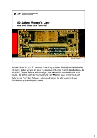
1. “Moore’s Law” ist nun 50 Jahre alt – der Chip auf dem Titelbild auch schon über
15 Jahre. Sollen wir uns an einer Hochschule mit einer Technik beschäftigen, die
so alt ist? Dieses Referat will aufzeigen, wie aktuell die Mikroelektronik auch
heute – 50 Jahre nach der Formulierung von “Moore’s Law” immer noch ist!
Referent ist Prof. Karl Schenk, Leiter des Instituts für Mikroelektronik der
Fachhochschule Nordwestschweiz.
1
2. Ich werde kurz “Moore’s Law” vorstellen, dann zeigen wo wir heute stehen und
was heute die Herausforderungen der Mikroelektronik sind. Ein Blick auf das IME
schliesst meine Präsentation ab.
2
4. “Moore’s Law” wurde von Gordon Moore, u.a. dem Mitbegründer von Intel, In der
Fachzeitschrift «Electronics» am 19. April 1965 formuliert. Moore’s Law ist kein
Gesetz, sondern eine Schlussfolgerung aus einer Beobachtung. Gordon Moore
postulierte, dass die Komplexität der Komponentenkosten sich um einen Faktor 2
pro Jahr erhöht hatte. Er gab seiner Überzeugung Ausdruck, dass diese
Steigerungsrate noch sicher 10 Jahre so weiter gehen würde und künftig ganze
komplexe Schaltungen auf einem einzigen Wafer möglich wären…
4
5. Die Grafik zeigt, aufgrund welcher Daten Gordon Moore seine Schlussfolgerung
zog: 1959 wurde erstmals ein «Chip», d.h. ein Element aus mehr als einem
einzigen Transistor auf dem selben Substrat produziert. 1965 konnten Chips mit
ca. 100 Transistoren hergestellt werden. Diese Kurve ergab extrapoliert bis 1075
ca. 65’000 erwartete Transistoren auf einem Chip…
5
6. Wo stehen wir heute: Die Halbleiter-Industrie erstellt alle zwei Jahre eine
«Technologie-Roadmap». Dabei wird der Status aufgenommen. Die
Herausforderungen in den verschiedenen Teildisziplinen werden analysiert, die
Lösungsansätze diskutiert und die Entwicklung auf die nächsten 10-20 Jahre
projiziert.
In der Vergangenheit war die ITRS jeweils ziemlich genau. Erstaunlich ist vor
allem, wie auch heute noch eine Entwicklung mit annähernd den gleichen
Steigerungsraten wie vor 50 Jahren gerechnet wird…
6
7. Diese Grafik zeigt die Entwicklung der Mikroprozessorchips seit dem ersten µP
(Intel 4004) im Jahre 1971 bis heute. Aufgetragen sind die wichtigsten µPs mit
ihrer Anzahl Transistoren. Dabei zeigt sich, dass in den 44 Jahren von 1971 bis
2015 eine Steigerung der Komplexität um einen Faktor 222 stattgefunden hat,
also eine Verdoppelung alle zwei Jahre.
7
8. Eine Grafik aus «Nature» verknüpft die Anzahl Transistoren (blau) mit der Gate
Länge, also der wichtigsten Technologie-Definition zur Strukturgrösse (rot). Zu
erkennen ist, dass die Strukturgrösse bis ins Jahr 2025 weiter von heute 10 nm
bis 7.4 nm sinken wird.
8
9. Die rasante Entwicklung gilt nicht nur für Prozessoren, sondern in ähnlichem
Masse auch für Speicherchips der verschiedenen Technologien: Auch hier ist in
der Grafik aus der ISSCC eine stete Erhöhung der Komplexität (der Anzahl
Speicherzellen pro Chip) zu erkennen – je nach Reife der Technologie mehr oder
weniger schnell.
9
10. Wie erreicht man auch heute noch diese Verdoppelung der Komplexität?
Einerseits werden Verfahren eingesetzt, welch emit «Strained Silicon» die
Gitterstruktur des Siliziums verändern, damit die Elektronen mobiler werden. Mit
high- κ Materialien, also Materialien mit höherer Dielektrizitätszahl als
Siliziumoxid, kann die Dicke des Gateoxids erhöht werden, was die Kapazität
erhöht und den Leckstrom senkt.
Materialien aus der sogenannten III-V-Gruppe wie Galliumarsenid,
Indiumphosphid etc. erhöhen ebenfalls die Geschwindigkeit der Bauteile.
Ausserdem werden neuartige Prinzipien wie Tunneling und Elektromagnetischer
Spin eingesetzt. Allerdings ist vorauszusehen, dass die horizontale Skalierung
von CMOS bald grundsätzliche Grenzen erreichen wird, weil die Grössenordnung
des Gitterabstands von Silizium erreicht wird.
Deshalb wird nach 50 Jahren der Weg in die dritte Dimension gesucht.
10
12. Als Zyklus bezeichnet die ITRS die Zeit für die Verdoppelung der Komplexität. Da
die Technologien bisher in 2D ausgeführt wurden, bedeutet «Verdoppelung der
Kapazität» immer eine Division der Strukturgrössen um die Wurzel von 2.
Prozessoren und ASICs folgten bisher einem Zyklus von 2 Jahren. Dieser wird
sich ab etwa 2017 auf 3 Jahre verlangsamen. Dynamische Speicher (DRAMs)
folgten bisher einem 3-Jahre-Zyklus und werden auf einen 4 Jahres Zyklus
zurückfallen. Damit werden die Prozessortechnologien jene der Speicher
einholen.
Mit der zunehmenden Verkleinerung der Strukturbreiten auf unter 10 nm nähern
sich diese immer mehr der Grösse des Silizium-Gitters: Hier beträgt der
Gitterabstand im Silizium-Kristall ca. 543 pm, somit sind bei einer Strukturgrösse
von 10 nm gerade noch etwa Kristalllagen vorhanden, bei einem FinFET (siehe
später) von 8 nm sogar nur 15 Kristallebenen. Es ist klar, dass dabei eine Grenze
erreicht wird und eine weitere Erhöhung der Dichte nur durch den Schritt in die
dritte Dimension erreichbar ist.
Es gibt Leute, welche das als «Moore’s Law 2.0» (oder sogar schon 3.0)
bezeichnen…
12
13. Die dritte Dimension kann auf verschiedenen Wegen gesucht werden.
Ein Weg ist, die Transistoren in die dritte Dimension wachsen zu lassen. Das
bedeutet, dass das Gate, das beim planaren MOS Transistor in der Ebene liegt,
neu aufgestellt wird. Es sieht dann aus wie eine Flosse (Fin) und wird von der
Gate-Elektrode umfasst. Dadurch werden die Wege sehr viel kürzer, die
Geschwindigkeit erhöht und auch die mögliche Dichte erhöht, weil nun auch
mehrere Gates pro Transistor möglich werden.
13
14. Die dritte Dimension wird aber auch erreicht, indem Chips aufeinander gestapelt
werden. Das wird schon seit einigen Jahren gemacht, dann aber, indem die
einzelnen Chips gegenüber dem Gehäuse und untereinander gebondet werden.
Heute werden die Chips hingegen durch den Wafer bzw. den Chip hindurch
miteinander verbunden, mit sogenannten «Through Silicon Via». Forschungen,
an denen auch ein Mitarbiter des IME beteiligt war, sind nun z.B. am IMEC im
Bereich des Test dieser TSV im Gang.
Stacking von Chips erlaubt nicht nur eine Erhöhung der Dichte, sondern auch die
Kombination von Chips in unterschiedlichen, auf die jeweiligen Anwendungen
optimierten Technologien, wie Prozessoren, Speicher, Analog-Funktionen und
Mikromechanik und deren schnelle Verbindung mit sehr vielen
Verbindungsstellen.
14
15. Neue Technologien wie «Spin-Wave-Materialien» erlauben nochmals eine
Erhöhung der Komplexität. Dabei werden elektromagnetische Spinwellen
erzeugt, gesteuert und übertragen.
15
16. Eine grosse Herausforderung bleibt der Energieverbrauch, und dabei auch das
Problem, wie die entstandene Wärme abgeführt werden kann. Gegen Ende des
letzten Jahrhunderts näherte sich die Energiedichte in den komplexesten
Prozessoren jener der Herdplatte, und befürchtet wurde bereits, dass diese
Energiedichte weiter ansteigen würde. Der Übergang zu neuen Technologien hat
aber dann zu einer Reduktion der Leckströme und des dynamischen
Energieverbauchs geführt, so dass die Leistungsdichte nun konstant geblieben
ist.
16
17. Generell ist die «Energie-Effizienz» gestiegen. Da moderne Rechner nicht immer
entweder gar nicht oder auf «Volllast» laufen, wird die Anzahl der Berechnungen
über ein Jahr mit dem Energieverbrauch während des Jahres mit allen Standby-,
Sleep- und Low-Power-Modi bewertet.
17
18. Bei den Standard-ICs wird auch heute noch Alumium für die Verdrahtung (Metal-
Layer) verwendet. Für High-Performance-Chips kommt seit vielen Jahren das
aufwändigere Kupfer zum Einsatz, das eine bessere Leitfähigkeit aufweist.
Bessere Materialien sind nicht in unmittelbarer Sicht, hingegen werden
Forschungsarbeiten mit Graphen, also einlagige Kohlenstoffschichten.
18
19. Eine weitere Herausforderung besteht ebenfalls schon seit vielen Jahren: Heute
wird immer noch UV-Licht mit 193 nm Wellenlänge zur Belichtung der
Chipstrukturen in der Produktion verwendet. Bei Strukturgrössen von 20 nm und
darunter ist die Wellenlänge somit ein Vielfaches der Struktur – somit muss die
Maske die optischen Streueffekte nachbilden. Extended UV mit 13 nm ist zwar
seit Langem bekannt, aber zu teuer, zuwenig lichtstark und noch nicht im breiten
Einsatz. Am PSI wird die SLS verwendet, um für Forschungszwecke EUV-
Lithographie zu machen – ein sehr aufwändiges Verfahren…
19
20. Schliesslich steigen mit der wachsenden Komplexität der ICs auch die
Anforderungen an den Design: Die Kosten wachsen nicht linear mit der
Komplexität, sondern exponentiell. Da auch die NRE-Kosten («Non-recurring
Engineering», Masken-Kosten etc.) exponentiell mit der Technologieentwicklung
ansteigen, werden FPGAs auch für komplexe integrierte Funktionen bei höheren
Stückzahlen wirtschaftlich, da die Programmierbarkeit nicht nur NRE-Kosten
spart, sondern auch das Designrisiko senkt. Vor Jahren wurde deshalb erwartet,
dass der ASIC-Markt für digitale ASICs massiv zurückgehen würde zugunsten
der FPGAs. Heute stellt man allerdings fest, dass sowohl der ASIC- als auch der
FPGA-Markt mehr oder weniger stabil sind. Trotzdem sind gerade im Schweizer
Markt die FPGAs absolut dominant – es gibt nur sehr wenige grosse Digital-
ASIC-Projekte.
20
21. Und wo steht bei alledem das Institut für Mikroelektronik (IME) der FHNW?
21
22. Im Bereich der rein digitalen ASICs sieht das IME praktisch nur FPGA-Projekte:
Diese können ihre Stärken bei schneller Signalverarbeitung mit hohen
Datenmengen, z.B. Echtzeit-Bildverarbeitung, ausspielen. Dabei bearbeitet das
IME grosse aufwändige Projekte wie den Echtzeit-Spektrumanalyse für die
Radiostronomie oder eine Bildverarbeitung für industrielle Drucksysteme und
wirkt damit an der Spitze der Technologie mit.
Während rein digitale «masken-produzierte» ASICs in der Schweiz nur eine
geringe Bedeutung haben, finden gemischt analog/digitale ASICs gerade in der
Medizintechnik oder in der Industriellen Mess- und Sensortechnik sehr viele
bestens geeignete Anwendungen. Aufgrund der Anforderungen und der in der
regel eher bescheidenen Stückzahlen genügen Technologien bis etwa 130 nm,
dafür kommen für die üblichen Anforderungen wie Low-Power und sehr
schwache Sensorsignale Schaltungstechniken wie Switched-Capacitor und
Wandlersystem als Sigma-Delta-Systeme zum Einsatz. Das IME beherrscht dazu
die Entwicklungs- und Simulationsmethodik und bearbeitet mehrere spannende
Industrieprojekte.
22