Downloaden Sie, um offline zu lesen


![W hen enter the BIOS Setup utility, follow the processes below for general use.
English
1. Load Optimized Defaults : Use control keys (↑↓) to highlight the Load Opti-
mized Defaults field and press <Enter> , a message as below appears:
Select [Ok] and press Enter to load the default settings for optimal system
performance.
2. Setup Date/ Time : Select the Standard CMOS Features and press <Enter> to
enter the Standard CMOS Features-menu. Adjust the Date, Time fields.
3. Save & Exit Setup : Use control keys (↑↓) to highlight the Save & Exit Setup
field and press <Enter> , a message as below appears:
Select [Ok] and press Enter to save the configurations and exit BIOS Setup utility.
Important
The configuration above are for general use only. If you need the detailed
settings of BIOS, please see the manual in English version on MSI website.
En-37](https://image.slidesharecdn.com/06-manualeclipseplus-091015160604-phpapp01/85/06-Manual-Eclipse-Plus-46-320.jpg)


![M S-7566 M ainboard
Intel Turbo Boost tech
This item will appear when you install a CPU include Intel Turbo Boost technology.
This item is used to enable/ disable Intel Turbo Boost technology. For further informa-
tion please refer to Intel's official website.
Turbo Boost Tech Config
This sub-menu will appear when you install a CPU include Intel Turbo Boost technology.
Press <Enter> to enter the sub-menu and the following screen appears.
Turbo Ratio Limit Program
This item is used to enable/ disable the turbo ratio limit program. Setting to [Enabled]
activates the following fields, and use the following fields to set each CPU core
ratio.
#-Core Ratio Limit
These items allow you to select the CPU core ratio.
TDC Limit Override
Setting to [Enabled] activates the TDC Limit value field, and use the TDC Limit
value field to set the CPU TDC value.
TDC Limit value (A)
This item allows you to select the CPU TDC value (ampere).
TDP Limit Override
Setting to [Enable] activates the TDP Limit value field, and use the TDP Limit
value field to set the CPU TDP value.
TDP Limit value (W)
This item allows you to select the CPU TDP value (watt).
OC Dial Function
This item allows you to enable/disable the OC Dial function. Setting to [Enabled]
activates the following fields, and use the following fields to set each OC Dial function.
En-40](https://image.slidesharecdn.com/06-manualeclipseplus-091015160604-phpapp01/85/06-Manual-Eclipse-Plus-49-320.jpg)
![OC Dial Step
English
This item is used to set value of each step when you rotate the OC dial knob.
OC Dial Reset
Select [Reset] if you need to reset the OC Dial Value.
OC Dial Value
This item indicates the overclocking value by OC dial function. W hen you rotate the
OC dial knob, this value will change.
OC Dial Adjusted Base Clock (MHz)
It shows the adjusted base clock by OC Dial function (Base Clock +OC Dial Value).
Read-only.
Adjusted Core Frequency (M Hz)
It shows the adjusted CPU frequency (Base clock x Ratio). Read-only.
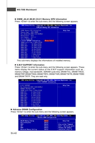
QPI Configuration
Press <Enter> to enter the sub-menu and the following screen appears.
QPI Links Speed
This item allows you to select the QPI links speed type.
QPI Frequency
This item allows you to select the QPI frequency.
M emory -Z
Press <Enter> to enter the sub-menu and the following screen appears.
En-41](https://image.slidesharecdn.com/06-manualeclipseplus-091015160604-phpapp01/85/06-Manual-Eclipse-Plus-50-320.jpg)
![1N/2N M emory Timing
English
This item controls the SDRAM command rate. Select [1N] makes SDRAM signal
controller to run at 1N (N=clock cycles) rate. Selecting [2N] makes SDRAM signal
controller run at 2N rate.
CAS# Latency (CL)
This controls the CAS latency, which determines the timing delay (in clock cycles)
before SDRAM starts a read command after receiving it.
tRCD
W hen DRAM is refreshed, both rows and columns are addressed separately.
This setup item allows you to determine the timing of the transition from RAS
(row address strobe) to CAS (column address strobe). The less the clock
cycles, the faster the DRAM performance.
tRP
This setting controls the number of cycles for Row Address Strobe (RAS) to be
allowed to precharge. If insufficient time is allowed for the RAS to accumulate its
charge before DRAM refresh, refresh may be incomplete and DRAM may fail to
retain data. This item applies only when synchronous DRAM is installed in the
system.
tRAS
This setting determines the time RAS takes to read from and write to memory
cell.
Advanced M emory Setting
Setting to [Auto] enables the advance memory timing automatically to be deter-
mined by BIOS. Setting to [Manual] allows you to set advanced memory timings.
Extreme M emory Profile
This item is used to enable/disable the Intel Extreme Memory Profile (XMP). For further
information please refer to Intel's official website.
M emory Ratio
This item allows you to set the memory multiplier.
Adjusted DRAM Frequency (MHz)
It shows the adjusted DDR Memory frequency. Read-only.
ClockGen Tuner
Press <Enter> to enter the sub-menu and the following screen appears.
En-43](https://image.slidesharecdn.com/06-manualeclipseplus-091015160604-phpapp01/85/06-Manual-Eclipse-Plus-52-320.jpg)
![M S-7566 M ainboard
CPU / PCI Express Amplitude Control
These items are used to select the CPU/ PCI Express clock amplitude.
CPU CLK Skew/ IOH CLK Skew
These items are used to select the CPU/ IOH chipset clock skew. They can help
CPU to reach the higher overclocking performace.
Adjust PCI Frequency (MHz)
This field allows you to select the PCI frequency (in MHz).
Adjust PCI-E Frequency (MHz)
This field allows you to select the PCIE frequency (in MHz).
Auto Disable DRAM /PCI Frequency
W hen set to [Enabled], the system will remove (turn off) clocks from empty DIMM and
PCI slots to minimize the electromagnetic interference (EMI).
CPU Load Line Calibration
This item allows you to enable/disable CPU Load Line Calibration.
CPU Voltage (V)/ CPU Vcore/ QPI Voltage (V))/ CPU PLL Voltage (V)/ DRAM
Voltage (V)/ DDR_VREF_CA_A (V)/ DDR_VREF_CA_B (V)/ DDR_VREF_CA_C (V)/
DDR_VREF_DQ_A (V)/DDR_VREF_DQ_B (V), DDR_VREF_DQ_C (V)/ IOH Voltage
(V)/ IOH PCIE Voltage (V)/ ICH Voltage (V)/ nForce 200 Voltage (V)
These items are used to asjust the voltage of CPU, Memory, QPI and chipset.
For CPU Voltage:
The value here is the offset for you to adjust/add based on the current CPU voltage.
Please read the real-time CPU voltage in “CPU Vcore”. Please note the based CPU
Voltage will vary depending on the different CPU you install.
For QPI Voltage:
The value here is the offset for you to adjust/add based on the current QPI voltage.
The default based QPI Voltage is from 1.1V to 1.22V, and it will vary depending on the
different CPU you install. You can read the QPI voltage in GreenPower Center.
For DRAM Voltage:
According to the Inte CPU spec, DRAM Voltage setting 1.65V may damage the CPU
permanently. It is strongly recommended that you install the DRAM with the voltage
setting below 1.65V. You can read the DRAM voltage in GreenPower Center.
Spread Spectrum
W hen the motherboard’s clock generator pulses, the extreme values (spikes) of the
pulses create EMI (Electromagnetic Interference). The Spread Spectrum function
reduces the EMI generated by modulating the pulses so that the spikes of the pulses
are reduced to flatter curves. If you do not have any EMI problem, leave the setting at
Disabled for optimal system stability and performance. But if you are plagued by EMI,
set to Enabled for EMI reduction. Remember to disable Spread Spectrum if you are
overclocking because even a slight jitter can introduce a temporary boost in clock
speed which may just cause your overclocked processor to lock up.
En-44](https://image.slidesharecdn.com/06-manualeclipseplus-091015160604-phpapp01/85/06-Manual-Eclipse-Plus-53-320.jpg)
![English
Important
1. If you do not have any EMI problem, leave the setting at [Disabled] for
optimal system stability and performance. But if you are plagued by EMI,
select the value of Spread Spectrum for EMI reduction.
2. The greater the Spread Spectrum value is, the greater the EMI is reduced,
and the system will become less stable. For the most suitable Spread
Spectrum value, please consult your local EMI regulation.
3. Remember to disable Spread Spectrum if you are overclocking because
even a slight jitter can introduce a temporary boost in clock speed which
may just cause your overclocked processor to lock up.
En-45](https://image.slidesharecdn.com/06-manualeclipseplus-091015160604-phpapp01/85/06-Manual-Eclipse-Plus-54-320.jpg)


![Wenn Sie das BIOS Dienstprogramm öffnen, folgen Sie den untenstehenden
Anweis ungen.
1. Laden der optimalen Voreinstellung : Verwenden Sie die Steuerschlüssel (
↑↓ ), um dem Laden der optimalen Voreinstellung zu wählen und drücken Sie
auf <Eingabe>. Dann erscheint die folgende Meldung:
Deutsch
Drücken Sie auf [OK] und <Enter>, um die im Werk eingestellten Standardwerte
für eine optimale Systemleistung zu laden.
2. Die Datum/Zeit Einstellung : W ählen Sie die “Standard-CMOS Features” vor
und drücken Sie <Eingabe> um das Standard-CMOS Features-Menü zu wählen.
Passen Sie nun die Felder “Datum” und “Zeit” an.
3. Abspeichern u. Beenden der Einstellung: Verwenden Sie die Steuerschlüssel
(↑↓ ), um dem Abspeichern u. Beenden der Einstellungen zu wählen und
drücken Sie auf <Eingabe>. Es erscheint folgende Meldung:
Drücken Sie auf [OK] und <Enter>, um die (neuen) Einstellungen zu speichern und
das BIOS Setup zu verlassen.
Wichtig
Die Konfiguration oben dienen nur generellen Zwecken. Wenn Sie detaillierte
BIOS- Einstellungen benötigen, dann s ehen Sie bitte das Handbuch in
Englischer Sprache auf der MSI Website ein.
De-37](https://image.slidesharecdn.com/06-manualeclipseplus-091015160604-phpapp01/85/06-Manual-Eclipse-Plus-92-320.jpg)


![M S-7566 M ainboard
Intel Turbo Boost tech
Das Untermenü erscheint, wenn Sie eine CPU anbringen, die die Intel Turbo Boost
Technologie aufnehmt. Und hier können Sie die Intel Turbo Boost Technologie aktiviert/
deaktiviert. Für weitere Informationen beziehen Sie in offizielle Website des Intel.
Turbo Boost Tech Config
Das Untermenü erscheint, wenn Sie eine CPU anbringen, die die Intel Turbo Boost
Technologie aufnehmtDrücken Sie die Eingabetaste <Enter>, um das folgende
Untermenü aufzurufen.
Turbo Ratio Limit Program
Hier können Sie dasTurbo Ratio Limit Program aktivieren/ deaktivieren. Lautet die
Einstellung auf [Enabled] (eingeschaltet), aktiviert die folgenden Option, um jede
CPU Core Ratio einzustellen.
#-Core Ratio Limit
Hier können Sie das CPU Core Ratio auswählen.
TDC Limit Override
Die Einstellungen [Enable] (eingeschaltet), aktiviert den TDC Limit Wert und
verwenden diesen TDC Limit Wert , um den CPU TDC Value einzustellen.
TDC Limit value (A)
Hier können Sie den CPU TDC Wert (ampere) auswählen.
TDP Limit Override
Die Einstellungen [Enable] (eingeschaltet), aktiviert den TDP Limit Wert und
verwenden diesen TDP Limit Wert , um den CPU TDP Value einzustellen.
TDP Limit value (W)
Hier können Sie den CPU TDP Wert (watt) auswählen.
OC Dial Function
Hier können Sie die OC Dial-Funktion aktivieren/ deaktivieren . Lautet die Einstellung
De-40](https://image.slidesharecdn.com/06-manualeclipseplus-091015160604-phpapp01/85/06-Manual-Eclipse-Plus-95-320.jpg)
![auf [Enabled] (eingeschaltet), aktiviert die folgenden Option, um jede OC Dial-Funktion
einzustellen.
Deutsch
OC Dial Step
Hier können Sie den Wert jedes Schrittes einstellen, wenn Sie den OC Dialknopf
drehen.
OC Dial Reset
W ählen Sie [Reset] aus, wenn Sie den OC Dial Wert zurückstellen müssen.
OC Dial Value
Hier zeigt den Übertaktungwert durch OC Dial Funktion an. Wenn Sie den OC Dialknopf,
ändert der Wert.
OC Dial Adjusted Base Clock (MHz)
Zeigt den eingestellten FSB Takt durch OC Dial Funktion (FSB Clock +OC Dial Value).
Nur Anzeige.
Adjusted Core Frequency (M Hz)
Gibt der verstellt Frequenz des CPU (Grundtakt x Ratio). Nur Anzeige.
QPI Configuration
Drücken Sie die Eingabetaste <Enter>, um das folgende Untermenü aufzurufen.
QPI Links Speed
Hier können Sie die QPI Link Geschwindigkeittyp auswählen.
QPI Frequency
Hier können Sie die QPI Frequenz auswählen.
M emory -Z
Drücken Sie die Eingabetaste <Enter>, um das folgende Untermenü aufzurufen.
De-41](https://image.slidesharecdn.com/06-manualeclipseplus-091015160604-phpapp01/85/06-Manual-Eclipse-Plus-96-320.jpg)

![1N/2N M emory Timing
Können Sie hier die DRAM Timing angeben. Legt die SDRAM Kommandorate fest.
Die Einstellung 1N lässt den SDRAM Signal Kontroller mit einem 1N ((Taktzyklus)
laufen. Bei 2N läuft er mit zwei Zyklen. 1N ist schneller als 2N.
CAS# Latency (CL)
Hier wird die Verzögerung im Timing (in Taktzyklen) eingestellt, bevor das SDRAM
Deutsch
einen Lesebefehl nach dessen Erhalt auszuführen beginnt.
tRCD
Wenn DRAM erneuert wird, werden Reihen und Spalten separat adressiert. Dies
gestattet es, die Anzahl der Zyklen und der Verzogerung im Timing einzustellen,
die zwischen den CAS und RAS Abtastsignalen liegen, die verwendet werden,
wenn der DRAM beschrieben, ausgelesen oder aufgefrischt wird. Eine hohe
G es c h wi n d i g k ei t f ü h r t z u h öh er e r L ei s t u n g , w äh r en d l an g s am er e
Geschwindigkeiten einen stabileren Betrieb bieten.
tRP
Legt die Anzahl der Taktzyklen fest, die das Reihenadressierungssignal (Row
Address Strobe - RAS) für eine Vorladung bekommt. W ird dem RAS bis zur
Auffrischung des DRAM nicht genug Zeit zum Aufbau seiner Ladung gegeben,
kann der Refresh unvollständig ausfallen und das DRAM Daten verlieren. Dieser
Menüpunkt ist nur relevant, wenn synchroner DRAM verwendet wird.
tRAS
Stellt die Zeit der RAS Lese- und Schreibzugriffe ein.
Advanced M emory Setting
Die Einstellung [Auto] ermöglicht dem vorgerückten Speicher-Timing, die von
BIOS automatisch festgestellt wird. Lautet die Einstellung [Manual], können Sie
hier die vorgerückte Speicher-Timing angeben.
Extreme M emory Profile
Hier können Sie das Extreme-Memory-Profile (X.M.P.) aktiviert/ deaktiviert. Für weitere
Informationen beziehen Sie in offizielle Website des Intel.
M emory Ratio
Hier können Sie die Speicher-Multiplikator.
Adjusted DRAM Frequency (MHz)
Gibt den geänderten Frequenz-Wert des DDR Speicher an. Nur Anzeige.
ClockGen Tuner
Drücken Sie die Eingabetaste <Enter>, um das folgende Untermenü aufzurufen.
De-43](https://image.slidesharecdn.com/06-manualeclipseplus-091015160604-phpapp01/85/06-Manual-Eclipse-Plus-98-320.jpg)
![M S-7566 M ainboard
CPU / PCI Express Amplitude Control
Gestattet die Wahl der CPU-Takt oder PCI-E Takt.
CPU CLK Skew/ IOH CLK Skew
Gestattet die W ahl der CPU/ IOH Chipsatztakt,durch Einstellung eines höheren
CPU Taktes.
Adjust PCI Frequency (MHz)
Gestattet die W ahl der PCI Frequenz (in MHz).
Adjust PCI-E Frequency (MHz)
Gestattet die Wahl der PCI-E Frequenz (in MHz).
Auto Disable DRAM /PCI Frequency
Lautet die Einstellung auf [Enabled] (eingeschaltet), deaktiviert das System die Taktung
leerer PCI Sockel, um die Elektromagnetische Störstrahlung (EMI) zu minimieren.
CPU Load Line Calibration
Hier können Sie die CPU Ladelinie Kalibrierung aktivieren/deaktivieren.
CPU Voltage (V)/ CPU Vcore/ QPI Voltage (V))/ CPU PLL Voltage (V)/ DRAM
Voltage (V)/ DDR_VREF_CA_A (V)/ DDR_VREF_CA_B (V)/ DDR_VREF_CA_C (V)/
DDR_VREF_DQ_A (V)/DDR_VREF_DQ_B (V), DDR_VREF_DQ_C (V)/ IOH Voltage
(V)/ IOH PCIE Voltage (V)/ ICH Voltage (V)/ nForce 200 Voltage (V)
Diese Option bietet bietet die Moglichkeit, die Spannung der CPU, des Speichers und
des QPI sowie des Chipsatz anzupassen.
For CPU Voltage:
Dieser Eintrag ermoglicht innerhalb eines Bereiches die CPU Spannung zu ändern /
anzupassen. Lesen Sie dazu die Standard CPU-Spannung “CPU Vcore” auf der “H/W
Monitor” BIOS Seite nach. Bitte beachten Sie, dass die CPU Spannung je nach
eingesetzter CPU variieren kann.
For QPI Voltage:
Dieser Eintrag ermöglicht innerhalb eines Bereiches die QPI Spannung zu ändern /
anzupassen. Die Standardspannung liegt zwischen 1.1V und 1.22V und varriiert, je
nach eingesetzter CPU. Im Green Power Center haben Sie die Möglichkeit, die QPI
Spannung zu erhalten.
Für DRAM Spannung:
Laut Intel Spezifikationen kann eine DRAM Spannung von 1,65V und mehr die CPU
beschädigen. Bitte achten Sie beim Einstellen des Wertes darauf, unter dem Wert der
Intel Vorgaben zu bleiben. Im Green Power Center haben Sie die Möglichkeit, die
DRAM Spannung zu erhalten.
Spread Spectrum
Pulsiert der Taktgenerator des Motherboards, erzeugen die Extremwerte (Spitzen)
der Pulse EMI (Elektromagnetische Interferenzen). Die Spread Spectrum Funktion
reduziert die erzeugten EMI, indem die Pulse so moduliert werden, das die Pulsspitzen
zu flacheren Kurven reduziert werden.
De-44](https://image.slidesharecdn.com/06-manualeclipseplus-091015160604-phpapp01/85/06-Manual-Eclipse-Plus-99-320.jpg)
![Wichtig
1. Sollten Sie keine Probleme mit Interferenzen haben, belassen Sie es bei
d e r E in s t e llu n g [ D is ab le d ] ( a u s g e s c h a l t e t ) , u m b e s t m ö g lic h e
Deutsch
Systemstabilität und -leistung zu gewährleisten. Stellt für sie EMI ein Prob-
lem dar, wählen Sie die gewünschte Bandbreite zur Reduktion der EMI.
2. Je größer Spread Spectrum Wert ist, desto größer nimmt der EMI ab, und
das System wird weniger stabil. Bitte befragen Sie Ihren lokalen EMI
Regelung zum meist passend Spread Spectrum Wert.
3. Denken Sie daran Spread Spectrum zu deaktivieren, wenn Sie übertakten,
da sogar eine leichte Schwankung eine vorübergehende Taktsteigerung
erzeugen k ann, die gerade ausreic hen mag, um Ihren übertakteten
Prozessor zum einfrieren zu bringen.
De-45](https://image.slidesharecdn.com/06-manualeclipseplus-091015160604-phpapp01/85/06-Manual-Eclipse-Plus-100-320.jpg)


![Quand vous entrez dans l’unité de réglages BIOS, suivez les procédures suivantes
pour l’utilisation générale.
1. Load Optimized Defaults (chargement des réglages par défaut optimisés)
: Utilisez les touches de contrôle (↑↓) afin de surligner le domaine Load Opti-
mized Defaults et appuyez sur <Enter> , le message suivant apparaîtra :
Choisir [Ok] et appuyer sur Enter chargera les valeurs défauts de BIOS pour un
système minimal plus stable.
Français
2. Setup Date/ Time (Réglage de l’heure et de la date) : Choisissez Standard
CM OS Features et appuyez sur <Enter> afin d’entrer dans le menu Standard
CMOS Features. Ajustez la date et l’heure.
3. Save & Exit Setup (Sauvegarder et quitter les réglages) : Utilisez les touches
de contrôle (↑↓) afin de surligner le domaine de Save & Exit Setup et appuyez
sur <Enter> , le message suivant apparaîtra :
Choisir [Ok] et appuyer sur Enter afin de sauvegarder les configurations et l’unité
de réglages de quitter BIOS.
Important
Les configurations précédantes ne sont que pour l’utilisation générale. Si
vous avez besoin de réglages détaillés du BIOS, veuillez vous référer au
manuel de l’édition anglaise sur la page d’internet de MSI.
Fr-37](https://image.slidesharecdn.com/06-manualeclipseplus-091015160604-phpapp01/85/06-Manual-Eclipse-Plus-138-320.jpg)

![Carte mère M S-7566
Intel Turbo Boost tech
Cet article apparaît quand vous installez un CPU avec la technologie Intel Turbo Boost
y compris. Cet article sert à activer/ désactiver la technologie Intel Turbo Boost. Pour
plus d’informations veuillez vous référer au site officiel d’Intel.
Turbo Boost Tech Config
Ce sous-menu apparaît quand vous installez un CPU avec la technologie Intel Turbo
Boost y compris. Appuyez sur <Enter> pour entrer dans le sous-menu et il apparaît
l’écran suivant.
Turbo Ratio Limit Program
Cet article sert à activer/ désactiver la programme turbo ratio limit. La mise en
[Enabled] active les domaines suivants, et les utilise pour régler chaque CPU
core ratio.
#-Core Ratio Limit
Ces articles vous permettent de choisir le CPU core ratio.
TDC Limit Override
La mise en [Enabled] active le domaine TDC Limit value, et utilise le domaine
TDC Limit value pour régler la valeur CPU TDC.
TDC Limit value (A)
Cet article vous permet de choisir la valeur CPU TDC (ampere).
TDP Limit Override
La mise en [Enable] active le domaine TDP Limit value, et utilise le domaine TDP
Limit value pour régler la valeur CPU TDP.
TDP Limit value (W)
Cet article vous permet de choisir la valeur CPU TDP (watt).
OC Dial Function
Cet article vous permet d’activer/ désactiver la fonction OC Dial. La mise en [Enabled]
active les domaines suivants, et les utilise pour régler chaque fonction OC Dial.
Fr-40](https://image.slidesharecdn.com/06-manualeclipseplus-091015160604-phpapp01/85/06-Manual-Eclipse-Plus-141-320.jpg)
![OC Dial Step
Cet article vous sert à régler la valeur de chaque étape quand vous tournez la
poignée OC dial.
OC Dial Reset
Choisissez [Reset] si vous voulez remettre la valeur OC Dial.
OC Dial Value
Cet article indique la valeur d’overclocking par la fonction OC dial. Quand vous tournez
la poignée OC dial, cette valeur change.
OC Dial Adjusted Base Clock (MHz)
Il montre l’horloge de base ajustée par la fonction OC Dial (Horloge de base + Valeur
Français
OC Dial). Lecture uniquement.
Adjusted Core Frequency (M Hz)
Il montre la fréquence ajustée du CPU (Horloge de base x Ratio). Lecture uniquement.
QPI Configuration
Appuyez sur <Enter> pour entrer dans le sous-menu et il apparaît l’écran suivant.
QPI Links Speed
Cet article vous permet de choisir le type de vitesse de lien QPI.
QPI Frequency
Cet article vous permet de choisir la fréquence QPI.
M emory -Z
Appuyez sur <Enter> pour entrer dans le sous-menu et il apparaît l’écran suivant.
Fr-41](https://image.slidesharecdn.com/06-manualeclipseplus-091015160604-phpapp01/85/06-Manual-Eclipse-Plus-142-320.jpg)

![1N/2N M emory Timing
Cet article contrôle le taux d’ordre du SDRAM. La sélection en [1N] fait fonctionner
en taux de 1N (N=cycles d’horloge) au contrôleur du signaux du SDRAM. La
sélection en [2N] fait fonctionner en taux de 2N au contrôleur du signaux du
SDRAM.
CAS# Latency (CL)
Cela contrôle le latence CAS, qui détermine le retard de timing (dans les cycles
d’horloge) avant que le SDRAM commence un ordre de lecture après l’avoir
reçu.
tRCD
Quand le DRAM est rafraîchi, les rangs et les colonnes sont tous adressés
séparément. Cet article vous permet de déterminer le timing de la transition de
RAS (row address strobe) à CAS (column address strobe). Le moins fonctionne
Français
l’horloge, le plus vite est la performance de DRAM.
tRP
Cet article contrôle le numéro de cycles pour que le Row Address Strobe (RAS)
soit permit de précharger. S’il n’y a pas assez de temps pour que le RAS accumule
son charge avant le refraîchissement de DRAM, le refraîchissement peut être
incomplet et le DRAM peut échouer à retenir les données.Cet article applique
seulement quand le DRAM synchrone est installé dans le système.
tRAS
Cet article détermine le temps que le RAS prend pour lire ou écrire sur une cellule
de mémoire.
Advanced M emory Setting
La mise en [Auto] rend le timing de mémoire avancée automatiquement déterminé
par BIOS. La mise en [Manual] vous permet de régler les timings de mémoire
avancée.
Extreme M emory Profile
Cet article sert à activer/désactiver le Intel Extreme Memory Profile (XMP). Pour plus
d’informations, veuillez vous référer au site officiel d’Intel.
M emory Ratio
Cet article vous permet de régler le multiplicateur de la mémoire.
Adjusted DRAM Frequency (MHz)
Il montre la fréquence de la mémoire DDR ajustée. Lecture uniquement.
ClockGen Tuner
Appuyez sur <Enter> pour entrer dans le sous-menu et il apparaîtra l’écran suivant.
Fr-43](https://image.slidesharecdn.com/06-manualeclipseplus-091015160604-phpapp01/85/06-Manual-Eclipse-Plus-144-320.jpg)

![Spread Spectrum
Lorsque le générateur d’horloge de la carte mère fonctionne, les valeurs extrêmes
(spikes ) créent des interférenc es élec tromagnétiques (EMI-Elec tromagnetic
Interference). La fonction Spread Spectrum réduit ces interférences en réglant les
impultions. Si vous n’avez pas de problème d’EMI ceci vous permet d’avoir une stabilité
du système et des performances optimales. Dans le cas contraire, choisissez En-
abled pour réduire les interférences. N’oubliez pas de désactiver cette fonction si
vous voulez faire de l’overclocking, parce que la moindre modification peut entraîner
une accélération temporaire d’horloge et ainsi votre processeur overclocké se
verrouillera.
Français
Important
1. Si vous n’avez pas de problème d’EMI, laissez l’option sur [Disabled]
ceci vous permet d’avoir une stabilité du système et des performances
optimales. Dans le cas contaire, choisissez Spread Spectrum pour réduire
les EMI.
2. Plus la valeur Spread Spectrum est importante, plus les EMI sont réduites,
et le système devient moins stable. Pour la valeur Spread Spectrum la
plus convenable, veuillez consulter le règlement EMI local.
3. N’oubliez pas de désactiver la fonction Spread Spectrum si vous êtes en
train d’overclocker parce que même un battement léger peut causer un
accroissement temporaire de la vitesse de l’horloge qui verrouillera votre
processeur overclcké.
Fr-45](https://image.slidesharecdn.com/06-manualeclipseplus-091015160604-phpapp01/85/06-Manual-Eclipse-Plus-146-320.jpg)


![В общем случае, находясь в режиме настройки BIOS, рекомендуется выполнить
следующие действия.
1. Load Optimized Defaults : Клавишами управления (↑↓) выберите пункт
Load Optimiz e d Defaults и нажми те <Enter>, появитс я с ледующее
сообщение:
Нажмите [Ok], чтобы загрузить настройки по умолчанию для оптимальной
производительности системы.
2. Setup Date/ Time : Выберьте Standard CMOS Features и нажмите <Enter>
для входа в меню. Установите дату и время в соответствующих полях.
Русский
3. Save & Exit Setup : Клавишами управления (↑↓) выберьте пункт Save &
Exit Setup и нажмите <Enter>, появится следующее сообщение:
Нажмите [Ok], чтобы сохранить конфигурацию и выйти из BIOS Setup.
Внимание
Приведенная выше конфигурация подходит для общего применения.
Если же вам требуются более тонкие настройки BIOS, обратитесь к
английской версии руководства на веб-сайте MSI.
Ru-37](https://image.slidesharecdn.com/06-manualeclipseplus-091015160604-phpapp01/85/06-Manual-Eclipse-Plus-184-320.jpg)


![MS-7566 Системная плата
Base Clock (М Гц)
Этот пункт позволяет установить CPU Base clock (в МГц).
Intel Turbo Boost tech
Этот п укнт появл яетс я, ког да вы ус тан овили CPU , поддержи вающий
технологию Intel T urbo Boos t. Этот пункт ис поль зуетс я для включения/
выключения технологии Intel Turbo Boost. Более подробную информацию можно
получить на оффициальном вебсайте Intel.
Turbo Boost Tech Config
Это подменю появляется при установке CPU, поддерживающего технологию
IIntel T urbo Boost. Нажмите <Enter> для входа в подменю и появляется
нижеследующий экранs.
Turbo Ratio Limit Program
Этот пункт используется для включения/ выключения программы turbo
ratio limit. Установка в [Enabled] активизирует следующие пункты, здесь вы
можете установить множитель CPU для каждого ядра.
#-Core Ratio Limit
Эти пункты позволяют выбрать множитель ядра CPU.
TDC Limit Override
Установка в [Enabled] активизирует пункт TDC Limit value, и позволяет
установить значение TDC CPU.
TDC Limit value (A)
Этот пункт позволяет выбрать CPU TDC value (амперы).
TDP Limit Override
Установка в [Enable] активизирует пункт TDP Limit value, и позволяет
установить значение TDP CPU.
TDP Limit value (W)
Этот пункт позволяет выбрать CPU TDP value (ватты).
OC Dial Function
Этот пункт позволяет включить/выключить функцию OC Dial. Установка в [En-
abled] активизирует соответствующие пункты, используйте их для настройки
данной функции.
Ru-40](https://image.slidesharecdn.com/06-manualeclipseplus-091015160604-phpapp01/85/06-Manual-Eclipse-Plus-187-320.jpg)
![OC Dial Step
Этот пункт ис п оль зуетс я для ус тановки шаг а изменен ия час тот ы при
использовании регулятора OC Dial.
OC Dial Reset
Выберите [Reset], если вам нужно сбросить значение OC Dial Value.
OC Dial Value
Этот пункт показывает величину разгона через функцию OC Dial. Когда вы
регулируйте OC Dial, это значение будет меняться.
OC Dial Adjusted Base Clock (МГц)
Этот пункт показывает base clock, установленной с помощью OC Dial (Base
Clock +OC Dial Value). Только для чтения.
Adjusted Core Frequency (М Гц)
Русский
Этот пункт показывает текущее значение тактовой частоты CPU (Base clock x
Ratio). Только для чтения.
QPI Configuration
Нажмите <Enter> для входа в подменю и появляется нижеследующий экранs.
QPI Links Speed
Этот пункт позволяет выбрать тип скорости передачи QPI.
QPI Frequency
Этот пункт позволяет установить тактовую частоту QPI.
M emory -Z
Нажмите <Enter> для входа в подменю и появляется нижеследующий экранs.
Ru-41](https://image.slidesharecdn.com/06-manualeclipseplus-091015160604-phpapp01/85/06-Manual-Eclipse-Plus-188-320.jpg)

![1N/2N M emory Timing
Этот пункт определяет скорость выдачи команд SDRAM. Выбор [1N] переводит
сигнальный котроллер SDRAM в режим работы 1N (N=clock cycles). Выбор
[2N] переводит сигнальный котроллер SDRAM в режим работы 2N.
CAS# Latency (CL)
Этот пункт контролирует время задержки CAS, которое определяет период
(в тактах генератора) между получением SDRAM команды чтения и
началом ее выполнения.
tRCD
При регенерации заряда DRAM, строки и столбцы адресуются раздельно.
Этот пункт позволяет вам определить время перехода от RAS (строб
адреса строки) к CAS (строб адреса столбца). Чем меньше тактов, тем
быстрее работа DRAM.
tRP
Этот пункт контролирует количес тво тактов, предос тавляемых для
предзаряда Row Address Strobe (RAS). Если выделяется недостаточное время
Русский
для того, чтобы RAS набрал необходимый заряд, регенерация DRAM может
оказаться неполной и привести к потере данных. Этот пункт применим, только
когда в системе установлена синхронная DRAM.
tRAS
Эта установка определяет время, которое RAS затрачивает на чтение и
запись в ячейку памяти.
Advanced M emory Setting
Установка в [Auto] даёт возможнос ть BIOS автоматически определять
т а й м и н г и п ам я т и . Ус т а н ов к а в [ M an u al ] п о з в ол я ет ус т а н ов и т ь
дополнительные тайминги памяти.
Extreme M emory Profile
Этот пункт позволяет включить/выключить Intel Extreme Memory Profile (XMP).
За дополнительной информацией обращайтесь на официальный вебсайт Intel.
M emory Ratio
Этот пункт позволяет установить множитель памяти.
Adjusted DRAM Frequency (МГц)
Этот пункт показывает текущую частоту памяти DDR. Только для чтения.
ClockGen Tuner
Нажмите <Enter> для входа в подменю и появляется нижеследующий экранs.
Ru-43](https://image.slidesharecdn.com/06-manualeclipseplus-091015160604-phpapp01/85/06-Manual-Eclipse-Plus-190-320.jpg)
![MS-7566 Системная плата
CPU / PCI Express Amplitude Control
Эти пункты используются для выбора амплитуды тактового сигнала CPU/
PCI Express.
CPU CLK Skew/ IOH CLK Skew
Эти пункты используются для выбора задержек тактового сигнала для
CPU/ IOH, это может улучшить результаты разгона CPU.
Adjust PCI Frequency (М Гц)
Этот пункт позволяет установить частоту PCI (в МГц).
Adjust PCI-E Frequency (МГц)
Этот пункт позволяет установить частоту PCIE (в МГц).
Auto Disable DRAM /PCI Frequency
При установке значения [Enabled], система отключит неиспользуемые разъемы
памяти и PCI, что приведёт к снижению уровня электромагнитных помех (EMI).
CPU Load Line Calibration
Этот пункт позволяет включить/выключить CPU Load Line Calibration.
CPU Voltage (V)/ CPU Vcore/ QPI Voltage (V))/ CPU PLL Voltage (V)/ DRAM
Voltage (V)/ DDR_VREF_CA_A (V)/ DDR_VREF_CA_B (V)/ DDR_VREF_CA_C (V)/
DDR_VREF_DQ_A (V)/DDR_VREF_DQ_B (V), DDR_VREF_DQ_C (V)/ IOH Voltage
(V)/ IOH PCIE Voltage (V)/ ICH Voltage (V)/ nForce 200 Voltage (V)
Эти пункты позволяют регулировать напряжение CPU, памяти, QPI и чипсета.
For CPU Voltage:
Эт от п ун кт и с п оль зует с я д ля ус тановк и с м ещ ен ия напр яжен ия C PU
относительно текущего значения. Получить информацию о напряжении CPU
можно в пункте “CPU Vcore”. Обратите внимание на то, что номинальное
напряжение CPU варьирует в зависимости от процессора, установленного
вами.
For QPI Voltage:
Э тот п унк т и с п оль з ует с я дл я ус т анов ки с м ещен ия напр я жен ия Q P I
относительно текущего значения. Напряжение QPI по умолчанию варьирует
от 1.1V до 1.22V, в зависимости от CPU, ус тановленного вами. Значение
напряжения QPI можно увидеть в GreenPower Center.
For DRAM Voltage:
В соответствии со спецификацией Intel CPU, установка напряжения DRAM в 1.
65 V м ожет ис пор тит ь C PU. Нас тоя тел ь но рек омендуетс я ус тан ови ть
напряжение DRAM ниже 1.65V. Значение напряжения DRAM можно увидеть в
GreenPower Center.
Ru-44](https://image.slidesharecdn.com/06-manualeclipseplus-091015160604-phpapp01/85/06-Manual-Eclipse-Plus-191-320.jpg)
![Spread Spectrum
Так как тактовый генератор сис темной платы импульс ный, то его работа
вызывает электромагнитные помехи - EMI (Electromagnetic Interference). Функция
Spread Spectrum снижает эти помехи, генерируя сглаженные импульсы. Если
у вас нет проблем с помехами, оставьте значение [Disabled] (запрещено) для
лучшей стабильности и производительности. Однако, если у вас возникают
электромагнитные помехи, разрешите использование этой функции, установив
[Enabled](разрешено). Не забудьте запретить использование функции Spread
Spectrum, если вы “разгоняете” системную плату. Это необходимо, так как
даже небольшой дребезг сигналов тактового генератора может привести к
отказу “разогнанного” процессора.
Внимание
Русский
1. Если у вас нет проблем с помехами, оставьте значение [Disabled]
(запрещено) для лучшей стабильности и производительности.
Однако, если у вас возникают электромагнитные помехи, выберите
Spread Spectrum для их уменьшения.
2. Чем больше значение Spread Spectrum, тем ниже будет уровень
электромагнитных помех, но система станет менее стабильной. Для
выбора подходящего значения Spread Spectrum, сверьтесь со значениями
уровней электромагнитных помех, установленных законодательством.
3. Не забудьте запретить использование функции Spread Spectrum,
если вы ”разгоняете” системную плату. Это необходимо, так как
даже небольшой дребезг сигналов тактового генератора может
привести к отказу ”разогнанного” процессора.
Ru-45](https://image.slidesharecdn.com/06-manualeclipseplus-091015160604-phpapp01/85/06-Manual-Eclipse-Plus-192-320.jpg)

Das Dokument ist ein Benutzerhandbuch für das Eclipse Plus Series MS-7566 Hauptplatine von Micro-Star International, das sicherheitsrelevante Informationen, technische Spezifikationen und Unterstützungshinweise enthält. Es beschreibt unter anderem die CPU-Unterstützung, Speicheroptionen und verschiedene Anschlussmöglichkeiten sowie wichtige Sicherheits- und Installationsanweisungen. Weiterhin wird auf die Einhaltung von FCC-Richtlinien und den Umgang mit möglichen Störungen hingewiesen.


![Usb Midi Xtav Win[1]](https://cdn.slidesharecdn.com/ss_thumbnails/usbmidixtavwin1-091122122835-phpapp01-thumbnail.jpg?width=640&height=640&fit=bounds)


