SlideShare ist ein Scribd-Unternehmen logo
1 von 9
Downloaden Sie, um offline zu lesen
P. Srinivasa Reddy et al. Int. Journal of Engineering Research and Application
ISSN : 2248-9622, Vol. 3, Issue 5, Sep-Oct 2013, pp.845-853

RESEARCH ARTICLE

www.ijera.com

OPEN ACCESS

Fuzzy Controller Based Seven Level Modified H-Bridge Inverter
For Grid Connected PV System
P.Srinivasa Reddy1,S.Shamshul Haq 2, A.Mallikarjuna Prasad 3, S.Thirumalaiah4
PG Scholar, Department of EEE, St.Johns College of Engineering, Yemmiganur, India1
Assistant Professor, Department of EEE, St.Johns College of Engineering, Yemmiganur, India 2
Associate Professor, Department of EEE, St.Johns College of Engineering, Yemmiganur, India 3,4

ABSTRACT
This paper proposes a single-phase seven-level inverter for grid-connected photovoltaic systems, with a novel
pulse width-modulated (PWM) control scheme. Three reference signals that are identical to each other with an
offset value that is equivalent to the amplitude of the triangular carrier signal were used to generate the PWM
signals. The inverter is capable of producing seven levels of output-voltage levels (Vdc, 2Vdc/3, Vdc/3, 0,
−Vdc, −2Vdc/3, −Vdc/3) from the dc supply voltage. And it recounts the development of a novel modified Hbridge single-phase multilevel inverter that has two diode embedded bidirectional switches and a novel pulse
width modulated (PWM) technique. The topology was applied to a grid-connected photovoltaic system with
considerations for a maximum-power-point tracker (MPPT) and a current-control algorithm. Multilevel
inverters offer improved output waveforms and lower THD. The circuit topology, modulation law, and
operational principle of the proposed inverter were analyzed in detail. A FUZZY control is implemented to
optimize the performance of the inverter. MATLAB/SIMULINK results indicate that the THD of the Fuzzy
Controller Circuit is much lesser. Furthermore, both the grid voltage and the grid current are in phase at nearunity power factor. By controlling the modulation index, the desired number of levels of the inverter’s output
voltage can be achieved. The less THD in the seven-level inverter compared with that in the five- and threelevel inverters is an attractive solution for grid-connected PV inverters.
INDEX TERMS— Grid connected Photovoltaic system, Maximum power point tracking system, Single phase
seven level inverter and fuzzy logic controller.

I.

INTRODUCTION

The ever-increasing energy consumption,
fossil fuels’ soaring costs and exhaustible nature, and
worsening global environment have created a booming
interest in renewable energy generation systems, one
of which is photovoltaic. Such a system generates
electricity by converting the Sun’s energy directly into
electricity. Photovoltaic-generated energy can be
delivered to power system networks through gridconnected inverters.
A single-phase grid-connected inverter is
usually used for residential or low-power applications
of power ranges that are less than 10 kW. Types of
single-phase grid-connected topology of this inverter
are full-bridge three-level. The three-level inverter can
satisfy specifications through its very high switching,
but it could also unfortunately increase switching
losses, acoustic noise, and level of interference to
other equipment. Improving its output waveform
reduces its harmonic content and, hence, also the size
of the filter used and the level of electromagnetic
interference (EMI) generated by the inverter’s
switching operation. Multilevel inverters are
promising; they have nearly sinusoidal output-voltage

www.ijera.com

waveforms, output current with better harmonic
profile, less stressing of electronic components owing
to decreased voltages, switching losses that are lower
than those of conventional two-level inverters, a
smaller filter size, and lower EMI, all of which make
them cheaper, lighter, and more compact.

Fig.1. Proposed single-phase seven-level
Grid-connected inverter for photovoltaic systems.
845 | P a g e
P. Srinivasa Reddy et al. Int. Journal of Engineering Research and Application
ISSN : 2248-9622, Vol. 3, Issue 5, Sep-Oct 2013, pp.845-853
Various topologies for multilevel inverters have been
proposed over the years. Common ones are diodeclamped, flying capacitor or multi cell, cascaded Hbridge, and modified H-bridge multilevel. This paper
recounts the development of a novel modified Hbridge single-phase multilevel inverter that has two
diode embedded bidirectional switches and a novel
pulse width modulated (PWM) technique. The
topology was applied to a grid-connected photovoltaic
system with considerations for a maximum-powerpoint tracker (MPPT) and a current-control algorithm.

II.

PROPOSED MULTILEVEL
INVERTER TOPOLOGY

The proposed single-phase seven-level
inverter was developed from the five-level inverter in.
It comprises a single-phase conventional H-bridge
inverter, two bidirectional switches, and a capacitor
voltage divider formed by C1, C2, and C3, as shown
in Fig. 1. The modified H-bridge topology is
significantly advantageous over other topologies, i.e.,
less power switch, power diodes, and less capacitors
for inverters of the same number of levels.
Photovoltaic (PV) arrays were connected to the
inverter via a dc–dc boost converter. The power
generated by the inverter is to be delivered to the
power network, so the utility grid, rather than a load,
was used. The dc–dc boost converter was required
because the PV arrays had a voltage that was lower
than the grid voltage. High dc bus voltages are
necessary to ensure that power flows from the PV
arrays to the grid. A filtering inductance Lf was used
to filter the current injected into the grid. Proper
switching of the inverter can produce seven outputvoltage levels (Vdc, 2Vdc/3, Vdc/3, 0, −Vdc, −2Vdc/3,
−Vdc/3) from the dc supply voltage. The proposed
inverter’s operation can be divided into seven
switching states, as shown in Fig. 2(a)–(g). Fig. 2(a),
(d), and (g) shows a conventional inverter’s
operational states in sequence, while Fig. 2(b), (c), (e),
and (f) shows additional states in the proposed inverter
synthesizing one- and two-third levels of the dc-bus
voltage. The required seven levels of output voltage
were generated as follows.
1) Maximum positive output (Vdc): S1 is ON,
connecting the load positive terminal to Vdc, and S4 is
ON, connecting the load negative terminal to ground.
All other controlled switches are OFF; the voltage
applied to the load terminals is Vdc. Fig. 2(a) shows
the current paths that are active at this stage.
2) Two-third positive output (2Vdc/3): The
bidirectional switch S5 is ON, connecting the load
positive terminal, and S4 is ON, connecting the load
negative terminal to ground. All other controlled
switches are OFF; the voltage applied to the load
terminals is 2Vdc/3. Fig. 2(b) shows the current paths
that are active at this stage.
3) One-third positive output (Vdc/3): The bidirectional
switch S6 is ON, connecting the load positive
www.ijera.com

www.ijera.com

terminal, and S4 is ON, connecting the load negative
terminal to ground. All other controlled switches are
OFF; the voltage applied to the load terminals is
Vdc/3. Fig. 2(c) shows the current paths that are active
at this stage.
4) Zero output: This level can be produced by two
switching combinations; switches S3 and S4 are ON,
or S1 and S2 are ON, and all other controlled switches
are OFF; terminal ab is a short circuit, and the voltage
applied to the load terminals is zero. Fig. 2(d) shows
the current paths that are active at this stage.
5) One-third negative output (−Vdc/3): The
bidirectional switch S5 is ON, connecting the load
positive terminal, and S2 is ON, connecting the load
negative terminal to Vdc. All other controlled switches
are OFF; the voltage applied to the load terminals is
−Vdc/3. Fig. 2(e) shows the current paths that are
active at this stage.
6) Two-third negative output (−2Vdc/3):The
bidirectional switch S6 is ON, connecting the load
positive terminal, and S2 is ON, connecting the load
negative terminal to ground. All other controlled
switches are OFF; the voltage applied to
the load terminals is −2Vdc/3. Fig. 2(f) shows the
current paths that are active at this stage.
7) Maximum negative output (−Vdc): S2 is ON,
connecting the load negative terminal to Vdc, and S3 is
ON, connecting the load positive terminal to ground.
All other controlled switches are OFF; the voltage
applied to the load terminals is −Vdc. Fig. 2(g) shows
the current paths that are active at this stage.

(a)

(b)

846 | P a g e
P. Srinivasa Reddy et al. Int. Journal of Engineering Research and Application
ISSN : 2248-9622, Vol. 3, Issue 5, Sep-Oct 2013, pp.845-853

(c)

www.ijera.com

(g)
Fig.2. (Continued.) Switching combination required to
generate the output voltage (Vab).
(e)Vab=−Vdc/3. (f)Vab = −2Vdc/3. (g) Vab = −Vdc
TABLE I
OUTPUT VOLTAGE ACCORDING TO THE
SWITCHES’ ON–OFF CONDITION

(d)
Fig.2. Switching combination required to generate the
output voltage (Vab).
(a)Vab = Vdc. (b) Vab = 2Vdc/3.
(c)Vab = Vdc/3. (d)Vab = 0.
Table I shows the switching combinations that
generated the seven output-voltage levels (0, −Vdc,
−2Vdc/3, −Vdc/3, Vdc, 2Vdc/3, Vdc/3).

(e)

A novel PWM modulation technique was
introduced to generate the PWM switching signals.
Three reference signals (Vref1, Vref2, and Vref3) were
compared with a carrier signal (Vcarrier). The
reference signals had the same frequency and
amplitude and were in phase with an offset value that
was equivalent to the amplitude of the carrier signal.
The reference signals were each compared with the
carrier signal. If Vref1 had exceeded the peak
amplitude of Vcarrier, Vref2 was compared with
Vcarrier until it had exceeded the peak amplitude of
Vcarrier. Then, onward, Vref3 would take charge and
would be compared with Vcarrier until it reached zero.
Once Vref3 had reached zero, Vref2 would be
compared until it reached zero.

(f)

www.ijera.com

847 | P a g e
P. Srinivasa Reddy et al. Int. Journal of Engineering Research and Application
ISSN : 2248-9622, Vol. 3, Issue 5, Sep-Oct 2013, pp.845-853

www.ijera.com

Fig.4. Seven-level output voltage (Vab) and switching
angles.
The phase angle depends on modulation
index Ma. Theoretically, for a single reference signal
and a single carrier signal, the modulation index is
defined to be
M a=

(2)

While for a single-reference signal and a dual carrier
signal, the modulation index is defined to be
M a=

(3)

Since the proposed seven-level PWM inverter utilizes
three carrier signals, the modulation index is defined
to be
M a=
Fig.3. Switching pattern for the single- phase sevenlevel inverter.
Then, onward, Vref1 would be compared with
Vcarrier. Fig. 3 shows the resulting switching pattern.
Switches S1, S3, S5, and S6 would be switching at the
rate of the carrier signal frequency, whereas S2 and S4
would operate at a frequency that was equivalent to
the fundamental frequency. For one cycle of the
fundamental frequency, the proposed inverter operated
through six modes. Fig. 4 shows the per unit outputvoltage signal for one cycle.
The six modes are described as follows:
Mode 1: 0 < ωt < θ1 and θ4 < ωt < π
Mode 2: θ1 < ωt < θ2 and θ3 < ωt < θ4
Mode 3: θ2 < ωt < θ3
Mode 4: π < ωt < θ5 and θ8 < ωt < 2π
Mode 5: θ5 < ωt < θ6 and θ7 < ωt < θ8
Mode 6: θ6 < ωt < θ7.

(4)

Where Ac is the peak-to-peak value of the carrier
signal and Am is the peak value of the voltage
reference signal Vref .
When the modulation index is less than 0.33, the phase
angle displacement is
θ1 =θ2 = θ3 = θ4 =

(5)

θ5 =θ6 = θ7 = θ8 =

(6)

On the other hand, when the modulation index is more
than 0.33 and less than 0.66, the phase angle
displacement is determined by
θ1 =
(7)
θ2 =θ3 =

(8)

θ4 =π − θ1
θ5 =π + θ1
θ6 =θ7 = 3π/2
θ8 =2π − θ1
(1)

(9)
(10)
(11)
(12)

If the modulation index is more than 0.66, the phase
angle displacement is determined by
θ1=
(13)
θ2=
θ3 =π − θ2

www.ijera.com

(14)
(15)
848 | P a g e
P. Srinivasa Reddy et al. Int. Journal of Engineering Research and Application
ISSN : 2248-9622, Vol. 3, Issue 5, Sep-Oct 2013, pp.845-853

θ4 =π − θ1
θ5 =π + θ1
θ6 =π + θ2
θ7 =2π − θ2
θ8 =2π − θ1

(16)
(17)
(18)
(19)
(20)

For Ma that is equal to, or less than, 0.33,
only the lower reference wave (Vref3) is compared with
the triangular carrier signal. The inverter’s behaviour
is similar to that of a conventional full-bridge threelevel PWM inverter. However, if Ma is more than 0.33
and less than 0.66, only Vref2 and Vref3 reference signals
are compared with the triangular carrier wave. The
output voltage consists of five dc-voltage levels. The
modulation index is set to be more than 0.66 for seven
levels of output voltage to be produced. Three
reference signals have to be compared with the
triangular carrier signal to produce switching signals
for the switches.

III.

CONTROL SYSTEM

As Fig. 5 shows, the control system
comprises a MPPT algorithm, a dc-bus voltage
controller, reference-current generation, and a current
controller. The two main tasks of the control system
are maximization of the energy transferred from the
PV arrays to the grid, and generation of a sinusoidal
current with minimum harmonic distortion, also under
the presence of grid voltage harmonics. The proposed
inverter utilizes the perturb-and-observe (P&O)
algorithm for its wide usage in MPPT owing to its
simple structure and requirement of only a few
measured parameters. It periodically perturbs (i.e.,

www.ijera.com

increment or decrement) the array terminal voltage
and compares the PV output power with that of the
previous perturbation cycle. If the power was
increasing, the perturbation would continue in the
same direction in the next cycle; otherwise, the
direction would be reversed. This means that the array
terminal voltage is perturbed every MPPT cycle;
therefore, when the MPP is reached, the P&O
algorithm will oscillate around it. The P&O algorithm
was implemented in the dc–dc boost converter. The
output of the MPPT is the duty-cycle function. As the
dc-link voltage Vdc was controlled in the dc–ac seven
level PWM inverter, the change of the duty cycle
changes the voltage at the output of the PV panels.
The grid period and phase must be detected. The
proposed inverter provides an analog zero-crossing
detection circuit on one of its input ports where the
grid voltage is to be connected. The zero-crossing
circuit then produces an in-phase square-wave output
that is fed into the digital I/O port. The feedback
controller used in this application utilizes the FUZZY
algorithm. The current injected into the grid, also
known as grid current Igrid, was sensed and fed back to
a comparator that compared it with the reference
current Igridref . Igridref is the result of the MPPT
algorithm. The error from the comparison process of
Igrid and Igridref was fed into the controller. The output
of the FUZZY controller, also known as Vref, goes
through an anti windup process before being compared
with the triangular wave to produce the switching
signals forS1–S6.Eventually, Vref becomes Vref1; Vref2
and Vref3 can be derived from Vref1 by shifting the
offset value, which was Equivalent to the amplitude
of the triangular wave.

Fig.5. Seven-level inverter with closed-loop control algorithm.

www.ijera.com

849 | P a g e
P. Srinivasa Reddy et al. Int. Journal of Engineering Research and Application
ISSN : 2248-9622, Vol. 3, Issue 5, Sep-Oct 2013, pp.845-853

www.ijera.com

Fig.(6)ATLAB SIMULINK MODEL OF MODIFIED H-BRIDGE INVERTER USING FUZZY
CONTROLLER
IV.
A.

SIMULATION AND EXPERIMENTAL
RESULTS
Simulation Results

MATLAB SIMULINK simulated the
proposed configuration before it was physically
implemented in a prototype. The PWM switching
patterns were generated by comparing three reference
signals (Vref1, Vref2, and Vref3) against a triangular
carrier signal (see Fig. 6). Subsequently, the
comparing process produced PWM switching signals
for switches S1–S6, as Figs. 7–9 show. One leg of the
inverter operated at a high switching rate that was
equivalent to the frequency of the carrier signal,
while the Other leg operated at the rate of the
fundamental frequency i.e. 50hz. Switches S5 and S6
also operated at the rate of the carrier signal. Fig. 10
shows the simulation result of inverter output voltage
Vinv. The dc-bus voltage was set at 300 V (>√2Vgrid;
in this case, Vgrid was 120 V).The dc-bus voltage must
always be higher than √ 2 of Vgrid to inject current
into the grid, or current will be injected from the grid
into the inverter.
Therefore, operation is recommended to be
between Ma = 0.66 and Ma = 1.0. Vinv comprises
seven voltage levels, namely, Vdc, 2Vdc/3, Vdc/3, 0,
−Vdc, −2Vdc/3, and −Vdc/3. The current flowing into
the grid was filtered to resemble a pure sine wave in
phase with the grid voltage (see Fig. 11). As Igrid is
almost a pure sine wave at unity power factor

www.ijera.com

Fig.7. PWM signals for S1.

Fig.8. PWM signals for S2 .

850 | P a g e
P. Srinivasa Reddy et al. Int. Journal of Engineering Research and Application
ISSN : 2248-9622, Vol. 3, Issue 5, Sep-Oct 2013, pp.845-853

www.ijera.com

Fig.9. PWM signals for S3.
Fig.14. Grid voltage

Fig.10. PWM signals for S4
Fig.15. Grid current

V.

Multilevel Inverter Specifications and
Controller Parameters.

The below table depicts the specifications and
parameters of the inverter
TABLEII
Fig.11. PWM signals for S5
PV array rated
voltage
Standard
Environmental
Condition
Solar radiation, G
Cell temperature, T

1000
W/m2
25 0C

System Frequency

50 Hz

Switching
Frequency
Lb
Lf
C1-C3

2K Hz

Inverter output
voltage

Fig.12. PWM signals for S6

1.2 kV

300v

2.2mh
3mh
220μF

Fig.13. Inverter output voltage (Vinv).
www.ijera.com

851 | P a g e
P. Srinivasa Reddy et al. Int. Journal of Engineering Research and Application
ISSN : 2248-9622, Vol. 3, Issue 5, Sep-Oct 2013, pp.845-853
VI.CONCLUSION
Multilevel inverters offer improved output
waveforms and lower THD. This paper has presented
a novel PWM switching scheme for the proposed
multilevel inverter. It utilizes three reference signals
and a triangular carrier signal to generate PWM
switching signals. The behaviour of the proposed
multilevel inverter was analyzed in detail. a FUZZY
control is implemented to optimize the performance
of the inverter. By controlling the modulation index,
the desired number of levels of the inverter’s output
voltage can be achieved. The less THD in the sevenlevel inverter compared with that in the five- and
three-level inverters is an attractive solution for gridconnected PV inverters.

[9]

[10]

[11]

REFERENCES
[1]

[2]

[3]

[4]

[5]

[6]

[7]

[8]

M. Calais and V. G. Agelidis, “Multilevel
converters for single-phase grid connected
photovoltaic systems—An overview,” in
Proc. IEEE Int. Symp. Ind. Electron., 1998,
vol. 1, pp. 224–229.
S. B. Kjaer, J. K. Pedersen, and F.
Blaabjerg, “A review of single-phase grid
connected inverters for photovoltaic
modules,” IEEE Trans. Ind. Appl., vol. 41,
no. 5, pp. 1292–1306, Sep./Oct. 2005.
P. K. Hinga, T. Ohnishi, and T. Suzuki, “A
new PWM inverter for photovoltaic power
generation system,” in Conf. Rec. IEEE
Power Electron. Spec. Conf., 1994, pp. 391–
395.
Y. Cheng, C. Qian, M. L. Crow, S. Pekarek,
and S. Atcitty, “A comparison of diodeclamped and cascaded multilevel converters
for a STATCOM with energy storage,”
IEEE Trans. Ind. Electron., vol. 53, no. 5,
pp. 1512– 1521, Oct. 2006.
M. Saeedifard, R. Iravani, and J. Pou, “A
space vector modulation strategy for a backto-back five-level HVDC converter system,”
IEEE Trans. Ind. Electron., vol. 56, no. 2,
pp. 452–466, Feb. 2009.
S.Alepuz, S.Busquets-Monge, J. Bordonau,
J. A. M. Velasco, C. A. Silva, J. Pontt, and J.
Rodríguez, “Control strategies based on
symmetrical components for grid-connected
converters under voltage dips,” IEEE Trans.
Ind. Electron., vol. 56, no. 6, pp. 2162–
2173, Jun. 2009.
J. Rodríguez, J. S. Lai, and F. Z. Peng,
“Multilevel inverters: A survey of
topologies, controls, and applications,”
IEEE Trans. Ind. Electron., vol. 49, no. 4,
pp. 724–738, Aug. 2002.
J. Rodriguez, S. Bernet, B. Wu, J. O. Pontt,
and S. Kouro, “Multilevel voltage-sourceconverter topologies for industrial medium-

www.ijera.com

[12]

[13]

[14]

[15]

[16]

[17]

[18]

[19]

www.ijera.com

voltage drives,” IEEE Trans. Ind. Electron.,
vol. 54, no. 6, pp. 2930–2945,Dec. 2007.
M. M. Renge and H. M. Suryawanshi,
“Five-level diode clamped inverter to
eliminate common mode voltage and reduce
dv/dt in medium voltage rating induction
motor drives,” IEEE Trans. Power
Electron., vol. 23, no. 4, pp. 1598–1160, Jul.
2008.
E. Ozdemir, S. Ozdemir, and L. M. Tolbert,
“Fundamentalfrequencymodulated six-level
diode-clamped multilevel inverter for threephase stand-alone photovoltaic system,”
IEEE Trans. Ind. Electron., vol. 56, no. 11,
pp. 4407–4415, Nov. 2009.
R. Stala, S. Pirog, M. Baszynski, A.
Mondzik, A. Penczek, J. Czekonski, and S.
Gasiorek, “Results of investigation of
multicell converters with balancing circuit—
Part I,” IEEE Trans. Ind. Electron., vol. 56,
no. 7, pp. 2610–2619, Jul. 2009.
R. Stala, S. Pirog, M. Baszynski, A.
Mondzik, A. Penczek, J. Czekonski, and S.
Gasiorek, “Results of investigation of
multicell converters with circuit—Part II,”
IEEE Trans. Ind. Electron., vol. 56, no. 7,
pp. 2620–2628, Jul. 2009.
P. Lezana, R. Aguilera, and D. E. Quevedo,
“Model predictive controlof an asymmetric
flying capacitor converter,” IEEE Trans.
Ind. Electron., vol. 56, no. 6, pp. 1839–
1846, Jun. 2009.
M. F. Escalante, J.-C. Vannier, and A.
Arzandé, “Flying capacitor multilevel
inverters
and
DTC
motor
drive
applications,” IEEE Trans. Ind. Electron.,
vol. 49, no. 4, pp. 809–815, Aug. 2002.
A. Shukla, A. Ghosh, and A. Joshi, “Static
shunt and series compensations of an SMIB
system using flying capacitor multilevel
inverter,” IEEE Trans. Power Del., vol. 20,
no. 4, pp. 2613–2622, Oct. 2005.
J. Huang and K. A. Corzine, “Extended
operation of flying capacitor multilevel
inverter,” IEEE Trans. Power Electron., vol.
21, no. 1, pp. 140–147, Jan. 2006.
F. Z. Peng, “A generalized multilevel
inverter topology with self voltage
balancing,” IEEE Trans. Ind. Appl., vol. 37,
no. 2, pp. 611–617, Mar./Apr. 2001.
E. Villanueva, P. Correa, J. Rodríguez,
andM. Pacas, “Control of a singlephase
cascaded H-bridge multilevel inverter for
grid-connected photovoltaic systems,” IEEE
Trans. Ind. Electron., vol. 56, no. 11, pp.
4399– 4406, Nov. 2009.
L. M. Tolbert, F. Z. Peng, T. Cunnyngham,
and J. N. Chiasson, “Charge balance control
schemes for cascade multilevel converter in
hybrid electric vehicles,” IEEE Trans. Ind.
852 | P a g e
P. Srinivasa Reddy et al. Int. Journal of Engineering Research and Application
ISSN : 2248-9622, Vol. 3, Issue 5, Sep-Oct 2013, pp.845-853

[20]

[21]

[22]

[23]

[24]

[25]

[26]

[27]

[28]

[29]

[30]

Electron., vol. 49, no. 5, pp. 1058–1064,Oct.
2002.
K. A. Corzine, M. W. Wielebski, F. Z. Peng,
and J. Wang, “Control of cascaded
multilevel inverters,” IEEE Trans. Power
Electron., vol. 19, no. 3, pp. 732–738, May
2004.
J. I. Leon, S. Vazquez, S. Kouro, L. G.
Franquelo, J. M. Carrasco, and J. Rodriguez,
“Unidimensional modulation technique for
cascaded multilevel converters,” IEEE
Trans. Ind. Electron., vol. 49, no. 5, pp.
1058–1064, Oct. 2002.
C.-C. Hua, C.-W. Wu, and C.-W. Chuang,
“A digital predictive current control with
improved sampled inductor current for
cascaded inverters,” IEEE Trans. Ind.
Electron., vol. 56, no. 5, pp. 1718–1726,
May 2009.
S. Vazquez, J. I. Leon, L. G. Franquelo, J. J.
Padilla, and J. M. Carrasco, “DC-voltageratio control strategy for multilevel cascaded
converters fed with a single DC source,”
IEEE Trans. Ind. Electron., vol. 56, no. 7,
pp. 2513–2521, Jul. 2009.
C. Cecati, F. Ciancetta, and P. Siano, “A
multilevel inverter for photovoltaic systems
with fuzzy logic control,” IEEE Trans. Ind.
Electron., vol. 57, no. 12, pp. 4115–4125,
Dec. 2010.
G. Ceglia, V. Guzman, C. Sanchez, F.
Ibanez, J. Walter, and M. I. Gimanez, “A
new simplified multilevel inverter topology
for DC–AC conversion,” IEEE Trans.
Power Electron., vol. 21, no. 5, pp. 1311–
1319, Sep. 2006.
V. G. Agelidis, D. M. Baker, W. B.
Lawrance, and C. V. Nayar, “A multilevel
PWM inverter topology for photovoltaic
applications,” in Proc. IEEE ISIE, Guimäes,
Portugal, 1997, pp. 589–594.
S. J. Park, F. S. Kang,M.H.Lee, and C. U.
Kim, “Anewsingle-phase fivelevel PWM
inverter employing a deadbeat control
scheme,” IEEE Trans. Power Electron., vol.
18, no. 3, pp. 831–843, May 2003.
J. Selvaraj and N. A. Rahim, “Multilevel
inverter for grid-connected PV system
employing digital PI controller,” IEEE
Trans. Ind. Electron., vol. 56, no. 1, pp.
149–158, Jan. 2009.
N. A. Rahim and J. Selvaraj, “Multi-string
five-level inverter with novel PWM control
scheme for PV application,” IEEE Trans.
Ind. Electron., vol. 57, no. 6, pp. 2111–
2121, Jun. 2010.
M. P. Kazmierkowski, R. Krishnan, and F.
Blaabjerg, Control in Power Electronics
Selected Problems. New York: Academic,
2002.

www.ijera.com

www.ijera.com

BIOGRAPHIES
P.SRINIVASA REDDY is doing M.Tech
in Power Electronics and Drives in
St.Johns
College
of
Engineering,
Yemmiganur, Kurnool District. His
research interests are Power Electronics, Ac motor
drives
S.SHAMSHUL HAQ is the Assistant
Professor in the department of EEE,
St.Johns College of Engineering,
Yemmiganur. He has 6 years of teaching
experience. His areas of interests are Power systems,
Power Electronics, Ac motor drives.

A.MALLIKARJUNA PRASAD has
obtained his B.E from MADRAS
University in the year 2001. He has
obtained his M.E from Sathyabama
University in the year 2004. He has 10
years of teaching experience. Presently he is a
research scholar in JNTU, KAKINADA. He is
working in the area of high power density dc-dc
converters

S.THIRUMALAIAH
has obtained
his B.TECH from S.K University in the
year 2002. He has obtained his
M.TECH from J.N.TU HYDERABAD
in the year 2008. He has 6 years of teaching
experience. Presently he is a research scholar in
JNTU, ANATAPUR. He is working in the area of
power system control with application of power
electronics.

853 | P a g e

Weitere ähnliche Inhalte

Was ist angesagt?

An Analysis of Virtual Flux Direct Power Control of Three-Phase AC-DC Converter
An Analysis of Virtual Flux Direct Power Control of Three-Phase AC-DC ConverterAn Analysis of Virtual Flux Direct Power Control of Three-Phase AC-DC Converter
An Analysis of Virtual Flux Direct Power Control of Three-Phase AC-DC Converter
International Journal of Power Electronics and Drive Systems
 

Was ist angesagt? (17)

An Analysis of Virtual Flux Direct Power Control of Three-Phase AC-DC Converter
An Analysis of Virtual Flux Direct Power Control of Three-Phase AC-DC ConverterAn Analysis of Virtual Flux Direct Power Control of Three-Phase AC-DC Converter
An Analysis of Virtual Flux Direct Power Control of Three-Phase AC-DC Converter
 
DESIGN OF A MULTIFUNCTIONAL FLYBACK DC-DC CONVERTER WITH CURRENT CONTROL
DESIGN OF A MULTIFUNCTIONAL FLYBACK DC-DC CONVERTER WITH CURRENT CONTROLDESIGN OF A MULTIFUNCTIONAL FLYBACK DC-DC CONVERTER WITH CURRENT CONTROL
DESIGN OF A MULTIFUNCTIONAL FLYBACK DC-DC CONVERTER WITH CURRENT CONTROL
 
A five-level multilevel topology utilizing multicarrier modulation technique
A five-level multilevel topology utilizing multicarrier modulation techniqueA five-level multilevel topology utilizing multicarrier modulation technique
A five-level multilevel topology utilizing multicarrier modulation technique
 
A Single Phase Eleven Level Cascaded H-Bridge Multilevel Inverter for Photovo...
A Single Phase Eleven Level Cascaded H-Bridge Multilevel Inverter for Photovo...A Single Phase Eleven Level Cascaded H-Bridge Multilevel Inverter for Photovo...
A Single Phase Eleven Level Cascaded H-Bridge Multilevel Inverter for Photovo...
 
Design and Simulation of Efficient DC-DC Converter Topology for a Solar PV Mo...
Design and Simulation of Efficient DC-DC Converter Topology for a Solar PV Mo...Design and Simulation of Efficient DC-DC Converter Topology for a Solar PV Mo...
Design and Simulation of Efficient DC-DC Converter Topology for a Solar PV Mo...
 
Design and Optimum Arrangement Of 3-phase Cascade Multilevel Inverter for Con...
Design and Optimum Arrangement Of 3-phase Cascade Multilevel Inverter for Con...Design and Optimum Arrangement Of 3-phase Cascade Multilevel Inverter for Con...
Design and Optimum Arrangement Of 3-phase Cascade Multilevel Inverter for Con...
 
A New Multilevel Inverter Structure For High-Power Applications using Multi-c...
A New Multilevel Inverter Structure For High-Power Applications using Multi-c...A New Multilevel Inverter Structure For High-Power Applications using Multi-c...
A New Multilevel Inverter Structure For High-Power Applications using Multi-c...
 
Design and Implementation of Single Leg Reduce Switch Count Dual Output Inver...
Design and Implementation of Single Leg Reduce Switch Count Dual Output Inver...Design and Implementation of Single Leg Reduce Switch Count Dual Output Inver...
Design and Implementation of Single Leg Reduce Switch Count Dual Output Inver...
 
Asymmetrical Cascaded Multi Level Inverter using Control Freedom Pulse width ...
Asymmetrical Cascaded Multi Level Inverter using Control Freedom Pulse width ...Asymmetrical Cascaded Multi Level Inverter using Control Freedom Pulse width ...
Asymmetrical Cascaded Multi Level Inverter using Control Freedom Pulse width ...
 
dSPACE Implementation for a Fuzzy Logic Voltage Control using a Self-Excited ...
dSPACE Implementation for a Fuzzy Logic Voltage Control using a Self-Excited ...dSPACE Implementation for a Fuzzy Logic Voltage Control using a Self-Excited ...
dSPACE Implementation for a Fuzzy Logic Voltage Control using a Self-Excited ...
 
Ii3514551462
Ii3514551462Ii3514551462
Ii3514551462
 
An Active Input Current Waveshaping with Zero Switching Losses for Three-Phas...
An Active Input Current Waveshaping with Zero Switching Losses for Three-Phas...An Active Input Current Waveshaping with Zero Switching Losses for Three-Phas...
An Active Input Current Waveshaping with Zero Switching Losses for Three-Phas...
 
A Simple Strategy of Controlling a Balanced Voltage Capacitor in Single Phase...
A Simple Strategy of Controlling a Balanced Voltage Capacitor in Single Phase...A Simple Strategy of Controlling a Balanced Voltage Capacitor in Single Phase...
A Simple Strategy of Controlling a Balanced Voltage Capacitor in Single Phase...
 
Ijetcas14 641
Ijetcas14 641Ijetcas14 641
Ijetcas14 641
 
Ep4301856861
Ep4301856861Ep4301856861
Ep4301856861
 
IRJET- Comparative Analysis for Power Quality Improvenment of Cascaded an...
IRJET-  	  Comparative Analysis for Power Quality Improvenment of Cascaded an...IRJET-  	  Comparative Analysis for Power Quality Improvenment of Cascaded an...
IRJET- Comparative Analysis for Power Quality Improvenment of Cascaded an...
 
Reduction of single DC bus capacitance in photovoltaic cascaded multilevel co...
Reduction of single DC bus capacitance in photovoltaic cascaded multilevel co...Reduction of single DC bus capacitance in photovoltaic cascaded multilevel co...
Reduction of single DC bus capacitance in photovoltaic cascaded multilevel co...
 

Andere mochten auch

Andere mochten auch (20)

Eo35798805
Eo35798805Eo35798805
Eo35798805
 
Ex35863868
Ex35863868Ex35863868
Ex35863868
 
Eb35725731
Eb35725731Eb35725731
Eb35725731
 
Ds35676681
Ds35676681Ds35676681
Ds35676681
 
Gn3511531161
Gn3511531161Gn3511531161
Gn3511531161
 
Eg35750753
Eg35750753Eg35750753
Eg35750753
 
El35782786
El35782786El35782786
El35782786
 
Ej35767774
Ej35767774Ej35767774
Ej35767774
 
Fl35967977
Fl35967977Fl35967977
Fl35967977
 
Gv3512031207
Gv3512031207Gv3512031207
Gv3512031207
 
Fv3510271037
Fv3510271037Fv3510271037
Fv3510271037
 
Gt3511931198
Gt3511931198Gt3511931198
Gt3511931198
 
Ge3510911102
Ge3510911102Ge3510911102
Ge3510911102
 
Ff35913917
Ff35913917Ff35913917
Ff35913917
 
Et35839844
Et35839844Et35839844
Et35839844
 
Ev35854858
Ev35854858Ev35854858
Ev35854858
 
Fg35918922
Fg35918922Fg35918922
Fg35918922
 
Fe35907912
Fe35907912Fe35907912
Fe35907912
 
Ez35875879
Ez35875879Ez35875879
Ez35875879
 
201309 LOMA Policyowner Service and Contact Center Workshop
201309 LOMA Policyowner Service and Contact Center Workshop201309 LOMA Policyowner Service and Contact Center Workshop
201309 LOMA Policyowner Service and Contact Center Workshop
 

Ähnlich wie Eu35845853

A new control methods for offshore grid connected wind energy conversion syst...
A new control methods for offshore grid connected wind energy conversion syst...A new control methods for offshore grid connected wind energy conversion syst...
A new control methods for offshore grid connected wind energy conversion syst...
IAEME Publication
 

Ähnlich wie Eu35845853 (20)

IRJET- FPGA Controlled Three Level Diode Clamped Multilevel Inverter for Sola...
IRJET- FPGA Controlled Three Level Diode Clamped Multilevel Inverter for Sola...IRJET- FPGA Controlled Three Level Diode Clamped Multilevel Inverter for Sola...
IRJET- FPGA Controlled Three Level Diode Clamped Multilevel Inverter for Sola...
 
Secondary Distribution for Grid Interconnected Nine-level Inverter using PV s...
Secondary Distribution for Grid Interconnected Nine-level Inverter using PV s...Secondary Distribution for Grid Interconnected Nine-level Inverter using PV s...
Secondary Distribution for Grid Interconnected Nine-level Inverter using PV s...
 
Level Shifted Discontinuous PWM Algorithms to Minimize Common Mode Voltage fo...
Level Shifted Discontinuous PWM Algorithms to Minimize Common Mode Voltage fo...Level Shifted Discontinuous PWM Algorithms to Minimize Common Mode Voltage fo...
Level Shifted Discontinuous PWM Algorithms to Minimize Common Mode Voltage fo...
 
6.[36 45]seven level modified cascaded inverter for induction motor drive app...
6.[36 45]seven level modified cascaded inverter for induction motor drive app...6.[36 45]seven level modified cascaded inverter for induction motor drive app...
6.[36 45]seven level modified cascaded inverter for induction motor drive app...
 
Dt4301719726
Dt4301719726Dt4301719726
Dt4301719726
 
Modified T-type topology of three-phase multi-level inverter for photovoltaic...
Modified T-type topology of three-phase multi-level inverter for photovoltaic...Modified T-type topology of three-phase multi-level inverter for photovoltaic...
Modified T-type topology of three-phase multi-level inverter for photovoltaic...
 
Kd3418211827
Kd3418211827Kd3418211827
Kd3418211827
 
A new multilevel DC-AC converter topology with reduced switch using multicarr...
A new multilevel DC-AC converter topology with reduced switch using multicarr...A new multilevel DC-AC converter topology with reduced switch using multicarr...
A new multilevel DC-AC converter topology with reduced switch using multicarr...
 
X33128132
X33128132X33128132
X33128132
 
A new control methods for offshore grid connected wind energy conversion syst...
A new control methods for offshore grid connected wind energy conversion syst...A new control methods for offshore grid connected wind energy conversion syst...
A new control methods for offshore grid connected wind energy conversion syst...
 
Ki3418621868
Ki3418621868Ki3418621868
Ki3418621868
 
Analysis and hardware implementation of five level cascaded H Bridge inverter
Analysis and hardware implementation of five level cascaded H Bridge inverterAnalysis and hardware implementation of five level cascaded H Bridge inverter
Analysis and hardware implementation of five level cascaded H Bridge inverter
 
A Comparative Study between Different Types of Multilevel Inverter
A Comparative Study between Different Types of Multilevel InverterA Comparative Study between Different Types of Multilevel Inverter
A Comparative Study between Different Types of Multilevel Inverter
 
Performance Evaluation of Nine Level Modified CHB Multilevel Inverter for Var...
Performance Evaluation of Nine Level Modified CHB Multilevel Inverter for Var...Performance Evaluation of Nine Level Modified CHB Multilevel Inverter for Var...
Performance Evaluation of Nine Level Modified CHB Multilevel Inverter for Var...
 
Dual_inverter_uni
Dual_inverter_uniDual_inverter_uni
Dual_inverter_uni
 
Ma3421622167
Ma3421622167Ma3421622167
Ma3421622167
 
Design & Simulation Of 3-Phase, 15-Level Inverter with Reverse Voltage Topology
Design & Simulation Of 3-Phase, 15-Level Inverter with Reverse Voltage TopologyDesign & Simulation Of 3-Phase, 15-Level Inverter with Reverse Voltage Topology
Design & Simulation Of 3-Phase, 15-Level Inverter with Reverse Voltage Topology
 
A Sub-Region Based Space Vector Modulation Scheme for Dual 2-Level Inverter S...
A Sub-Region Based Space Vector Modulation Scheme for Dual 2-Level Inverter S...A Sub-Region Based Space Vector Modulation Scheme for Dual 2-Level Inverter S...
A Sub-Region Based Space Vector Modulation Scheme for Dual 2-Level Inverter S...
 
Ai34212218
Ai34212218Ai34212218
Ai34212218
 
Grid tied PV System using modular multilevel inverter
Grid tied PV System using modular multilevel inverterGrid tied PV System using modular multilevel inverter
Grid tied PV System using modular multilevel inverter
 

Kürzlich hochgeladen

+971581248768>> SAFE AND ORIGINAL ABORTION PILLS FOR SALE IN DUBAI AND ABUDHA...
+971581248768>> SAFE AND ORIGINAL ABORTION PILLS FOR SALE IN DUBAI AND ABUDHA...+971581248768>> SAFE AND ORIGINAL ABORTION PILLS FOR SALE IN DUBAI AND ABUDHA...
+971581248768>> SAFE AND ORIGINAL ABORTION PILLS FOR SALE IN DUBAI AND ABUDHA...
?#DUbAI#??##{{(☎️+971_581248768%)**%*]'#abortion pills for sale in dubai@
 
Architecting Cloud Native Applications
Architecting Cloud Native ApplicationsArchitecting Cloud Native Applications
Architecting Cloud Native Applications
WSO2
 

Kürzlich hochgeladen (20)

Real Time Object Detection Using Open CV
Real Time Object Detection Using Open CVReal Time Object Detection Using Open CV
Real Time Object Detection Using Open CV
 
"I see eyes in my soup": How Delivery Hero implemented the safety system for ...
"I see eyes in my soup": How Delivery Hero implemented the safety system for ..."I see eyes in my soup": How Delivery Hero implemented the safety system for ...
"I see eyes in my soup": How Delivery Hero implemented the safety system for ...
 
+971581248768>> SAFE AND ORIGINAL ABORTION PILLS FOR SALE IN DUBAI AND ABUDHA...
+971581248768>> SAFE AND ORIGINAL ABORTION PILLS FOR SALE IN DUBAI AND ABUDHA...+971581248768>> SAFE AND ORIGINAL ABORTION PILLS FOR SALE IN DUBAI AND ABUDHA...
+971581248768>> SAFE AND ORIGINAL ABORTION PILLS FOR SALE IN DUBAI AND ABUDHA...
 
FWD Group - Insurer Innovation Award 2024
FWD Group - Insurer Innovation Award 2024FWD Group - Insurer Innovation Award 2024
FWD Group - Insurer Innovation Award 2024
 
GenAI Risks & Security Meetup 01052024.pdf
GenAI Risks & Security Meetup 01052024.pdfGenAI Risks & Security Meetup 01052024.pdf
GenAI Risks & Security Meetup 01052024.pdf
 
Navi Mumbai Call Girls 🥰 8617370543 Service Offer VIP Hot Model
Navi Mumbai Call Girls 🥰 8617370543 Service Offer VIP Hot ModelNavi Mumbai Call Girls 🥰 8617370543 Service Offer VIP Hot Model
Navi Mumbai Call Girls 🥰 8617370543 Service Offer VIP Hot Model
 
A Year of the Servo Reboot: Where Are We Now?
A Year of the Servo Reboot: Where Are We Now?A Year of the Servo Reboot: Where Are We Now?
A Year of the Servo Reboot: Where Are We Now?
 
TrustArc Webinar - Stay Ahead of US State Data Privacy Law Developments
TrustArc Webinar - Stay Ahead of US State Data Privacy Law DevelopmentsTrustArc Webinar - Stay Ahead of US State Data Privacy Law Developments
TrustArc Webinar - Stay Ahead of US State Data Privacy Law Developments
 
ProductAnonymous-April2024-WinProductDiscovery-MelissaKlemke
ProductAnonymous-April2024-WinProductDiscovery-MelissaKlemkeProductAnonymous-April2024-WinProductDiscovery-MelissaKlemke
ProductAnonymous-April2024-WinProductDiscovery-MelissaKlemke
 
Architecting Cloud Native Applications
Architecting Cloud Native ApplicationsArchitecting Cloud Native Applications
Architecting Cloud Native Applications
 
DBX First Quarter 2024 Investor Presentation
DBX First Quarter 2024 Investor PresentationDBX First Quarter 2024 Investor Presentation
DBX First Quarter 2024 Investor Presentation
 
2024: Domino Containers - The Next Step. News from the Domino Container commu...
2024: Domino Containers - The Next Step. News from the Domino Container commu...2024: Domino Containers - The Next Step. News from the Domino Container commu...
2024: Domino Containers - The Next Step. News from the Domino Container commu...
 
AWS Community Day CPH - Three problems of Terraform
AWS Community Day CPH - Three problems of TerraformAWS Community Day CPH - Three problems of Terraform
AWS Community Day CPH - Three problems of Terraform
 
Powerful Google developer tools for immediate impact! (2023-24 C)
Powerful Google developer tools for immediate impact! (2023-24 C)Powerful Google developer tools for immediate impact! (2023-24 C)
Powerful Google developer tools for immediate impact! (2023-24 C)
 
Web Form Automation for Bonterra Impact Management (fka Social Solutions Apri...
Web Form Automation for Bonterra Impact Management (fka Social Solutions Apri...Web Form Automation for Bonterra Impact Management (fka Social Solutions Apri...
Web Form Automation for Bonterra Impact Management (fka Social Solutions Apri...
 
Exploring the Future Potential of AI-Enabled Smartphone Processors
Exploring the Future Potential of AI-Enabled Smartphone ProcessorsExploring the Future Potential of AI-Enabled Smartphone Processors
Exploring the Future Potential of AI-Enabled Smartphone Processors
 
MINDCTI Revenue Release Quarter One 2024
MINDCTI Revenue Release Quarter One 2024MINDCTI Revenue Release Quarter One 2024
MINDCTI Revenue Release Quarter One 2024
 
ICT role in 21st century education and its challenges
ICT role in 21st century education and its challengesICT role in 21st century education and its challenges
ICT role in 21st century education and its challenges
 
Strategies for Unlocking Knowledge Management in Microsoft 365 in the Copilot...
Strategies for Unlocking Knowledge Management in Microsoft 365 in the Copilot...Strategies for Unlocking Knowledge Management in Microsoft 365 in the Copilot...
Strategies for Unlocking Knowledge Management in Microsoft 365 in the Copilot...
 
Polkadot JAM Slides - Token2049 - By Dr. Gavin Wood
Polkadot JAM Slides - Token2049 - By Dr. Gavin WoodPolkadot JAM Slides - Token2049 - By Dr. Gavin Wood
Polkadot JAM Slides - Token2049 - By Dr. Gavin Wood
 

Eu35845853

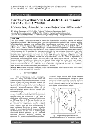
  • 1. P. Srinivasa Reddy et al. Int. Journal of Engineering Research and Application ISSN : 2248-9622, Vol. 3, Issue 5, Sep-Oct 2013, pp.845-853 RESEARCH ARTICLE www.ijera.com OPEN ACCESS Fuzzy Controller Based Seven Level Modified H-Bridge Inverter For Grid Connected PV System P.Srinivasa Reddy1,S.Shamshul Haq 2, A.Mallikarjuna Prasad 3, S.Thirumalaiah4 PG Scholar, Department of EEE, St.Johns College of Engineering, Yemmiganur, India1 Assistant Professor, Department of EEE, St.Johns College of Engineering, Yemmiganur, India 2 Associate Professor, Department of EEE, St.Johns College of Engineering, Yemmiganur, India 3,4 ABSTRACT This paper proposes a single-phase seven-level inverter for grid-connected photovoltaic systems, with a novel pulse width-modulated (PWM) control scheme. Three reference signals that are identical to each other with an offset value that is equivalent to the amplitude of the triangular carrier signal were used to generate the PWM signals. The inverter is capable of producing seven levels of output-voltage levels (Vdc, 2Vdc/3, Vdc/3, 0, −Vdc, −2Vdc/3, −Vdc/3) from the dc supply voltage. And it recounts the development of a novel modified Hbridge single-phase multilevel inverter that has two diode embedded bidirectional switches and a novel pulse width modulated (PWM) technique. The topology was applied to a grid-connected photovoltaic system with considerations for a maximum-power-point tracker (MPPT) and a current-control algorithm. Multilevel inverters offer improved output waveforms and lower THD. The circuit topology, modulation law, and operational principle of the proposed inverter were analyzed in detail. A FUZZY control is implemented to optimize the performance of the inverter. MATLAB/SIMULINK results indicate that the THD of the Fuzzy Controller Circuit is much lesser. Furthermore, both the grid voltage and the grid current are in phase at nearunity power factor. By controlling the modulation index, the desired number of levels of the inverter’s output voltage can be achieved. The less THD in the seven-level inverter compared with that in the five- and threelevel inverters is an attractive solution for grid-connected PV inverters. INDEX TERMS— Grid connected Photovoltaic system, Maximum power point tracking system, Single phase seven level inverter and fuzzy logic controller. I. INTRODUCTION The ever-increasing energy consumption, fossil fuels’ soaring costs and exhaustible nature, and worsening global environment have created a booming interest in renewable energy generation systems, one of which is photovoltaic. Such a system generates electricity by converting the Sun’s energy directly into electricity. Photovoltaic-generated energy can be delivered to power system networks through gridconnected inverters. A single-phase grid-connected inverter is usually used for residential or low-power applications of power ranges that are less than 10 kW. Types of single-phase grid-connected topology of this inverter are full-bridge three-level. The three-level inverter can satisfy specifications through its very high switching, but it could also unfortunately increase switching losses, acoustic noise, and level of interference to other equipment. Improving its output waveform reduces its harmonic content and, hence, also the size of the filter used and the level of electromagnetic interference (EMI) generated by the inverter’s switching operation. Multilevel inverters are promising; they have nearly sinusoidal output-voltage www.ijera.com waveforms, output current with better harmonic profile, less stressing of electronic components owing to decreased voltages, switching losses that are lower than those of conventional two-level inverters, a smaller filter size, and lower EMI, all of which make them cheaper, lighter, and more compact. Fig.1. Proposed single-phase seven-level Grid-connected inverter for photovoltaic systems. 845 | P a g e
  • 2. P. Srinivasa Reddy et al. Int. Journal of Engineering Research and Application ISSN : 2248-9622, Vol. 3, Issue 5, Sep-Oct 2013, pp.845-853 Various topologies for multilevel inverters have been proposed over the years. Common ones are diodeclamped, flying capacitor or multi cell, cascaded Hbridge, and modified H-bridge multilevel. This paper recounts the development of a novel modified Hbridge single-phase multilevel inverter that has two diode embedded bidirectional switches and a novel pulse width modulated (PWM) technique. The topology was applied to a grid-connected photovoltaic system with considerations for a maximum-powerpoint tracker (MPPT) and a current-control algorithm. II. PROPOSED MULTILEVEL INVERTER TOPOLOGY The proposed single-phase seven-level inverter was developed from the five-level inverter in. It comprises a single-phase conventional H-bridge inverter, two bidirectional switches, and a capacitor voltage divider formed by C1, C2, and C3, as shown in Fig. 1. The modified H-bridge topology is significantly advantageous over other topologies, i.e., less power switch, power diodes, and less capacitors for inverters of the same number of levels. Photovoltaic (PV) arrays were connected to the inverter via a dc–dc boost converter. The power generated by the inverter is to be delivered to the power network, so the utility grid, rather than a load, was used. The dc–dc boost converter was required because the PV arrays had a voltage that was lower than the grid voltage. High dc bus voltages are necessary to ensure that power flows from the PV arrays to the grid. A filtering inductance Lf was used to filter the current injected into the grid. Proper switching of the inverter can produce seven outputvoltage levels (Vdc, 2Vdc/3, Vdc/3, 0, −Vdc, −2Vdc/3, −Vdc/3) from the dc supply voltage. The proposed inverter’s operation can be divided into seven switching states, as shown in Fig. 2(a)–(g). Fig. 2(a), (d), and (g) shows a conventional inverter’s operational states in sequence, while Fig. 2(b), (c), (e), and (f) shows additional states in the proposed inverter synthesizing one- and two-third levels of the dc-bus voltage. The required seven levels of output voltage were generated as follows. 1) Maximum positive output (Vdc): S1 is ON, connecting the load positive terminal to Vdc, and S4 is ON, connecting the load negative terminal to ground. All other controlled switches are OFF; the voltage applied to the load terminals is Vdc. Fig. 2(a) shows the current paths that are active at this stage. 2) Two-third positive output (2Vdc/3): The bidirectional switch S5 is ON, connecting the load positive terminal, and S4 is ON, connecting the load negative terminal to ground. All other controlled switches are OFF; the voltage applied to the load terminals is 2Vdc/3. Fig. 2(b) shows the current paths that are active at this stage. 3) One-third positive output (Vdc/3): The bidirectional switch S6 is ON, connecting the load positive www.ijera.com www.ijera.com terminal, and S4 is ON, connecting the load negative terminal to ground. All other controlled switches are OFF; the voltage applied to the load terminals is Vdc/3. Fig. 2(c) shows the current paths that are active at this stage. 4) Zero output: This level can be produced by two switching combinations; switches S3 and S4 are ON, or S1 and S2 are ON, and all other controlled switches are OFF; terminal ab is a short circuit, and the voltage applied to the load terminals is zero. Fig. 2(d) shows the current paths that are active at this stage. 5) One-third negative output (−Vdc/3): The bidirectional switch S5 is ON, connecting the load positive terminal, and S2 is ON, connecting the load negative terminal to Vdc. All other controlled switches are OFF; the voltage applied to the load terminals is −Vdc/3. Fig. 2(e) shows the current paths that are active at this stage. 6) Two-third negative output (−2Vdc/3):The bidirectional switch S6 is ON, connecting the load positive terminal, and S2 is ON, connecting the load negative terminal to ground. All other controlled switches are OFF; the voltage applied to the load terminals is −2Vdc/3. Fig. 2(f) shows the current paths that are active at this stage. 7) Maximum negative output (−Vdc): S2 is ON, connecting the load negative terminal to Vdc, and S3 is ON, connecting the load positive terminal to ground. All other controlled switches are OFF; the voltage applied to the load terminals is −Vdc. Fig. 2(g) shows the current paths that are active at this stage. (a) (b) 846 | P a g e
  • 3. P. Srinivasa Reddy et al. Int. Journal of Engineering Research and Application ISSN : 2248-9622, Vol. 3, Issue 5, Sep-Oct 2013, pp.845-853 (c) www.ijera.com (g) Fig.2. (Continued.) Switching combination required to generate the output voltage (Vab). (e)Vab=−Vdc/3. (f)Vab = −2Vdc/3. (g) Vab = −Vdc TABLE I OUTPUT VOLTAGE ACCORDING TO THE SWITCHES’ ON–OFF CONDITION (d) Fig.2. Switching combination required to generate the output voltage (Vab). (a)Vab = Vdc. (b) Vab = 2Vdc/3. (c)Vab = Vdc/3. (d)Vab = 0. Table I shows the switching combinations that generated the seven output-voltage levels (0, −Vdc, −2Vdc/3, −Vdc/3, Vdc, 2Vdc/3, Vdc/3). (e) A novel PWM modulation technique was introduced to generate the PWM switching signals. Three reference signals (Vref1, Vref2, and Vref3) were compared with a carrier signal (Vcarrier). The reference signals had the same frequency and amplitude and were in phase with an offset value that was equivalent to the amplitude of the carrier signal. The reference signals were each compared with the carrier signal. If Vref1 had exceeded the peak amplitude of Vcarrier, Vref2 was compared with Vcarrier until it had exceeded the peak amplitude of Vcarrier. Then, onward, Vref3 would take charge and would be compared with Vcarrier until it reached zero. Once Vref3 had reached zero, Vref2 would be compared until it reached zero. (f) www.ijera.com 847 | P a g e
  • 4. P. Srinivasa Reddy et al. Int. Journal of Engineering Research and Application ISSN : 2248-9622, Vol. 3, Issue 5, Sep-Oct 2013, pp.845-853 www.ijera.com Fig.4. Seven-level output voltage (Vab) and switching angles. The phase angle depends on modulation index Ma. Theoretically, for a single reference signal and a single carrier signal, the modulation index is defined to be M a= (2) While for a single-reference signal and a dual carrier signal, the modulation index is defined to be M a= (3) Since the proposed seven-level PWM inverter utilizes three carrier signals, the modulation index is defined to be M a= Fig.3. Switching pattern for the single- phase sevenlevel inverter. Then, onward, Vref1 would be compared with Vcarrier. Fig. 3 shows the resulting switching pattern. Switches S1, S3, S5, and S6 would be switching at the rate of the carrier signal frequency, whereas S2 and S4 would operate at a frequency that was equivalent to the fundamental frequency. For one cycle of the fundamental frequency, the proposed inverter operated through six modes. Fig. 4 shows the per unit outputvoltage signal for one cycle. The six modes are described as follows: Mode 1: 0 < ωt < θ1 and θ4 < ωt < π Mode 2: θ1 < ωt < θ2 and θ3 < ωt < θ4 Mode 3: θ2 < ωt < θ3 Mode 4: π < ωt < θ5 and θ8 < ωt < 2π Mode 5: θ5 < ωt < θ6 and θ7 < ωt < θ8 Mode 6: θ6 < ωt < θ7. (4) Where Ac is the peak-to-peak value of the carrier signal and Am is the peak value of the voltage reference signal Vref . When the modulation index is less than 0.33, the phase angle displacement is θ1 =θ2 = θ3 = θ4 = (5) θ5 =θ6 = θ7 = θ8 = (6) On the other hand, when the modulation index is more than 0.33 and less than 0.66, the phase angle displacement is determined by θ1 = (7) θ2 =θ3 = (8) θ4 =π − θ1 θ5 =π + θ1 θ6 =θ7 = 3π/2 θ8 =2π − θ1 (1) (9) (10) (11) (12) If the modulation index is more than 0.66, the phase angle displacement is determined by θ1= (13) θ2= θ3 =π − θ2 www.ijera.com (14) (15) 848 | P a g e
  • 5. P. Srinivasa Reddy et al. Int. Journal of Engineering Research and Application ISSN : 2248-9622, Vol. 3, Issue 5, Sep-Oct 2013, pp.845-853 θ4 =π − θ1 θ5 =π + θ1 θ6 =π + θ2 θ7 =2π − θ2 θ8 =2π − θ1 (16) (17) (18) (19) (20) For Ma that is equal to, or less than, 0.33, only the lower reference wave (Vref3) is compared with the triangular carrier signal. The inverter’s behaviour is similar to that of a conventional full-bridge threelevel PWM inverter. However, if Ma is more than 0.33 and less than 0.66, only Vref2 and Vref3 reference signals are compared with the triangular carrier wave. The output voltage consists of five dc-voltage levels. The modulation index is set to be more than 0.66 for seven levels of output voltage to be produced. Three reference signals have to be compared with the triangular carrier signal to produce switching signals for the switches. III. CONTROL SYSTEM As Fig. 5 shows, the control system comprises a MPPT algorithm, a dc-bus voltage controller, reference-current generation, and a current controller. The two main tasks of the control system are maximization of the energy transferred from the PV arrays to the grid, and generation of a sinusoidal current with minimum harmonic distortion, also under the presence of grid voltage harmonics. The proposed inverter utilizes the perturb-and-observe (P&O) algorithm for its wide usage in MPPT owing to its simple structure and requirement of only a few measured parameters. It periodically perturbs (i.e., www.ijera.com increment or decrement) the array terminal voltage and compares the PV output power with that of the previous perturbation cycle. If the power was increasing, the perturbation would continue in the same direction in the next cycle; otherwise, the direction would be reversed. This means that the array terminal voltage is perturbed every MPPT cycle; therefore, when the MPP is reached, the P&O algorithm will oscillate around it. The P&O algorithm was implemented in the dc–dc boost converter. The output of the MPPT is the duty-cycle function. As the dc-link voltage Vdc was controlled in the dc–ac seven level PWM inverter, the change of the duty cycle changes the voltage at the output of the PV panels. The grid period and phase must be detected. The proposed inverter provides an analog zero-crossing detection circuit on one of its input ports where the grid voltage is to be connected. The zero-crossing circuit then produces an in-phase square-wave output that is fed into the digital I/O port. The feedback controller used in this application utilizes the FUZZY algorithm. The current injected into the grid, also known as grid current Igrid, was sensed and fed back to a comparator that compared it with the reference current Igridref . Igridref is the result of the MPPT algorithm. The error from the comparison process of Igrid and Igridref was fed into the controller. The output of the FUZZY controller, also known as Vref, goes through an anti windup process before being compared with the triangular wave to produce the switching signals forS1–S6.Eventually, Vref becomes Vref1; Vref2 and Vref3 can be derived from Vref1 by shifting the offset value, which was Equivalent to the amplitude of the triangular wave. Fig.5. Seven-level inverter with closed-loop control algorithm. www.ijera.com 849 | P a g e
  • 6. P. Srinivasa Reddy et al. Int. Journal of Engineering Research and Application ISSN : 2248-9622, Vol. 3, Issue 5, Sep-Oct 2013, pp.845-853 www.ijera.com Fig.(6)ATLAB SIMULINK MODEL OF MODIFIED H-BRIDGE INVERTER USING FUZZY CONTROLLER IV. A. SIMULATION AND EXPERIMENTAL RESULTS Simulation Results MATLAB SIMULINK simulated the proposed configuration before it was physically implemented in a prototype. The PWM switching patterns were generated by comparing three reference signals (Vref1, Vref2, and Vref3) against a triangular carrier signal (see Fig. 6). Subsequently, the comparing process produced PWM switching signals for switches S1–S6, as Figs. 7–9 show. One leg of the inverter operated at a high switching rate that was equivalent to the frequency of the carrier signal, while the Other leg operated at the rate of the fundamental frequency i.e. 50hz. Switches S5 and S6 also operated at the rate of the carrier signal. Fig. 10 shows the simulation result of inverter output voltage Vinv. The dc-bus voltage was set at 300 V (>√2Vgrid; in this case, Vgrid was 120 V).The dc-bus voltage must always be higher than √ 2 of Vgrid to inject current into the grid, or current will be injected from the grid into the inverter. Therefore, operation is recommended to be between Ma = 0.66 and Ma = 1.0. Vinv comprises seven voltage levels, namely, Vdc, 2Vdc/3, Vdc/3, 0, −Vdc, −2Vdc/3, and −Vdc/3. The current flowing into the grid was filtered to resemble a pure sine wave in phase with the grid voltage (see Fig. 11). As Igrid is almost a pure sine wave at unity power factor www.ijera.com Fig.7. PWM signals for S1. Fig.8. PWM signals for S2 . 850 | P a g e
  • 7. P. Srinivasa Reddy et al. Int. Journal of Engineering Research and Application ISSN : 2248-9622, Vol. 3, Issue 5, Sep-Oct 2013, pp.845-853 www.ijera.com Fig.9. PWM signals for S3. Fig.14. Grid voltage Fig.10. PWM signals for S4 Fig.15. Grid current V. Multilevel Inverter Specifications and Controller Parameters. The below table depicts the specifications and parameters of the inverter TABLEII Fig.11. PWM signals for S5 PV array rated voltage Standard Environmental Condition Solar radiation, G Cell temperature, T 1000 W/m2 25 0C System Frequency 50 Hz Switching Frequency Lb Lf C1-C3 2K Hz Inverter output voltage Fig.12. PWM signals for S6 1.2 kV 300v 2.2mh 3mh 220μF Fig.13. Inverter output voltage (Vinv). www.ijera.com 851 | P a g e
  • 8. P. Srinivasa Reddy et al. Int. Journal of Engineering Research and Application ISSN : 2248-9622, Vol. 3, Issue 5, Sep-Oct 2013, pp.845-853 VI.CONCLUSION Multilevel inverters offer improved output waveforms and lower THD. This paper has presented a novel PWM switching scheme for the proposed multilevel inverter. It utilizes three reference signals and a triangular carrier signal to generate PWM switching signals. The behaviour of the proposed multilevel inverter was analyzed in detail. a FUZZY control is implemented to optimize the performance of the inverter. By controlling the modulation index, the desired number of levels of the inverter’s output voltage can be achieved. The less THD in the sevenlevel inverter compared with that in the five- and three-level inverters is an attractive solution for gridconnected PV inverters. [9] [10] [11] REFERENCES [1] [2] [3] [4] [5] [6] [7] [8] M. Calais and V. G. Agelidis, “Multilevel converters for single-phase grid connected photovoltaic systems—An overview,” in Proc. IEEE Int. Symp. Ind. Electron., 1998, vol. 1, pp. 224–229. S. B. Kjaer, J. K. Pedersen, and F. Blaabjerg, “A review of single-phase grid connected inverters for photovoltaic modules,” IEEE Trans. Ind. Appl., vol. 41, no. 5, pp. 1292–1306, Sep./Oct. 2005. P. K. Hinga, T. Ohnishi, and T. Suzuki, “A new PWM inverter for photovoltaic power generation system,” in Conf. Rec. IEEE Power Electron. Spec. Conf., 1994, pp. 391– 395. Y. Cheng, C. Qian, M. L. Crow, S. Pekarek, and S. Atcitty, “A comparison of diodeclamped and cascaded multilevel converters for a STATCOM with energy storage,” IEEE Trans. Ind. Electron., vol. 53, no. 5, pp. 1512– 1521, Oct. 2006. M. Saeedifard, R. Iravani, and J. Pou, “A space vector modulation strategy for a backto-back five-level HVDC converter system,” IEEE Trans. Ind. Electron., vol. 56, no. 2, pp. 452–466, Feb. 2009. S.Alepuz, S.Busquets-Monge, J. Bordonau, J. A. M. Velasco, C. A. Silva, J. Pontt, and J. Rodríguez, “Control strategies based on symmetrical components for grid-connected converters under voltage dips,” IEEE Trans. Ind. Electron., vol. 56, no. 6, pp. 2162– 2173, Jun. 2009. J. Rodríguez, J. S. Lai, and F. Z. Peng, “Multilevel inverters: A survey of topologies, controls, and applications,” IEEE Trans. Ind. Electron., vol. 49, no. 4, pp. 724–738, Aug. 2002. J. Rodriguez, S. Bernet, B. Wu, J. O. Pontt, and S. Kouro, “Multilevel voltage-sourceconverter topologies for industrial medium- www.ijera.com [12] [13] [14] [15] [16] [17] [18] [19] www.ijera.com voltage drives,” IEEE Trans. Ind. Electron., vol. 54, no. 6, pp. 2930–2945,Dec. 2007. M. M. Renge and H. M. Suryawanshi, “Five-level diode clamped inverter to eliminate common mode voltage and reduce dv/dt in medium voltage rating induction motor drives,” IEEE Trans. Power Electron., vol. 23, no. 4, pp. 1598–1160, Jul. 2008. E. Ozdemir, S. Ozdemir, and L. M. Tolbert, “Fundamentalfrequencymodulated six-level diode-clamped multilevel inverter for threephase stand-alone photovoltaic system,” IEEE Trans. Ind. Electron., vol. 56, no. 11, pp. 4407–4415, Nov. 2009. R. Stala, S. Pirog, M. Baszynski, A. Mondzik, A. Penczek, J. Czekonski, and S. Gasiorek, “Results of investigation of multicell converters with balancing circuit— Part I,” IEEE Trans. Ind. Electron., vol. 56, no. 7, pp. 2610–2619, Jul. 2009. R. Stala, S. Pirog, M. Baszynski, A. Mondzik, A. Penczek, J. Czekonski, and S. Gasiorek, “Results of investigation of multicell converters with circuit—Part II,” IEEE Trans. Ind. Electron., vol. 56, no. 7, pp. 2620–2628, Jul. 2009. P. Lezana, R. Aguilera, and D. E. Quevedo, “Model predictive controlof an asymmetric flying capacitor converter,” IEEE Trans. Ind. Electron., vol. 56, no. 6, pp. 1839– 1846, Jun. 2009. M. F. Escalante, J.-C. Vannier, and A. Arzandé, “Flying capacitor multilevel inverters and DTC motor drive applications,” IEEE Trans. Ind. Electron., vol. 49, no. 4, pp. 809–815, Aug. 2002. A. Shukla, A. Ghosh, and A. Joshi, “Static shunt and series compensations of an SMIB system using flying capacitor multilevel inverter,” IEEE Trans. Power Del., vol. 20, no. 4, pp. 2613–2622, Oct. 2005. J. Huang and K. A. Corzine, “Extended operation of flying capacitor multilevel inverter,” IEEE Trans. Power Electron., vol. 21, no. 1, pp. 140–147, Jan. 2006. F. Z. Peng, “A generalized multilevel inverter topology with self voltage balancing,” IEEE Trans. Ind. Appl., vol. 37, no. 2, pp. 611–617, Mar./Apr. 2001. E. Villanueva, P. Correa, J. Rodríguez, andM. Pacas, “Control of a singlephase cascaded H-bridge multilevel inverter for grid-connected photovoltaic systems,” IEEE Trans. Ind. Electron., vol. 56, no. 11, pp. 4399– 4406, Nov. 2009. L. M. Tolbert, F. Z. Peng, T. Cunnyngham, and J. N. Chiasson, “Charge balance control schemes for cascade multilevel converter in hybrid electric vehicles,” IEEE Trans. Ind. 852 | P a g e
  • 9. P. Srinivasa Reddy et al. Int. Journal of Engineering Research and Application ISSN : 2248-9622, Vol. 3, Issue 5, Sep-Oct 2013, pp.845-853 [20] [21] [22] [23] [24] [25] [26] [27] [28] [29] [30] Electron., vol. 49, no. 5, pp. 1058–1064,Oct. 2002. K. A. Corzine, M. W. Wielebski, F. Z. Peng, and J. Wang, “Control of cascaded multilevel inverters,” IEEE Trans. Power Electron., vol. 19, no. 3, pp. 732–738, May 2004. J. I. Leon, S. Vazquez, S. Kouro, L. G. Franquelo, J. M. Carrasco, and J. Rodriguez, “Unidimensional modulation technique for cascaded multilevel converters,” IEEE Trans. Ind. Electron., vol. 49, no. 5, pp. 1058–1064, Oct. 2002. C.-C. Hua, C.-W. Wu, and C.-W. Chuang, “A digital predictive current control with improved sampled inductor current for cascaded inverters,” IEEE Trans. Ind. Electron., vol. 56, no. 5, pp. 1718–1726, May 2009. S. Vazquez, J. I. Leon, L. G. Franquelo, J. J. Padilla, and J. M. Carrasco, “DC-voltageratio control strategy for multilevel cascaded converters fed with a single DC source,” IEEE Trans. Ind. Electron., vol. 56, no. 7, pp. 2513–2521, Jul. 2009. C. Cecati, F. Ciancetta, and P. Siano, “A multilevel inverter for photovoltaic systems with fuzzy logic control,” IEEE Trans. Ind. Electron., vol. 57, no. 12, pp. 4115–4125, Dec. 2010. G. Ceglia, V. Guzman, C. Sanchez, F. Ibanez, J. Walter, and M. I. Gimanez, “A new simplified multilevel inverter topology for DC–AC conversion,” IEEE Trans. Power Electron., vol. 21, no. 5, pp. 1311– 1319, Sep. 2006. V. G. Agelidis, D. M. Baker, W. B. Lawrance, and C. V. Nayar, “A multilevel PWM inverter topology for photovoltaic applications,” in Proc. IEEE ISIE, Guimäes, Portugal, 1997, pp. 589–594. S. J. Park, F. S. Kang,M.H.Lee, and C. U. Kim, “Anewsingle-phase fivelevel PWM inverter employing a deadbeat control scheme,” IEEE Trans. Power Electron., vol. 18, no. 3, pp. 831–843, May 2003. J. Selvaraj and N. A. Rahim, “Multilevel inverter for grid-connected PV system employing digital PI controller,” IEEE Trans. Ind. Electron., vol. 56, no. 1, pp. 149–158, Jan. 2009. N. A. Rahim and J. Selvaraj, “Multi-string five-level inverter with novel PWM control scheme for PV application,” IEEE Trans. Ind. Electron., vol. 57, no. 6, pp. 2111– 2121, Jun. 2010. M. P. Kazmierkowski, R. Krishnan, and F. Blaabjerg, Control in Power Electronics Selected Problems. New York: Academic, 2002. www.ijera.com www.ijera.com BIOGRAPHIES P.SRINIVASA REDDY is doing M.Tech in Power Electronics and Drives in St.Johns College of Engineering, Yemmiganur, Kurnool District. His research interests are Power Electronics, Ac motor drives S.SHAMSHUL HAQ is the Assistant Professor in the department of EEE, St.Johns College of Engineering, Yemmiganur. He has 6 years of teaching experience. His areas of interests are Power systems, Power Electronics, Ac motor drives. A.MALLIKARJUNA PRASAD has obtained his B.E from MADRAS University in the year 2001. He has obtained his M.E from Sathyabama University in the year 2004. He has 10 years of teaching experience. Presently he is a research scholar in JNTU, KAKINADA. He is working in the area of high power density dc-dc converters S.THIRUMALAIAH has obtained his B.TECH from S.K University in the year 2002. He has obtained his M.TECH from J.N.TU HYDERABAD in the year 2008. He has 6 years of teaching experience. Presently he is a research scholar in JNTU, ANATAPUR. He is working in the area of power system control with application of power electronics. 853 | P a g e