![As a result, load terminals are short circuited by freewheeling diode FD.
Thus the load voltage is zero during TOFF period.
In this manner, a chopped DC voltage is produced across the load terminals.
The average voltage is given as follows:
The above equation shows that, the load voltage is independent of load current.
From the T=TON +TOFF equation, it is clear that the load voltage depends on two factors.
The supply voltage
The duty cycle of the chopper
Since the supply voltage is constant, load voltage is governed by the duty-cycle of the chopper.
In other words, the load voltage is dependent on two factors TON and TOFF.
Hence it is concluded that the average load voltage can be controlled by varying the value of TON and/ of TOFF in
the following two ways.
[1] Varying TON and keeping the periodic time T constant. This is called constant frequency system.
[2] Variable frequency system. ie, Keeping either TON constant and varying TOFF or keeping TOFF constant and
varying TON.
Applications of Choppers:
They are used for DC motor control (battery-supplied vehicles), solar energy conversion and wind energy conversion.
Choppers are used in electric cars, airplanes and spaceships, where onboard-regulated DC power supplies are required.
In general, Chopper circuits are used as power supplies in computers, commercial electronics, electronic instruments.
Classification of Choppers:
(a) Depending upon the direction of the output current and voltage, the converters can be classified into five classes
namely
Class A [One-quadrant Operation] (1st quadrant only)
Class B [One-quadrant Operation] (2nd quadrant only)
Class C [Two-quadrant Operation] (1,2 quadrants only)
Class D [Two-quadrant Operation] (1,4 quadrants only)
Class E [Four-quadrant Operation] (All four quadrants)
(b) Based turn off process (commutation process)
Natural Commutated Chopper ( Occurs in AC input circuits)
Forced Commutated Chopper (Occurs in DC input circuits)
The forced commutation type is further classified as
Voltage Commutated Chopper (Ex. Jones Chopper)
Current Commutated Chopper (Ex. Morgan Chopper)
(c) Based on the output voltage of the output, the choppers are classified as
(i) Step-Down Chopper
In this case the average output voltage is less than the input voltage. It is also known as step down converter](data:image/gif;base64,R0lGODlhAQABAIAAAAAAAP///yH5BAEAAAAALAAAAAABAAEAAAIBRAA7)
Empfohlen
Weitere ähnliche Inhalte
Was ist angesagt?
Was ist angesagt? (20)
Ähnlich wie Dc chopper and switching ps vr
Ähnlich wie Dc chopper and switching ps vr (20)
Kürzlich hochgeladen
Kürzlich hochgeladen (20)
Dc chopper and switching ps vr
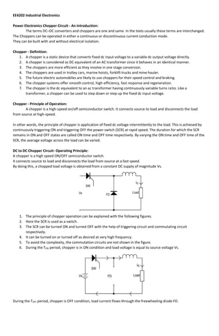
- 1. EE4202 Industrial Electronics Power Electronics Chopper Circuit - An Introduction: The terms DC–DC converters and choppers are one and same. In the texts usually these terms are interchanged. The Choppers can be operated in either a continuous or discontinuous current conduction mode. They can be built with and without electrical isolation. Chopper - Definition: 1. A chopper is a static device that converts fixed dc input voltage to a variable dc output voltage directly. 2. A chopper is considered as DC equivalent of an AC transformer since it behaves in an identical manner. 3. The choppers are more efficient as they involve in one stage conversion. 4. The choppers are used in trolley cars, marine hoists, forklift trucks and mine hauler. 5. The future electric automobiles are likely to use choppers for their speed control and braking. 6. The chopper systems offer smooth control, high-efficiency, fast response and regeneration. 7. The chopper is the dc equivalent to an ac transformer having continuously variable turns ratio. Like a transformer, a chopper can be used to step down or step up the fixed dc input voltage. Chopper - Principle of Operation: A chopper is a high-speed on/off semiconductor switch. It connects source to load and disconnects the load from source at high-speed. In other words, the principle of chopper is application of fixed dc voltage intermittently to the load. This is achieved by continuously triggering ON and triggering OFF the power switch (SCR) at rapid speed. The duration for which the SCR remains in ON and OFF states are called ON time and OFF time respectively. By varying the ON time and OFF time of the SCR, the average voltage across the load can be varied. DC to DC Chopper Circuit- Operating Principle: A chopper is a high speed ON/OFF semiconductor switch. It connects source to load and disconnects the load from source at a fast speed. By doing this, a chopped load voltage is obtained from a constant DC supply of magnitude Vs. 1. The principle of chopper operation can be explained with the following figures. 2. Here the SCR is used as a switch. 3. The SCR can be turned ON and turned OFF with the help of triggering circuit and commutating circuit respectively. 4. It can be turned on or turned off as desired at very high frequency. 5. To avoid the complexity, the commutation circuits are not shown in the figure. 6. During the TON period, chopper is in ON condition and load voltage is equal to source voltage Vs. During the TOFF period, chopper is OFF condition, load current flows through the freewheeling diode FD.
- 2. As a result, load terminals are short circuited by freewheeling diode FD. Thus the load voltage is zero during TOFF period. In this manner, a chopped DC voltage is produced across the load terminals. The average voltage is given as follows: The above equation shows that, the load voltage is independent of load current. From the T=TON +TOFF equation, it is clear that the load voltage depends on two factors. The supply voltage The duty cycle of the chopper Since the supply voltage is constant, load voltage is governed by the duty-cycle of the chopper. In other words, the load voltage is dependent on two factors TON and TOFF. Hence it is concluded that the average load voltage can be controlled by varying the value of TON and/ of TOFF in the following two ways. [1] Varying TON and keeping the periodic time T constant. This is called constant frequency system. [2] Variable frequency system. ie, Keeping either TON constant and varying TOFF or keeping TOFF constant and varying TON. Applications of Choppers: They are used for DC motor control (battery-supplied vehicles), solar energy conversion and wind energy conversion. Choppers are used in electric cars, airplanes and spaceships, where onboard-regulated DC power supplies are required. In general, Chopper circuits are used as power supplies in computers, commercial electronics, electronic instruments. Classification of Choppers: (a) Depending upon the direction of the output current and voltage, the converters can be classified into five classes namely Class A [One-quadrant Operation] (1st quadrant only) Class B [One-quadrant Operation] (2nd quadrant only) Class C [Two-quadrant Operation] (1,2 quadrants only) Class D [Two-quadrant Operation] (1,4 quadrants only) Class E [Four-quadrant Operation] (All four quadrants) (b) Based turn off process (commutation process) Natural Commutated Chopper ( Occurs in AC input circuits) Forced Commutated Chopper (Occurs in DC input circuits) The forced commutation type is further classified as Voltage Commutated Chopper (Ex. Jones Chopper) Current Commutated Chopper (Ex. Morgan Chopper) (c) Based on the output voltage of the output, the choppers are classified as (i) Step-Down Chopper In this case the average output voltage is less than the input voltage. It is also known as step down converter
- 3. (ii) Step-Up Chopper Here the average output voltage is more than the input voltage. It is also known as step up converter (iii) Step-Up/Down Chopper This type of converter produces an output voltage that is either lower or higher than the input voltage (d) Depending upon the power loss occurred during turn ON/OFF of the switching device, the choppers are classified into two categories namely (i) Hard switched Converter Here the power loss is high during the switching (ON to OFF and OFF to ON) as a result of the non zero voltage and current on the power switches. (ii) Soft switched or resonant converters In this type of choppers, the power loss is low at the time of switching as a result of zero voltage and/or zero current on the switches. Switching Power Supply and Voltage Regulators One of the disadvantages that series voltage regulators have is that, their maximum continuous output current rating is limited to just a few amperes or so, so are generally used in applications where low power outputs are required. When higher output voltage or current power supplies are required, the normal practice is to use a switching regulator commonly known as a switch-mode power supply to convert the mains voltage into whatever higher power output is required. Switch Mode Power Supplies, or SMPS, are becoming common place and have replaced in most cases the traditional linear ac-to-dc power supplies as a way to cut power consumption, reduce heat dissipation, as well as size and weight. Switch-mode power supplies can now be found in most PC’s, power amplifiers, TV’s, dc motor drives, etc., and just about anything that requires a highly efficient supply as switch-mode power supplies are increasingly becoming a much more mature technology. By definition, a switch mode power supply (SMPS) is a type of power supply that uses semiconductor switching techniques, rather than standard linear methods to provide the required output voltage. The basic switching converter consists of a power switching stage and a control circuit. The power switching stage performs the power conversion from the circuits input voltage, VIN to its output voltage, VOUT which includes output filtering. The major advantage of the switch mode power supply is its higher efficiency, compared to standard linear regulators, and this is achieved by internally switching a transistor (or power MOSFET) between its “ON” state (saturated) and its “OFF” state (cut-off), both of which produces lower power dissipation. This means that when the switching transistor is fully “ON” and conducting current, the voltage drop across it is at its minimal value, and when the transistor is fully “OFF” there is no current flow through it. So the transistor is acting like an ideal switch. As a result, unlike linear regulators which only offer step-down voltage regulation, a switch mode power supply, can offer step-down, step-up and negation of the input voltage using one or more of the three basic switch mode circuit topologies: Buck, Boost and Buck-Boost. This refers to how the transistor switch, inductor, and smoothing capacitor are connected within the basic circuit. Buck Switch Mode Power Supply The Buck switching regulator is a type of switch mode power supply circuit that is designed to efficiently reduce DC voltage from a higher voltage to a lower one, that is it subtracts or “Bucks” the supply voltage, thereby reducing the voltage available at the output terminals without changing the polarity. In other words, the buck switching regulator is a step-down regulator circuit, so for example a buck converter can convert say, +12 volts to +5 volts. The buck switching regulator is a DC-to-DC converter and one of the simplest and most popular type of switching regulator. When used within a switch mode power supply configuration, the buck switching regulator uses a series transistor or power MOSFET (ideally an insulated gate bipolar transistor, or IGBT) as its main switching device as shown below. The Buck Switching Regulator
- 4. We can see that the basic circuit configuration for a buck converter is a series transistor switch, TR1 with an associated drive circuit that keeps the output voltage as close to the desired level as possible, a diode, D1, an inductor, L1 and a smoothing capacitor, C1. The buck converter has two operating modes, depending on if the switching transistor TR1 is turned “ON” or “OFF”. When the transistor is biased “ON” (switch closed), diode D1 becomes reverse biased and the input voltage, VIN causes a current to flow through the inductor to the connected load at the output, charging up the capacitor, C1. As a changing current flows through the inductor coil, it produces a back-emf which opposes the flow of current, according to Faraday’s law, until it reaches a steady state creating a magnetic field around the inductor, L1. This situation continues indefinitely as long as TR1 is closed. When transistor TR1 is turned “OFF” (switch open) by the controlling circuitry, the input voltage is instantly disconnected from the emitter circuit causing the magnetic field around the inductor to collapse inducing a reverse voltage across the inductor. This reverse voltage causes the diode to become forward biased, so the stored energy in the inductors magnetic field forces current to continue to flow through the load in the same direction, and return back through diode. Then the inductor, L1 returns its stored energy back to the load acting like a source and supplying current until all the inductor’s energy is returned to the circuit or until the transistor switch closes again, whichever comes first. At the same time the capacitor also discharges supplying current to the load. The combination of the inductor and capacitor forms an LC filter smoothing out any ripple created by the switching action of the transistor. Therefore, when the transistor solid state switch is closed, current is supplied from the supply, and when the transistor switch is open, current is supplied by the inductor. Note that the current flowing through the inductor is always in the same direction, either directly from the supply or via the diode but obviously at different times within the switching cycle. As the transistor switch is being continuously closed and opened, the average output voltage value will therefore be related to the duty cycle, D which is defined as the conduction time of the transistor switch during one full switching cycle. If VIN is the supply voltage, and the “ON” and “OFF” times for the transistor switch are defined as: tON and tOFF, then the output voltage VOUT is given as: So the larger the duty cycle, the higher the average DC output voltage from the switch mode power supply. From this we can also see that the output voltage will always be lower than the input voltage since the duty cycle, D can never reach one (unity) resulting in a step-down voltage regulator. Voltage regulation is obtained by varying the duty cycle and with high switching speeds, up to 200kHz, smaller components can be used thereby greatly reducing a switch mode power supply’s size and weight. Another advantage of the buck converter is that the inductor-capacitor (LC) arrangement provides very good filtering of the inductor current. Ideally the buck converter should be operated in a continuous switching mode so that the inductor current never falls to zero. With ideal components, that is zero voltage drop and switching losses in the “ON” state, the ideal buck converter could have efficiencies as high as 100%. As well as the step-down buck switching regulator for the basic design of a switch mode power supply, there is another operation of the fundamental switching regulator that acts as a step-up voltage regulator called the Boost Converter. Boost Switch Mode Power Supply The Boost switching regulator is another type of switch mode power supply circuit. It has the same types of components as the previous buck converter, but this time in different positions. The boost converter is designed to increase a DC voltage from a lower voltage to a higher one, that is it adds too or “Boosts” the supply voltage, thereby increasing the available voltage at the output terminals without changing the polarity. In other words, the boost switching regulator is a step-up regulator circuit, so for example a boost converter can convert say, +5 volts to +12 volts.
- 5. We saw previously that the buck switching regulator uses a series switching transistor within its basic design. The difference with the design of the boost switching regulator is that it uses a parallel connected switching transistor to control the output voltage from the switch mode power supply. As the transistor switch is effectively connected in parallel with the output, electrical energy only passes through the inductor to the load when the transistor is biased “OFF” (switch open) as shown. The Boost Switching Regulator In the Boost Converter circuit, when the transistor switch is fully-on, electrical energy from the supply, VIN passes through the inductor and transistor switch and back to the supply. As a result, none of it passes to the output as the saturated transistor switch effectively creates a short-circuit to the output. This increases the current flowing through the inductor as it has a shorter inner path to travel back to the supply. Meanwhile, diode D1 becomes reverse biased as its anode is connected to ground via the transistor switch with the voltage level on the output remaining fairly constant as the capacitor starts to discharge through the load. When the transistor is switched fully-off, the input supply is now connected to the output via the series connected inductor and diode. As the inductor field decreases the induced energy stored in the inductor is pushed to the output by VIN, through the now forward biased diode. The result of all this is that the induced voltage across the inductor L1 reverses and adds to the voltage of the input supply increasing the total output voltage as it now becomes, VIN + VL. Current from the smoothing capacitor, C1 which was used to supply the load when the transistor switch was closed, is now returned to the capacitor by the input supply via the diode. Then the current supplied to the capacitor is the diode current, which will always be ON or OFF as the diode is continually switched between forward and reverse status by the switching actions of transistor. Then the smoothing capacitor must be sufficiently large enough to produce a smooth steady output. As the induced voltage across the inductor L1 is negative, it adds to the source voltage, VIN forcing the inductor current into the load. The boost converters steady state output voltage is given by: As with the previous buck converter, the output voltage from the boost converter depends upon the input voltage and duty cycle. Therefore, by controlling the duty cycle, output regulation is achieved. Not also that this equation is independent of the value of the inductor, the load current, and the output capacitor. We have seen above that the basic operation of a non-isolated switch mode power supply circuit can use either a buck converter or boost converter configuration depending upon whether we require a step-down (buck) or step-up (boost) output voltage. While buck converters may be the more common SMPS switching configuration, boost converters are commonly used in capacitive circuit applications such as battery chargers, photo-flashes, strobe flashes, etc, because the capacitor supplies all of the load current while the switch is closed. But we can also combine these two basic switching topologies into a single non-isolating switching regulator circuit called unsurprisingly, a Buck-Boost Converter. Buck-Boost Switching Regulator The Buck-Boost switching regulator is a combination of the buck converter and the boost converter that produces an inverted (negative) output voltage which can be greater or less than the input voltage based on the duty cycle. The buck-boost converter is a variation of the boost converter circuit in which the inverting converter only delivers the energy stored by the inductor, L1, into the load. The basic buck-boost switch mode power supply circuit is given below. The Buck-Boost Switching Regulator
- 6. When the transistor switch, TR1, is switched fully-on (closed), the voltage across the inductor is equal to the supply voltage so the inductor stores energy from the input supply. No current is delivered to the connected load at the output because diode, D1, is reverse biased. When the transistor switch is fully-off (open), the diode becomes forward biased and the energy previously stored in the inductor is transferred to the load. In other words, when the switch is “ON”, energy is delivered into the inductor by the DC supply (via the switch), and none to the output, and when the switch is “OFF”, the voltage across the inductor reverses as the inductor now becomes a source of energy so the energy stored previously in the inductor is switched to the output (through the diode), and none comes directly from the input DC source. So the voltage dropped across the load when the switching transistor is “OFF” is equal to the inductor voltage. The result is that the magnitude of the inverted output voltage can be greater or smaller (or equal to) the magnitude of the input voltage based on the duty cycle. For example, a positive-to-negative buck-boost converter can convert 5 volts to 12 volts (step-up) or 12 volts to 5 volts (step-down). The buck-boost switching regulators steady state output voltage, VOUT is given as: Then the buck-boost regulator gets its name from producing an output voltage that can be higher (like a boost power stage) or lower (like a buck power stage) in magnitude than the input voltage. However, the output voltage is opposite in polarity from the input voltage. Switch Mode Power Supply Summary The modern switch mode power supply, or SMPS, uses solid-state switches to convert an unregulated DC input voltage to a regulated and smooth DC output voltage at different voltage levels. The input supply can be a true DC voltage from a battery or solar panel, or a rectified DC voltage from an AC supply using a diode bridge along with some additional capacitive filtering. In many power control applications, the power transistor, MOSFET or IGFET, is operated in its switching mode were it is repeatedly turned “ON” and “OFF” at high speed. The main advantage of this is that the power efficiency of the regulator can be quite high because the transistor is either fully-on and conducting (saturated) or full-off (cut-off). There are several types of DC-to-DC converter (as opposed to a DC-to-AC converter which is an inverter) configurations available, with the three basic switching power supply topologies looked at here being the Buck, Boost, and the Buck-Boost switching regulators. All three of these topologies are non-isolated, that is their input and output voltages share a common ground line. Each switching regulator design has its own unique properties with regards to the steady-state duty cycles, relationship between the input and output current, and the output voltage ripple produced by the solid-state switch action. Another important property of these switch mode power supply topologies is the frequency response of the switching action to the output voltage. Regulation of the output voltage is achieved by the percentage control of the time that the switching transistor is in the “ON” state compared to the total ON/OFF time. This ratio is called the duty cycle and by varying the duty cycle, (D the magnitude of the output voltage, VOUT can be controlled. The use of a single inductor and diode as well as fast switching solid-state switches capable of operating at switching frequencies in the kilohertz range, within the switch mode power supply design, allows for the size and weight of the power supply to be greatly reduced. This is because there would be no large and heavy step-down (or step-up) voltage mains transformers within their design. However, if isolation is required between the input and output terminals, a transformer must be included before the converter. The two most popular non-isolated switching configurations are the buck (subtractive) and the boost (additive) converters.
- 7. The buck converter is a type of switch-mode power supply that is designed to convert electrical energy from one voltage to a lower one. The buck converter operates with a series connected switching transistor. As the duty cycle, D < 1, the output voltage of the buck is always smaller than the input voltage, VIN. The boost converter is a type of switch-mode power supply that is designed to convert electrical energy from one voltage to a higher one. The boost converter operates with a parallel connected switching transistor which results in a direct current path between VIN and VOUT via the inductor, L1 and diode, D1. This means there is no protection against short-circuits on the output. By varying the duty cycle, (D) of a boost converter, the output voltage can be controlled and with D < 1, the DC output from the boost converter is greater than input voltage VIN as a consequence of the inductors self-induced voltage. Also, the output smoothing capacitors in Switch-mode Power Supplies is assumed to be very large, which results in a constant output voltage from the switch mode supply during the transistors switching action.