PillarHall basic concept SlideShare
•
1 gefällt mir•1,274 views

Basic concept of PillarHall thin film conformality analysis explained. http://www.pillarhall.com

Empfohlen
Empfohlen
Weitere ähnliche Inhalte
Was ist angesagt?
Was ist angesagt? (20)
Andere mochten auch
Andere mochten auch (20)
Ähnlich wie PillarHall basic concept SlideShare
Ähnlich wie PillarHall basic concept SlideShare (20)
Mehr von Riikka Puurunen
Mehr von Riikka Puurunen (9)
Kürzlich hochgeladen
Kürzlich hochgeladen (20)
PillarHall basic concept SlideShare
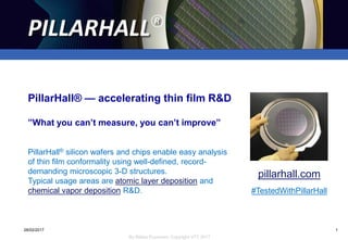
- 1. 1 By Riikka Puurunen, Copyright VTT 2017 PillarHall® 09/05/2017 1 PillarHall® silicon wafers and chips enable easy analysis of thin film conformality using well-defined, record- demanding microscopic 3-D structures. Typical usage areas are atomic layer deposition and chemical vapor deposition R&D. pillarhall.com #TestedWithPillarHall PillarHall® — accelerating thin film R&D ”What you can’t measure, you can’t improve”
- 2. 2 By Riikka Puurunen, Copyright VTT 2017 PillarHall® 09/05/2017 2 Conformal film covers complex 3-D structures uniformly with the same thickness and properties Conformal film, schematic example: a. Optimized ALD Same film top (1), sidewall (2), bottom (3), deep within (4) Partly conformal & non-conformal films, schematic examples b. Partly conformal, typical for CVD c. Noncormal with overhang, from line-of-sight deposition d. ”Superconformal”, i.e., preferential filling inside the 3-D feature (a) (c) (d)(b) (Side view) 1. 2. 3.4.
- 3. 3 By Riikka Puurunen, Copyright VTT 2017 PillarHall® 09/05/2017 3 Traditional way of measuring conformality: Cross-sections of vertical trenches in silicon • Measurement takes time & effort, accuracy operator-dependent • Point-per-point analysis, wafer mapping quasi-impossible Vertical HAR procedure: Measure thickness 1. Top 2. Sidewall 3. Bottom Calculate conformality: • Bottom/top xx% • Sidewall/top yy% Aspect ratio (height/width, not in scale) max ~50:1 1. 2. 3. If thinner in trench conformality <100%
- 4. 4 By Riikka Puurunen, Copyright VTT 2017 PillarHall® 09/05/2017 4 Schematic: uncoated structure Structure after coating with ALD, CVD, … Structure after peeling off the top membrane PillarHall® lateral high-aspect-ratio (LHAR) all-silicon chips and wafers (current: 150 mm)
- 5. 5 By Riikka Puurunen, Copyright VTT 2017 PillarHall® 09/05/2017 5 Typical 500 nm Max 5000 µm Max 5000 µm Top view Side view ~1.5 µm PillarHall® dimensions (not in scale) • Gap height typically 500 nm, can be varied (e.g., 100 and 1000 nm) • Membrane length up to 5000 µm • Multiple aspect ratios (AR) in one chip, e.g. 5:1 to 10 000:1
- 6. 6 By Riikka Puurunen, Copyright VTT 2017 PillarHall® 09/05/2017 6 PillarHall®: Multitude of analysis possibilities Penetration depth under membrane ~70 µm AR ~140:1 Cross-section, SEM (50 nm by ALD) For scientific publications, see DOI 10.1116/1.4903941; DOI acs.langmuir.6b03007 More info to come: Puurunen et al., EuroCVD 2017, accepted; ALD 2017, submitted Top-view microscopy (50 nm by ALD) Quick semiquantitative (nondestructive) analysis Traditional electron microscopy cross-sections Uniform coating all around the feature, AR ~40:1, gap height 500 nm
- 7. 7 By Riikka Puurunen, Copyright VTT 2017 PillarHall® 09/05/2017 7 PillarHall®: Remove top membrane to access detailed, reproducible information of film on Si Photo: Riikka Puurunen, VTT Distance from LHAR opening (µm) Reflectometry Al2O3 ALD For scientific publications, see: DOI 10.1116/1.4903941; DOI acs.langmuir.6b03007 More info to come: Puurunen et al., EuroCVD 2017, accepted; ALD 2017, submitted
- 8. 8 By Riikka Puurunen, Copyright VTT 2017 PillarHall® 09/05/2017 8 distance, aspect ratio thickness • Optimise reaction times/doses (tA, tB, pA, pB) • Extract kinetic parameters • Optimise purge times (tA2, tB2) • Understand reaction mechanisms PillarHall® line scans: route to understanding and optimising process fundamentals
- 9. 9 By Riikka Puurunen, Copyright VTT 2017 PillarHall® 09/05/2017 9 PillarHall®: Some benefits Avoid the need for tedious cross-sections combined with electron microscopy, needed for traditional vertical features Record-high aspect ratios >10000:1, exposing a parameter space beyond access with traditional vertical structures Microscopic dimensions suitable for kinetic modelling Wafer mapping possibility, even nondestructively IC-compatible wafers. Potentially chips , too Applicable at temperatures up to ~800°C
- 10. 10 By Riikka Puurunen, Copyright VTT 2017 PillarHall® 09/05/2017 10 Scientific publications using PillarHall 1st generation prototypes 1. Microscopic silicon-based lateral high-aspect-ratio structures for thin film conformality analysis, F. Gao, S. Arpiainen, R. L. Puurunen, J. Vac. Sci. Technol. A 33 (2015) 010601. http://dx.doi.org/10.1116/1.4903941, open access pdf. 2. Nucleation and Conformality of Iridium and Iridium Oxide Thin Films Grown by Atomic Layer Deposition, M. Mattinen, J. Hämäläinen, F. Gao, P. Jalkanen, K. Mizohata, J. Räisänen, R. L. Puurunen, M. Ritala, M. Leskelä, Langmuir 32 (2016) 10559-10569. http://dx.doi.org/10.1021/acs.langmuir.6b03007 3. Influence of ALD temperature on thin film conformality: Investigation with microscopic lateral high-aspect-ratio structures, R. L. Puurunen, F. Gao, Proceedings of the International Baltic Conference on Atomic Layer Deposition, 2-4 Oct 2016, St. Petersburg, Russia. Electronically published in IEEE Xplore, http://ieeexplore.ieee.org/document/7886526/
- 11. 11 By Riikka Puurunen, Copyright VTT 2017 PillarHall® 09/05/2017 11 Interested to know more on PillarHall®? Take the PillarHall Survey Contact Mikko Utriainen, Tel: +358 40 753 7415, pillarhall (at) vtt.fi Participate in PillarHall survey Proof-of-concept tests with selected partners interested parties can contact Meet us at conferences: Joint EuroCVD 21 - Baltic ALD 15, June 11-14, 2017, Linköping, Sweden, http://www.eurocvd-balticald2017.se/ ALD 2017, 17th International Conference on Atomic Layer Deposition, Denver, Colorado, USA, July 15-18, 2017. https://aldconference.avs.org/. Dr. Mikko Utriainen Prof. Riikka Puurunen
- 12. 12 By Riikka Puurunen, Copyright VTT 2017 PillarHall® 09/05/2017 12 PillarHall® — Accelerating thin film R&D http://www.pillarhall.com Email: pillarhall (at) vtt.fi Twitter: #TestedWithPillarHall