counter using 4 master slave flip-flops
•Als DOCX, PDF herunterladen•
3 gefällt mir•8,585 views

This document describes how to design a 4-bit counter using master-slave JK flip-flops. It begins by explaining what a flip-flop is and describing common flip-flop types like the SR, JK, and master-slave JK flip-flop. It then shows how to connect 4 master-slave JK flip-flops in a ring configuration to form a counter that will count from 0 to 15 (hexadecimal F). The document concludes by presenting the circuit design of a 4-bit counter created using DSCH simulation software, along with output waveforms and a timing diagram verifying the counter operates as intended.

Empfohlen
Weitere ähnliche Inhalte
Was ist angesagt?
Was ist angesagt? (20)
Andere mochten auch
Ähnlich wie counter using 4 master slave flip-flops
Ähnlich wie counter using 4 master slave flip-flops (20)
Mehr von ZunAib Ali
Mehr von ZunAib Ali (20)
counter using 4 master slave flip-flops
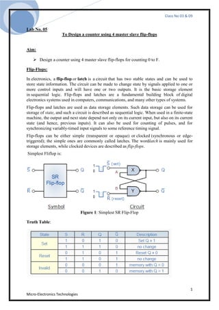
- 1. Class No 03 & 09 Lab No. 05 To Design a counter using 4 master slave flip-flops Aim: Design a counter using 4 master slave flip-flops for counting 0 to F. Flip-Flops: In electronics, a flip-flop or latch is a circuit that has two stable states and can be used to store state information. The circuit can be made to change state by signals applied to one or more control inputs and will have one or two outputs. It is the basic storage element in sequential logic. Flip-flops and latches are a fundamental building block of digital electronics systems used in computers, communications, and many other types of systems. Flip-flops and latches are used as data storage elements. Such data storage can be used for storage of state, and such a circuit is described as sequential logic. When used in a finite-state machine, the output and next state depend not only on its current input, but also on its current state (and hence, previous inputs). It can also be used for counting of pulses, and for synchronizing variably-timed input signals to some reference timing signal. Flip-flops can be either simple (transparent or opaque) or clocked (synchronous or edge- triggered); the simple ones are commonly called latches. The wordlatch is mainly used for storage elements, while clocked devices are described as flip-flops. Simplest Fliflop is: Figure 1: Simplest SR Flip-Flop Truth Table: 1 Micro-Electronics Technologies
- 2. Class No 03 & 09 The JK Flip-flop This simple JK flip-Flop is the most widely used of all the flip-flop designs and is considered to be a universal flip-flop circuit. The sequential operation of the JK flip-flop is exactly the same as for the previous SR flip-flop with the same "set" and "reset" inputs. The difference this time is that the JK flip-flop has no invalid or forbidden input states of the SR Latch (when S and R are both 1). The JK flip-flop is basically a gated SR flip-flop with the addition of a clock input circuitry that prevents the illegal or invalid output condition that can occur when both inputs S and R are equal to logic level "1". Due to this additional clocked input, a JK flip-flop has four possible input combinations, "logic 1", "logic 0", "no change" and "toggle". The symbol for a JK flip-flop is similar to that of an SR Bistable Latch as seen in the previous tutorial except for the addition of a clock input. Figure 2: JK Flip-Flop The main defect is toggling so this can be overcome by making JK flip-flop edge triggered flip-flop & to do so we use MASTER-SLAVE Flip-Flop (the output toggle at clock trigging High-Low point of clock only) Truth Table: 2 Micro-Electronics Technologies
- 3. Class No 03 & 09 The Master-Slave JK Flip-flop (Edge Trigged Flip-Flop): The Master-Slave Flip-Flop is basically two gated SR flip-flops connected together in a series configuration with the slave having an inverted clock pulse. The outputs from Q and Q from the "Slave" flip-flop are fed back to the inputs of the "Master" with the outputs of the "Master" flip-flop being connected to the two inputs of the "Slave" flip-flop. This feedback configuration from the slave's output to the master's input gives the characteristic toggle of the JK flip-flop as shown below. Figure 3: Master Slave Flip-Flop The input signals J and K are connected to the gated "master" SR flip-flop which "locks" the input condition while the clock (Clk) input is "HIGH" at logic level "1". As the clock input of the "slave" flip-flop is the inverse (complement) of the "master" clock input, the "slave" SR flip-flop does not toggle. The outputs from the "master" flip-flop are only "seen" by the gated "slave" flip-flop when the clock input goes "LOW" to logic level "0". When the clock is "LOW", the outputs from the "master" flip-flop are latched and any additional changes to its inputs are ignored. The gated "slave" flip-flop now responds to the state of its inputs passed over by the "master" section. Then on the "Low-to-High" transition of the clock pulse the inputs of the "master" flip-flop are fed through to the gated inputs of the "slave" flip-flop and on the "High-to-Low" transition the same inputs are reflected on the output of the "slave" making this type of flip-flop edge or pulse-triggered. Then, the circuit accepts input data when the clock signal is "HIGH", and passes the data to the output on the falling-edge of the clock signal. In other words, the Master-Slave JK Flip- flop is a "Synchronous" device as it only passes data with the timing of the clock signal. Ring Counter: A ring counter is a digital circuit which consists of a series of flip flops connected together in a feedback manner. The circuit is special type of shift register where the output of the last flip-flop is fed back to the input of first flipflop.When the circuit is reset, except one of the flip-flop output, all others are made zero. For n-flip-flop ring counter we have a MOD-n counter. That means the counter has n different states. The block diagram for a 4 bit ring counter is shown below: 3 Micro-Electronics Technologies
- 4. Class No 03 & 09 Figure 4: Block Diagram of 4-bit Counter. Task: Making Counter In Software: Apparatus: DSCHV2-7 installed PC. Procedure: First of all open the software by clicking on-to the icon . For the specific gate select the required components by clicking the symbol library icon . DSCHV2-7 software includes a comprehensive block library, from this library “pmos, nmos, ground, dc source (vdd), button, led (to see the output) “can be selected to draw the circuit just by click-and-drag operations. To draw the lines between the components click on-to the icon & then join the two components by simple drag operation. The components attributes can be changed by double clicking on-to the component there by changing the required field. After completing the circuit diagram simulate the circuit by clicking . Finally, click to see the timing diagram to verify the truth table. Components used: NAND Gate Push Buttons as logic state. Ground Output leds Invertors 4 Micro-Electronics Technologies
- 5. Class No 03 & 09 Circuit Diagram: Figure 5: 4-Bit Jk Flip-Flop Counter Circuit Some Outputs Shown: Fig A: 5 Micro-Electronics Technologies
- 6. Class No 03 & 09 Fig B: Fig C: 6 Micro-Electronics Technologies
- 7. Class No 03 & 09 Timing Diagram: Figure 6 : Timing diagram Conclusion: From timing diagram it is verified that the counter counted from 0 up to F i-e 4-bit counter. Hence it is verified that the JK Flip-Flop can be used in combination for counting. 7 Micro-Electronics Technologies