SlideShare ist ein Scribd-Unternehmen logo
1 von 66
Downloaden Sie, um offline zu lesen
VLSI Design Lab


Quiescent Current Testing of CMOS
         Data Converters
                     Research Presentation
                              By
                     Siva Yellampalli

       Date: November 5, 2008 (2:00 – 4:00 PM), Fall 2008
                         Room: EE117
       Department of Electrical and Computer Engineering
                  Louisiana State University
VLSI Design Lab


      Outline of the Presentation
IDDQ Testing methodology
Testing data converter circuits
Physical faults d fault injection technique
Ph i l f lt and f lt i j ti t h i
Future trends of IDDQ testing
Circuit under test
BICS for IDDQ testing
BICS for ΔIDDQ testing
Combined IDDQ, IDDT and oscillation test methodology
                                         methodology.
IDDT current testing
Oscillation based testing
Conclusion
C     li
VLSI Design Lab


      Outline of the Presentation
IDDQ Testing Methodology
Need for Testing Data Converter Circuits
Physical Faults and Fault Injection Technique
IDDQ BICS Design
Future trends of IDDQ testing
ΔIDDQ BICS Testing
Combined IDDQ, IDDT and Oscillation Test Methodology
IDDT Current Testing
Oscillation Testing
Conclusion
VLSI Design Lab


                IDDQ Testing Methodology
          VDD                     VDD


                IDDQ=0
                                   Q3
          Q1

                                         Vout
                                         V
Vin


          Q2                        Q4


                                                With fault
                  Without fault
VLSI Design Lab


  Block Diagram of IDDQ Testing
                            VDD


                            PMOS
                           BLOCK

                  INPUTS

                                   OUTPUT

                            NMOS
                           BLOCK
                  CUT


                                     PASS/FAIL

                            BICS


                             VSS
VLSI Design Lab


 Need for Testing of Data Converter
               Circuits
Photolithographic process
Particle related defects have been observed as major
cause of defects in mixed signal circuits.
         fd f t i     i di      l i it

Physical failures
   -bridges
    -opens and
    -gate oxide shorts (GOS)
     gate              (GOS).
VLSI Design Lab


                                   Bridging Faults
                            VDD


                                                           Bridging faults
                                                            -short circuit faults in
                                                              integrated circuits.
                                                              it      t d i it
                                                            -can appear either at the
                                                              logical output of a g
                                                                g        p         gate or at
                                  V0
                                                              the transistor nodes internal
VA
                                                              to a gate.
     Bridge 1: Drain-gate


                                                VB
 Bridge 3 : Drain-source


                                  Bridge 2 : Gate-source
                                             Gate source
VLSI Design Lab


                                 Bridging Faults
                                 B id i F l
                                                           Different bridging faults*: (a)
                                                           shorting of seven metal
                                                           lines caused by unexposed
                                                           photo resist, (b) shorting of
                                                           four metal lines by solid
                                                           state particle on the metal
                                                           mask, (c) shorts and breaks
                                                           of metal lines caused by
                                                           scratch in the photo resist,
                                                           (d) short among multiple
                                                           metal lines by a
                                                           metallization defect of 1um
                                                           in size, (e) short between
                                                           two aluminum lines due to
                                                           metallization defects, and
                                                           (f) inter layer short between
                                                           two aluminum interconnects
                                                           in 0 5 um technology
                                                              0.5      technology.
*R. Rajsuman, “IDDQ testing for CMOS VLSI,” Proc. of the
IEEE, vol. 88, no. 4, 2000, pp. 544-566.
VLSI Design Lab


                                        Gate Oxide Faults
                                                                         Gate oxide shorts
                                                                           -occur frequently in CMOS
                                                                             technology.
                                                                           -reasons are breakdown of the
                                                                            gate oxide and th manufacturing
                                                                               t     id   d the       fti
                                                                            spot defects in lithography and
                                                                            processes on the active area and
                                                                            polysilicon masks
                                                                                        masks.

                                                                               Gate Oxide defects: (a) gate-
                                                                               oxide short to N+ diffusion*, and
                                                                               (b) gate oxide pin hole causing
                                                                               cell word line leakage memory+ .
*C.F. Hawkins and J.M. Soden, “Reliability and electrical properties of gate oxide shorts in CMOS ICs,” Proc. Int. Test Conf., 1986, pp. 443- 451.


+A. Chan, D. Lam, W. Tan and S.Y. Khim, “Electrical failure analysis in high density DRAMs,” Proc. Int. Test Conf., 1998, pp. 43-52.
VLSI Design Lab


                                                  Open Faults

                                                                    (a) a foreign particle causing a line
                                                                        open and a ling thinning*
                                                                    (b) A contaminated particle causing 7-
                                                                                                        7
                                                                        line opens* and
                                                                    (c) SEM picture of defect which
                                                                        caused open in metal 2 and a short
                                                                                  p
                                                                        in metal 1+.


*W. Maly, “Realistic fault modeling for VLSI testing,” IEEE Design Auto. Conf., 1987, pp. 173-180.
+J. Khare, S. Griep, H.D. Oberle, W.Maly, D.S. Landsiedel, U. Kollmer and D. M. H. Walker, “Key attributes of an SRAM testing strategy required for
effective process monitoring,” IEEE Int. workshop on Memory Testing, 1993, pp. 84-89.
VLSI Design Lab

     Fault Injection Technique
Example: Fault-Injection Transistor (N-
    MOSFET) at Inverter Output
                                 VDD


            VE
                    G


          ME                VI                        V0
                        S
D                                      D
        (4.5/1.6)
                                                      (4.5/1.6)
                                             ME            VE
                                                  G


                                       S

                                                       FIT
                                       VSS
VLSI Design Lab


      Outline of the Presentation
IDDQ Testing methodology
Need for Testing data converter circuits
Physical faults d fault injection technique
Ph i l f lt and f lt i j ti t h i
IDDQBICS design
Future trends of IDDQ testing
                            g
BICS for ΔIDDQ testing
IPS current testing
Oscillation based testing
Conclusion
VLSI Design Lab


      Outline of the Presentation
IDDQ Testing Methodology
Need for Testing Data Converter Circuits
Physical Faults and Fault Injection Technique
IDDQ BICS Design
Future trends of IDDQ testing
ΔIDDQ BICS Testing
Combined IDDQ, IDDT and Oscillation Test Methodology
IDDT Current Testing
Oscillation Testing
Conclusion
VLSI Design Lab

                                                              VDD(+2.5V)
                                                                  XFIT 3
                       M8                              M5
                                                                      VE3                  XFIT6
                                             XFIT 2                                                      M7
                                                                                          VE6
                                                            VSS
                                                                                                   VSS
                                                 VE2
                                      VSS
    CMOS Amplifier
       (CUT)
                                                                                                            VOUT
                                     M1                             M2
                                                                                           VE5 XFIT 5
                                                                         V+
                                 -
                             V
                                                                              VBIAS
                                                                      M11 (XFIT8)           VSS CC
                       M10
         XFIT 1                                                                                          M6
                                                                         VSS
                                            M3                 M4
                                                                                            VE7
                                                                            VE4
         VE1
                                                                                                   XFIT 7
                                                                     XFIT 4
                                                      VSS(-2.5V)

                             VDD

      BICS                                                                    VDD
                       5.6/1.6
                                     M5
                                                                                 11.6/1.6
                                                                         M6                     VDD
                         VSS
                                                 IDEF
                                      IREF                     EXT                  VSS               6.4/1.6
                                                                IDEF - IREF                           OUTPUT
                                              IREF
                                     36/1.6                                                               ( PASS/ FAIL )
                                                                            M4
              92/1.6                                                                                  3.2/1.6
                                     M1                        M3
                                                      M2
                        M0                             100/1.6
          VENABLE                                                                     400/1.6 VSS
                                                     36/1.6


                                                       VSS(-2.5V)
VLSI Design Lab


Simulated
Si l t d BICS O t t and M
              Output d Measured IDDQ f
                              d      for
                Defects
VLSI Design Lab


Layout of Built-in Current Sensor
VLSI Design Lab


BICS Showing PASS/FAIL Output from HP1660CS Logic
Analyzer Corresponding to Fault M5DSS
VLSI Design Lab


        Future Trends of IDDQ Testing
The theoretical basis of IDDQ testing is based upon estimation of
defect-free
defect free current in the circuit and then setting a limit
(threshold) above which a circuit is considered defective.

Methods for tti threshold limit
M th d f setting th h ld li it
 - 1μA is considered defect free any number from as low as 10
   μA to 100 μA is considered as threshold limit.
 - Due to large number of devices, the distribution of the
   measured current is expected to be Guassian. Due to
   statistical variations IC’s up to mean +3σ are considered
               variations, IC s
   defect free. A limit higher than mean +3σ is assumed, above
   which IC’s are considered defective.
VLSI Design Lab


     Future Trends of IDDQ Testing
When the density of the defect free and defective current
                           defect-free
are separated from each other, clear distinction between
the good and the defective ICs can be made.
In submicron CMOS technology the mean of the
distribution of defect free current increases and
approaches the IDDQ threshold limit (set from earlier
technology)
Changing the threshold limit to higher number does not
resolve the issue because with high leakage current the
change in defect-free and defective current is miniscule
and unidentifiable.
VLSI Design Lab


     Future Trends of IDDQ Testing

Sub threshold leakage current.

                       ⎛ Vgs −Vth ⎞ ⎛       ⎛ Vds ⎞ ⎞
                       ⎜          ⎟⎜        ⎜
                                            ⎜ v ⎟⎟
                       ⎜ S / ln10 ⎟               ⎟
                = k exp⎝          ⎠ ⎜1 − exp⎝ t ⎠ ⎟
        I sub
                                   ⎜               ⎟
                                   ⎜               ⎟
                                   ⎝               ⎠
VLSI Design Lab


      Future Trends of IDDQ T ti
      Ft     Tdf            Testing
Design Methods
D i M th d
 - Reduced temperature
 - Substrate bias
 - Switched source impedance leakage reduction
   technique
 - Dual threshold method
Testing methods
 - ΔIDDQ Testing
 - Power supply current testing
 - Oscillation testing method
VLSI Design Lab


      Future Trends of IDDQ Testing
ΔIDDQ Testing of CMOS ICs
  - relative methods of the offstate current is taken instead of
    absolute ones for fault detection.
Power supply current based testing method.
           pp y                     g
  -variation of AC ripple in the supply current under the
   application of AC input stimulus is used for fault detection.
Oscillation based t ti method.
O ill ti b       d testing     th d
- Converting the CUT is into an oscillator using feedback.
- Output oscillation frequency is monitored for faults in the
   CUT.
- Needs no test signal generation, uses simple measurement
   and has high fault coverage.
VLSI Design Lab


      Outline of the Presentation
IDDQ Testing methodology
Testing data converter circuits
Physical faults d fault injection technique
Ph i l f lt and f lt i j ti t h i
Future trends of IDDQ testing
Circuit under test
BICS for IDDQ testing
BICS for ΔIDDQ testing
IDDT current testing
Oscillation based testing
Conclusion
VLSI Design Lab


      Outline of the Presentation
IDDQ Testing Methodology
Need for Testing Data Converter Circuits
Physical Faults and Fault Injection Technique
IDDQ BICS Design
Future trends of IDDQ testing
ΔIDDQ BICS Testing
Combined IDDQ, IDDT and Oscillation Test Methodology
IDDT Current Testing
Oscillation Testing
Conclusion
VLSI Design Lab


      ∆IDDQ BICS Design and Testing
          VDD
                TG1
VTG
                          Discharging
                             input to
                           comparator                     4-Bit Binary
                          Discharging            Comp.
                                                          Synchronous
                                                           y
                          Input to               output                4-Bit
                                                Comp      Counter
                          Comparator             pulse                 Output
                                                Output
                    TG2                                                Count 1
                                                Pulse
                                                                      A
                                                                            1
                                                                      B
                                       Analog
                                            g
                                                          I/P
                                       Comp                                 0
                                                                      C
                C
CUT                                                                         0
                                                                       D
       I DDQ
                                                                CLK I/P

                                 Vref
VLSI Design Lab


                  Layout of BICS
VLSI Design Lab


                          Comparator Design
                                       VDD = 2.5V
                                                                       3/0.6      3/0.6
                                                                  M8     M10        M12
 6.6/0.6               6.6/0.6
                                                        5.4/0.6

             M3   M4

                                                                                          V OUT
                  N2
                                                        N
        N1
                                                              Inv1
                                    0.9/0.6
                                    0 9/0 6   0.9/0.6
                                              0 9/0 6
V NEG                       V POS
             M1   M2

  30/0.6               30/0.6        M5            M6          M9       M11        M13
                                                            3.9/0.6     1.5/0.6    1.5/0.6


                                    12/0.6
                                              M7


                                        GND
VLSI Design Lab


    Analog-to-Digital Converter
VLSI Design Lab


    Analog-to-Digital Converter
VLSI Design Lab


                  3-BIT Flash Architecture ADC
2.5v

                                                     3 BIT
                                                     3-BIT flash architecture
       1.5R


                                                     based ADC.
                                                     Designed for operation at
        R


                                                     2.5
                                                     2 5 V in 0 5 μm n well
                                                              0.5     n-well
        R


                                                     CMOS technology.
                                    Output Digital

                                                     The various blocks are
                                    word
        R
                         N
                        2 -1 to N
                         encoder


                                                       - voltage reference
       R


                                                       - resister ladder
                                                       - seven comparators
        R


                                                       - 8:3 encoder
        R


           0.5R
VLSI Design Lab


          3-BIT Charge Scaling Architecture DAC
                                                                 Designed for operation at
                                                                 2.5 V.
                                                          VOUT
                                                                 Building Blocks:
                                                                        g
                    2pF        1pF        0.5pF
                                             p
Reset
R                                                 0.5pF
                                                  05 F
                                                                   - Voltage Reference
                                                                   - Binary Switches
                                                                   - Scaling Network
               D2         D1         D0
                                                                   -O
                                                                    Operational Amplifier
                                                                         ti   l A lifi
  VReference
VLSI Design Lab


        Low Voltage Operational Amplifier
                    Design
                                              Double Ended
  Bulk Driving                                                                                         Second
                 Biasing Differential         to Single Ended                     High Swing
                                                                                                       Stage
  Circuitry      Circuitry Input Stage        Conversion Stage                    Circuitry            (Class A
                                                                                                       Amplifier)
                                                      VDD
                                                                                                  VON + VT
                                   M3
M17
                                                                       M21
                                             VON                                  2VON +VT
                 M15                    M4                                                                   M14
       M19
                                                                                               M12
                                                                            M23
                                                     VON +VT                                M11
                                   M1 M2
                 Mb                           VPOS
                                                     M6
                            VNEG                            M7
                                                                                                              VOUT
                                                                                            MR       Cc

                                                                 M9
                                   M5          M8                     M22
      M20
                                                                                      M10                    M13

                      M16
M18


                      Note: For the P-MOSFETS the substrate is connected to VDD
VLSI Design Lab


             Layout of Op-Amp
VLSI Design Lab

 12 bit
 12-bit ADC with Induced Faults
VLSI Design Lab


Simulation of the Comparator With no Fault
VLSI Design Lab


 Chip layout of 12 bit ADC in 40 pin
                12-bit        40-pin
             Padframe
VLSI Design Lab


Microphotograph of Fabricated Chip


  Part of 12-bit ADC
                          ΔIDDQ BICS
VLSI Design Lab


           Experimental Results
VLSI Design Lab

Simulated Count Values from SPICE and
  Experimental Values for all the Five
                Faults
VLSI Design Lab


              Equivalent Faults
                                  VDD

                      FIT                      FIT
                            M17         M19


                       R                        R


                                                     OUTPUT
             INPUT


                                               FIT
                     FIT

                            M18         M20

                                                R
                      R


                                  VSS


                                  VSUBSTRATE


                     Low Voltage op-amp.
VLSI Design Lab


                                              Double Ended
  Bulk Driving                                                                                         Second
                 Biasing Differential         to Single Ended                     High Swing
                                                                                                       Stage
  Circuitry      Circuitry Input Stage        Conversion Stage                    Circuitry            (Class A
                                                                                                       Amplifier)
                                                      VDD
                                                                                                  VON + VT
                                   M3
M17
                                                                       M21
                                             VON                                  2VON +VT
                 M15                    M4                                                                   M14
       M19
                                                                                               M12
                                                                            M23
                                                     VON +VT                                M11
                                   M1 M2
                 Mb                           VPOS
                                                     M6
                            VNEG                            M7
                                                                                                              VOUT
                                                                                            MR       Cc

                                                                 M9
                                   M5          M8                     M22
      M20
                                                                                      M10                    M13

                      M16
M18


                      Note: For the P-MOSFETS the substrate is connected to VDD
VLSI Design Lab


                  Scan Path Test
VLSI Design Lab


VCO Output ∆IDDQ BICS Design and
                  Testing
VLSI Design Lab


          Comparator Design
VLSI Design Lab


          12-bit Digital-to Analog Converter
                                                                                                                 Unity Gain
                                                                                                                     y
             Capacitor Array Architecture                                                            Storage
                                                                                         TG Switch               Buffer
                                                                            Unity Gain               Capacitor
                                                                            OPAMP


                              64
                                   c                MSB Array
        LSB Array
                              63

                                                                                                                              Vo
                                                                                                         CH
C   C   2C    4C    8C   16C 32C        C      2C    4C   8C    16C   32C


                                                                                 Sample and Hold Input
             Circuitry To Generate Digital Input Word


                                       Output of Multiplexer


                                       VREF
                                              Control Signal
VLSI Design Lab


        Layout of a 12 Bit DAC
                    12-Bit
VLSI Design Lab
VLSI Design Lab


Deviation (%) in Frequency Output of BICS
     Under Fault Injection Conditions
VLSI Design Lab


      Outline of the Presentation
IDDQ Testing methodology
Testing data converter circuits
Physical faults and fault injection technique
Future trends of IDDQ testing
Circuit under test
BICS for IDDQ testing
BICS for ΔIDDQ testing
Combined IDDQ, IDDT and oscillation test
methodology.
methodology
IDDT current testing
Oscillation based testing
Conclusion
C     li
VLSI Design Lab


      Outline of the Presentation
IDDQ Testing Methodology
Need for Testing Data Converter Circuits
Physical Faults and Fault Injection Technique
IDDQ BICS Design
Future trends of IDDQ testing
ΔIDDQ BICS Testing
Combined IDDQ, IDDT and Oscillation Test
Methodology
IDDT Current Testing
Oscillation Testing
Conclusion
VLSI Design Lab


                Test methodology
                      VDD


                    CUT
        Input                       Functional Output


                                                Pass/Fail


                                 fOSC
                    Additional
                                         BICS
                    Feedback
                    Circuitry
VLSI Design Lab

   IDDT based testing methodology

AC ripple in the p
      pp          power supply current IDDT, passing
                           pp y                p      g
through VDD under the application of an AC input
stimulus is measured.
The i
Th input signal should produce a noticeable amount of
         ti      l h ld      d          ti    bl        tf
difference between the IDDT of each faulty and fault-free
cases hence a square wave is used.
Tolerance limit for the magnitude of IDDT is set as ±5%
such that it takes in account the deviations of significant
technology and design parameters
                         parameters.
If the magnitude of IDDT with fault falls out of this
tolerance range the fault is detected.
               g
VLSI Design Lab


        IDDT based testing methodology
                                             A small resistor is used to
                                           sense th voltage corresponding
                                                  the lt                di
                     VDD

                                           to IDDT.
                                             This resistor shows
             100 Ω     VR
                                           insignificant variation on CUT
                                           i i ifi      t    i ti     CUTs
                                           performance.
                                             Input signal to the CUT is 4 V
                                                p     g
                PMOS

                                           p-p, 5 kHz or 1 kHz square
                                                  kH        kH
                BLOCK


                                           wave.
INPUT
                                 OUTPUT


                NMOS
                BLOCK
CUT


                                          Block diagram of power
                                          supply current, IDDT
                                          based testing
                           VSS
VLSI Design Lab


            Two stage CMOS op-amp
                                                   VDD(+2.5V)

                                                          XFIT 3
                                              M5
                                                               VE3
                                   XFIT 2                                               XFIT 6             M7
            M8
                                        VE2                                           VE6
                                                   VSS
                                                                                                   VSS
                            VSS


                                                                                                                VOUT
                                                                                        VE5       XFIT 5
                                                                       V+
                       V-
                                                         M2
                                  M1                                          VBIAS
                                                                     M11
                                                                                                 CC
                                                                                        VSS

                                                                                                           M6
                                                                        VSS
   XFIT 1        M10                                                                        VE7
                                                                              VE4
                                                              M4
 VE1                        M3
                                                                                                  XFIT 7
                                                                   XFIT 4


                                                     VSS(-2.5V)
VLSI Design Lab


 Spice Simulated IPS for CUT 1
VLSI Design Lab

    Measured IDDT (AC Ripple) for CUT1
                  (     pp )

                                  For No Fault,
                                  Faults 4 and 6 are
                  Input Voltage   injected one at a
                                  time for CUT


                                  Input is a square
                                  wave 4 V p-p at 5
                  Voltage
                                  kHz.
                                  kHz
                  Corresponding
                  to IPS

                                  IDDT is 74 µA
                                  sensed across a
                                  100Ω resistor
VLSI Design Lab


    SPICE Si l t d and E p i nt l R lt f
          Simulated nd Experimental Results for
                     CUT 1
                                IPS in µA      IPS in µA
               Fault Number
                              (Simulated)
                              (Si l t d)    (Experimental)
                                            (E      i   t l)


                   No fault       74              74

                   Fault
                   F lt 1        804              830

                   Fault 2        95              130

                   Fault 3        93              120

                   Fault 4        74              74

                   Fault 5       170               -

                   Fault 6        73              74

                   Fault 7       156              268


    Loss of IPS.
+
VLSI Design Lab


     Oscillation based test method
Consists of converting the            R1
                             R2
CUT into an oscillator
using passive/ active
components in the                          fOSC
feedback.


                                      C
                                  R
VLSI Design Lab


            Two stage CMOS op-amp
                                                   VDD(+2.5V)

                                                          XFIT 3
                                              M5
                                                               VE3
                                   XFIT 2                                               XFIT 6             M7
            M8
                                        VE2                                           VE6
                                                   VSS
                                                                                                   VSS
                            VSS


                                                                                                                VOUT
                                                                                        VE5       XFIT 5
                                                                       V+
                       V-
                                                         M2
                                  M1                                          VBIAS
                                                                     M11
                                                                                                 CC
                                                                                        VSS

                                                                                                           M6
                                                                        VSS
   XFIT 1        M10                                                                        VE7
                                                                              VE4
                                                              M4
 VE1                        M3
                                                                                                  XFIT 7
                                                                   XFIT 4


                                                     VSS(-2.5V)
VLSI Design Lab


                        FFT Simulations for Evaluating the
                    Oscillation Frequency of the CUT Oscillator
                   2


                   1
V o ltag e, (V )


                    0
            (


                   1.5E-05   2.0E-05   2.5E-05     3.0E-05   3.5E-05
                   -1


                   -2


                   -3
                                       T ime (s)


The natural oscillation
frequency (f NAT) was
observed to be 875 kHz.
VLSI Design Lab


              Monte-Carlo Analysis
Nominal
N i l range of oscillation f
                f     ill ti frequencies i d t
                                      i is determined using M t
                                                  i d i Monte-
Carlo analysis by including the tolerance of components and
parameters of the CUT.

A device tolerance of 5% has been used for the frequency varying
components R1, R2, R, C.

Process variation effects on the electrical characteristics (viz., Vth, µ0
etc.) need to be considered while evaluating the fault tolerance. A lot
tolerance 5% for Vth has been considered here.

It can been simulated using SPICE command
.MC |# runs| [Anal Type] |output variable| {list} {output | output
specification}.
VLSI Design Lab

Tolerance band of Oscillation Frequencies
                                                                With 5% tolerances
                                                                for the components
                                                                (R, C, R1, R2) and
                                                                with 5% for Vth , the
                                                                tolerance band of
                                                                oscillation
                                                                frequency was
                                                                observed to be
                                                                [-3.7%, +4.1%]

                                                                and
                                                                f MAX = 910 kHz
                                                                f MIN = 842 kHz
   Note: The tolerance band is calculated as follows:
  [Min, Max] = [(f MIN- f NAT)/ f NAT, (f MAX- f NAT)/ f NAT]
VLSI Design Lab


Measured Oscillation Frequency
VLSI Design Lab


% Deviation from Natural frequency
VLSI Design Lab


                    Conclusion
BICS for IDDQ t ti have been d i
       f        testing h   b    designed f f lt
                                        d for fault
detection.
Circuits like op-amp, ADC and DAC have been designed
              op amp,
as CUTs.
Faults have been introduced using FITs.
A new BICS for ΔIDDQ testing has been presented.
Testing methods combining IDDQ, power supply current
and oscillation current have been implemented
                                  implemented.
VLSI Design Lab


              Thank
              Th k you

Weitere ähnliche Inhalte

Andere mochten auch

Design of a Two-Stage Single Ended CMOS Op-Amp
Design of a Two-Stage Single Ended CMOS Op-AmpDesign of a Two-Stage Single Ended CMOS Op-Amp
Design of a Two-Stage Single Ended CMOS Op-AmpSteven Ernst, PE
 
Lewis Chu,Marketing Director,GUC
Lewis Chu,Marketing Director,GUC Lewis Chu,Marketing Director,GUC
Lewis Chu,Marketing Director,GUC chiportal
 
Successive Approximation ADC
Successive Approximation ADCSuccessive Approximation ADC
Successive Approximation ADCankit_master
 
Vlsi techniques
Vlsi techniquesVlsi techniques
Vlsi techniquesarpit1010
 
differential amplifier for electronic
differential amplifier for electronicdifferential amplifier for electronic
differential amplifier for electronicFaiz Yun
 
Team2_Presentation_ECE6414_S16
Team2_Presentation_ECE6414_S16Team2_Presentation_ECE6414_S16
Team2_Presentation_ECE6414_S16Tianhao Li
 
Pulse_Oximeter_SoC
Pulse_Oximeter_SoCPulse_Oximeter_SoC
Pulse_Oximeter_SoCTianhao Li
 

Andere mochten auch (7)

Design of a Two-Stage Single Ended CMOS Op-Amp
Design of a Two-Stage Single Ended CMOS Op-AmpDesign of a Two-Stage Single Ended CMOS Op-Amp
Design of a Two-Stage Single Ended CMOS Op-Amp
 
Lewis Chu,Marketing Director,GUC
Lewis Chu,Marketing Director,GUC Lewis Chu,Marketing Director,GUC
Lewis Chu,Marketing Director,GUC
 
Successive Approximation ADC
Successive Approximation ADCSuccessive Approximation ADC
Successive Approximation ADC
 
Vlsi techniques
Vlsi techniquesVlsi techniques
Vlsi techniques
 
differential amplifier for electronic
differential amplifier for electronicdifferential amplifier for electronic
differential amplifier for electronic
 
Team2_Presentation_ECE6414_S16
Team2_Presentation_ECE6414_S16Team2_Presentation_ECE6414_S16
Team2_Presentation_ECE6414_S16
 
Pulse_Oximeter_SoC
Pulse_Oximeter_SoCPulse_Oximeter_SoC
Pulse_Oximeter_SoC
 

Ähnlich wie Data Converters Design And Testing

2011 年會-IC封測產業技術發展現況與未來挑戰
2011 年會-IC封測產業技術發展現況與未來挑戰2011 年會-IC封測產業技術發展現況與未來挑戰
2011 年會-IC封測產業技術發展現況與未來挑戰CHENHuiMei
 
Analog and digital circuit design in 65 nm CMOS end of the road.docx
Analog and digital circuit design in 65 nm CMOS end of the road.docxAnalog and digital circuit design in 65 nm CMOS end of the road.docx
Analog and digital circuit design in 65 nm CMOS end of the road.docxZHKhan15
 
implementation of BIST
implementation of BISTimplementation of BIST
implementation of BISTPrabhu Kiran
 
Paul Ahern - Copper/ low-K Interconnect Technology
Paul Ahern - Copper/ low-K Interconnect TechnologyPaul Ahern - Copper/ low-K Interconnect Technology
Paul Ahern - Copper/ low-K Interconnect TechnologyPaul Ahern
 
VLSI NOTES.docx notes for vlsi ece deptmnt
VLSI NOTES.docx notes for vlsi ece deptmntVLSI NOTES.docx notes for vlsi ece deptmnt
VLSI NOTES.docx notes for vlsi ece deptmntnitcse
 
Performance_Evaluation_of_Fully_Depleted_Silicon_on_Insulator_MOSFET.pdf
Performance_Evaluation_of_Fully_Depleted_Silicon_on_Insulator_MOSFET.pdfPerformance_Evaluation_of_Fully_Depleted_Silicon_on_Insulator_MOSFET.pdf
Performance_Evaluation_of_Fully_Depleted_Silicon_on_Insulator_MOSFET.pdfIJEACS
 
Loboda_Chung Univ Md WBG Workshop Paper July 2014
Loboda_Chung  Univ Md WBG Workshop Paper July 2014Loboda_Chung  Univ Md WBG Workshop Paper July 2014
Loboda_Chung Univ Md WBG Workshop Paper July 2014Mark Loboda
 
Ch7 lecture slides Chenming Hu Device for IC
Ch7 lecture slides Chenming Hu Device for ICCh7 lecture slides Chenming Hu Device for IC
Ch7 lecture slides Chenming Hu Device for ICChenming Hu
 
High-Performance In0.75Ga0.25As Implant-Free n-Type MOSFETs for Low Power App...
High-Performance In0.75Ga0.25As Implant-Free n-Type MOSFETs for Low Power App...High-Performance In0.75Ga0.25As Implant-Free n-Type MOSFETs for Low Power App...
High-Performance In0.75Ga0.25As Implant-Free n-Type MOSFETs for Low Power App...ayubimoak
 
Analysis and Impacts of Negative Bias Temperature Instability
Analysis and Impacts of Negative Bias Temperature InstabilityAnalysis and Impacts of Negative Bias Temperature Instability
Analysis and Impacts of Negative Bias Temperature InstabilityRajeev Mishra
 
CMOS VLSI design
CMOS VLSI designCMOS VLSI design
CMOS VLSI designRajan Kumar
 
Patented way to create Silicon Controlled Rectifiers in SOI technology
Patented way to create Silicon Controlled Rectifiers in SOI technology Patented way to create Silicon Controlled Rectifiers in SOI technology
Patented way to create Silicon Controlled Rectifiers in SOI technology Sofics
 
Candidate experience overview (2013)
Candidate experience overview (2013)Candidate experience overview (2013)
Candidate experience overview (2013)Roman Malendevich
 
Electrically pumped continuous wave iii–v quantum dot lasers on silicon.
Electrically pumped continuous wave iii–v quantum dot lasers on silicon.Electrically pumped continuous wave iii–v quantum dot lasers on silicon.
Electrically pumped continuous wave iii–v quantum dot lasers on silicon.Hossein Babashah
 
ULTRA HIGH SPEED FACTORIAL DESIGN IN SUB-NANOMETER TECHNOLOGY
ULTRA HIGH SPEED FACTORIAL DESIGN IN SUB-NANOMETER TECHNOLOGYULTRA HIGH SPEED FACTORIAL DESIGN IN SUB-NANOMETER TECHNOLOGY
ULTRA HIGH SPEED FACTORIAL DESIGN IN SUB-NANOMETER TECHNOLOGYcscpconf
 

Ähnlich wie Data Converters Design And Testing (20)

2011 年會-IC封測產業技術發展現況與未來挑戰
2011 年會-IC封測產業技術發展現況與未來挑戰2011 年會-IC封測產業技術發展現況與未來挑戰
2011 年會-IC封測產業技術發展現況與未來挑戰
 
Analog and digital circuit design in 65 nm CMOS end of the road.docx
Analog and digital circuit design in 65 nm CMOS end of the road.docxAnalog and digital circuit design in 65 nm CMOS end of the road.docx
Analog and digital circuit design in 65 nm CMOS end of the road.docx
 
CMOS SOI Technology
CMOS SOI TechnologyCMOS SOI Technology
CMOS SOI Technology
 
implementation of BIST
implementation of BISTimplementation of BIST
implementation of BIST
 
P1121110526
P1121110526P1121110526
P1121110526
 
Paul Ahern - Copper/ low-K Interconnect Technology
Paul Ahern - Copper/ low-K Interconnect TechnologyPaul Ahern - Copper/ low-K Interconnect Technology
Paul Ahern - Copper/ low-K Interconnect Technology
 
Vlsi design
Vlsi designVlsi design
Vlsi design
 
VLSI NOTES.docx notes for vlsi ece deptmnt
VLSI NOTES.docx notes for vlsi ece deptmntVLSI NOTES.docx notes for vlsi ece deptmnt
VLSI NOTES.docx notes for vlsi ece deptmnt
 
Performance_Evaluation_of_Fully_Depleted_Silicon_on_Insulator_MOSFET.pdf
Performance_Evaluation_of_Fully_Depleted_Silicon_on_Insulator_MOSFET.pdfPerformance_Evaluation_of_Fully_Depleted_Silicon_on_Insulator_MOSFET.pdf
Performance_Evaluation_of_Fully_Depleted_Silicon_on_Insulator_MOSFET.pdf
 
Loboda_Chung Univ Md WBG Workshop Paper July 2014
Loboda_Chung  Univ Md WBG Workshop Paper July 2014Loboda_Chung  Univ Md WBG Workshop Paper July 2014
Loboda_Chung Univ Md WBG Workshop Paper July 2014
 
Pvc cmos finale
Pvc cmos finale Pvc cmos finale
Pvc cmos finale
 
Ch7 lecture slides Chenming Hu Device for IC
Ch7 lecture slides Chenming Hu Device for ICCh7 lecture slides Chenming Hu Device for IC
Ch7 lecture slides Chenming Hu Device for IC
 
High-Performance In0.75Ga0.25As Implant-Free n-Type MOSFETs for Low Power App...
High-Performance In0.75Ga0.25As Implant-Free n-Type MOSFETs for Low Power App...High-Performance In0.75Ga0.25As Implant-Free n-Type MOSFETs for Low Power App...
High-Performance In0.75Ga0.25As Implant-Free n-Type MOSFETs for Low Power App...
 
Analysis and Impacts of Negative Bias Temperature Instability
Analysis and Impacts of Negative Bias Temperature InstabilityAnalysis and Impacts of Negative Bias Temperature Instability
Analysis and Impacts of Negative Bias Temperature Instability
 
CMOS VLSI design
CMOS VLSI designCMOS VLSI design
CMOS VLSI design
 
Patented way to create Silicon Controlled Rectifiers in SOI technology
Patented way to create Silicon Controlled Rectifiers in SOI technology Patented way to create Silicon Controlled Rectifiers in SOI technology
Patented way to create Silicon Controlled Rectifiers in SOI technology
 
Layout design
Layout designLayout design
Layout design
 
Candidate experience overview (2013)
Candidate experience overview (2013)Candidate experience overview (2013)
Candidate experience overview (2013)
 
Electrically pumped continuous wave iii–v quantum dot lasers on silicon.
Electrically pumped continuous wave iii–v quantum dot lasers on silicon.Electrically pumped continuous wave iii–v quantum dot lasers on silicon.
Electrically pumped continuous wave iii–v quantum dot lasers on silicon.
 
ULTRA HIGH SPEED FACTORIAL DESIGN IN SUB-NANOMETER TECHNOLOGY
ULTRA HIGH SPEED FACTORIAL DESIGN IN SUB-NANOMETER TECHNOLOGYULTRA HIGH SPEED FACTORIAL DESIGN IN SUB-NANOMETER TECHNOLOGY
ULTRA HIGH SPEED FACTORIAL DESIGN IN SUB-NANOMETER TECHNOLOGY
 

Kürzlich hochgeladen

Gen AI in Business - Global Trends Report 2024.pdf
Gen AI in Business - Global Trends Report 2024.pdfGen AI in Business - Global Trends Report 2024.pdf
Gen AI in Business - Global Trends Report 2024.pdfAddepto
 
TrustArc Webinar - How to Build Consumer Trust Through Data Privacy
TrustArc Webinar - How to Build Consumer Trust Through Data PrivacyTrustArc Webinar - How to Build Consumer Trust Through Data Privacy
TrustArc Webinar - How to Build Consumer Trust Through Data PrivacyTrustArc
 
Are Multi-Cloud and Serverless Good or Bad?
Are Multi-Cloud and Serverless Good or Bad?Are Multi-Cloud and Serverless Good or Bad?
Are Multi-Cloud and Serverless Good or Bad?Mattias Andersson
 
New from BookNet Canada for 2024: BNC CataList - Tech Forum 2024
New from BookNet Canada for 2024: BNC CataList - Tech Forum 2024New from BookNet Canada for 2024: BNC CataList - Tech Forum 2024
New from BookNet Canada for 2024: BNC CataList - Tech Forum 2024BookNet Canada
 
SIP trunking in Janus @ Kamailio World 2024
SIP trunking in Janus @ Kamailio World 2024SIP trunking in Janus @ Kamailio World 2024
SIP trunking in Janus @ Kamailio World 2024Lorenzo Miniero
 
Developer Data Modeling Mistakes: From Postgres to NoSQL
Developer Data Modeling Mistakes: From Postgres to NoSQLDeveloper Data Modeling Mistakes: From Postgres to NoSQL
Developer Data Modeling Mistakes: From Postgres to NoSQLScyllaDB
 
Human Factors of XR: Using Human Factors to Design XR Systems
Human Factors of XR: Using Human Factors to Design XR SystemsHuman Factors of XR: Using Human Factors to Design XR Systems
Human Factors of XR: Using Human Factors to Design XR SystemsMark Billinghurst
 
Tampa BSides - Chef's Tour of Microsoft Security Adoption Framework (SAF)
Tampa BSides - Chef's Tour of Microsoft Security Adoption Framework (SAF)Tampa BSides - Chef's Tour of Microsoft Security Adoption Framework (SAF)
Tampa BSides - Chef's Tour of Microsoft Security Adoption Framework (SAF)Mark Simos
 
Artificial intelligence in cctv survelliance.pptx
Artificial intelligence in cctv survelliance.pptxArtificial intelligence in cctv survelliance.pptx
Artificial intelligence in cctv survelliance.pptxhariprasad279825
 
Designing IA for AI - Information Architecture Conference 2024
Designing IA for AI - Information Architecture Conference 2024Designing IA for AI - Information Architecture Conference 2024
Designing IA for AI - Information Architecture Conference 2024Enterprise Knowledge
 
TeamStation AI System Report LATAM IT Salaries 2024
TeamStation AI System Report LATAM IT Salaries 2024TeamStation AI System Report LATAM IT Salaries 2024
TeamStation AI System Report LATAM IT Salaries 2024Lonnie McRorey
 
Hyperautomation and AI/ML: A Strategy for Digital Transformation Success.pdf
Hyperautomation and AI/ML: A Strategy for Digital Transformation Success.pdfHyperautomation and AI/ML: A Strategy for Digital Transformation Success.pdf
Hyperautomation and AI/ML: A Strategy for Digital Transformation Success.pdfPrecisely
 
Vertex AI Gemini Prompt Engineering Tips
Vertex AI Gemini Prompt Engineering TipsVertex AI Gemini Prompt Engineering Tips
Vertex AI Gemini Prompt Engineering TipsMiki Katsuragi
 
Anypoint Exchange: It’s Not Just a Repo!
Anypoint Exchange: It’s Not Just a Repo!Anypoint Exchange: It’s Not Just a Repo!
Anypoint Exchange: It’s Not Just a Repo!Manik S Magar
 
Unleash Your Potential - Namagunga Girls Coding Club
Unleash Your Potential - Namagunga Girls Coding ClubUnleash Your Potential - Namagunga Girls Coding Club
Unleash Your Potential - Namagunga Girls Coding ClubKalema Edgar
 
DevoxxFR 2024 Reproducible Builds with Apache Maven
DevoxxFR 2024 Reproducible Builds with Apache MavenDevoxxFR 2024 Reproducible Builds with Apache Maven
DevoxxFR 2024 Reproducible Builds with Apache MavenHervé Boutemy
 
Scanning the Internet for External Cloud Exposures via SSL Certs
Scanning the Internet for External Cloud Exposures via SSL CertsScanning the Internet for External Cloud Exposures via SSL Certs
Scanning the Internet for External Cloud Exposures via SSL CertsRizwan Syed
 
WordPress Websites for Engineers: Elevate Your Brand
WordPress Websites for Engineers: Elevate Your BrandWordPress Websites for Engineers: Elevate Your Brand
WordPress Websites for Engineers: Elevate Your Brandgvaughan
 
Streamlining Python Development: A Guide to a Modern Project Setup
Streamlining Python Development: A Guide to a Modern Project SetupStreamlining Python Development: A Guide to a Modern Project Setup
Streamlining Python Development: A Guide to a Modern Project SetupFlorian Wilhelm
 

Kürzlich hochgeladen (20)

Gen AI in Business - Global Trends Report 2024.pdf
Gen AI in Business - Global Trends Report 2024.pdfGen AI in Business - Global Trends Report 2024.pdf
Gen AI in Business - Global Trends Report 2024.pdf
 
TrustArc Webinar - How to Build Consumer Trust Through Data Privacy
TrustArc Webinar - How to Build Consumer Trust Through Data PrivacyTrustArc Webinar - How to Build Consumer Trust Through Data Privacy
TrustArc Webinar - How to Build Consumer Trust Through Data Privacy
 
Are Multi-Cloud and Serverless Good or Bad?
Are Multi-Cloud and Serverless Good or Bad?Are Multi-Cloud and Serverless Good or Bad?
Are Multi-Cloud and Serverless Good or Bad?
 
New from BookNet Canada for 2024: BNC CataList - Tech Forum 2024
New from BookNet Canada for 2024: BNC CataList - Tech Forum 2024New from BookNet Canada for 2024: BNC CataList - Tech Forum 2024
New from BookNet Canada for 2024: BNC CataList - Tech Forum 2024
 
E-Vehicle_Hacking_by_Parul Sharma_null_owasp.pptx
E-Vehicle_Hacking_by_Parul Sharma_null_owasp.pptxE-Vehicle_Hacking_by_Parul Sharma_null_owasp.pptx
E-Vehicle_Hacking_by_Parul Sharma_null_owasp.pptx
 
SIP trunking in Janus @ Kamailio World 2024
SIP trunking in Janus @ Kamailio World 2024SIP trunking in Janus @ Kamailio World 2024
SIP trunking in Janus @ Kamailio World 2024
 
Developer Data Modeling Mistakes: From Postgres to NoSQL
Developer Data Modeling Mistakes: From Postgres to NoSQLDeveloper Data Modeling Mistakes: From Postgres to NoSQL
Developer Data Modeling Mistakes: From Postgres to NoSQL
 
Human Factors of XR: Using Human Factors to Design XR Systems
Human Factors of XR: Using Human Factors to Design XR SystemsHuman Factors of XR: Using Human Factors to Design XR Systems
Human Factors of XR: Using Human Factors to Design XR Systems
 
Tampa BSides - Chef's Tour of Microsoft Security Adoption Framework (SAF)
Tampa BSides - Chef's Tour of Microsoft Security Adoption Framework (SAF)Tampa BSides - Chef's Tour of Microsoft Security Adoption Framework (SAF)
Tampa BSides - Chef's Tour of Microsoft Security Adoption Framework (SAF)
 
Artificial intelligence in cctv survelliance.pptx
Artificial intelligence in cctv survelliance.pptxArtificial intelligence in cctv survelliance.pptx
Artificial intelligence in cctv survelliance.pptx
 
Designing IA for AI - Information Architecture Conference 2024
Designing IA for AI - Information Architecture Conference 2024Designing IA for AI - Information Architecture Conference 2024
Designing IA for AI - Information Architecture Conference 2024
 
TeamStation AI System Report LATAM IT Salaries 2024
TeamStation AI System Report LATAM IT Salaries 2024TeamStation AI System Report LATAM IT Salaries 2024
TeamStation AI System Report LATAM IT Salaries 2024
 
Hyperautomation and AI/ML: A Strategy for Digital Transformation Success.pdf
Hyperautomation and AI/ML: A Strategy for Digital Transformation Success.pdfHyperautomation and AI/ML: A Strategy for Digital Transformation Success.pdf
Hyperautomation and AI/ML: A Strategy for Digital Transformation Success.pdf
 
Vertex AI Gemini Prompt Engineering Tips
Vertex AI Gemini Prompt Engineering TipsVertex AI Gemini Prompt Engineering Tips
Vertex AI Gemini Prompt Engineering Tips
 
Anypoint Exchange: It’s Not Just a Repo!
Anypoint Exchange: It’s Not Just a Repo!Anypoint Exchange: It’s Not Just a Repo!
Anypoint Exchange: It’s Not Just a Repo!
 
Unleash Your Potential - Namagunga Girls Coding Club
Unleash Your Potential - Namagunga Girls Coding ClubUnleash Your Potential - Namagunga Girls Coding Club
Unleash Your Potential - Namagunga Girls Coding Club
 
DevoxxFR 2024 Reproducible Builds with Apache Maven
DevoxxFR 2024 Reproducible Builds with Apache MavenDevoxxFR 2024 Reproducible Builds with Apache Maven
DevoxxFR 2024 Reproducible Builds with Apache Maven
 
Scanning the Internet for External Cloud Exposures via SSL Certs
Scanning the Internet for External Cloud Exposures via SSL CertsScanning the Internet for External Cloud Exposures via SSL Certs
Scanning the Internet for External Cloud Exposures via SSL Certs
 
WordPress Websites for Engineers: Elevate Your Brand
WordPress Websites for Engineers: Elevate Your BrandWordPress Websites for Engineers: Elevate Your Brand
WordPress Websites for Engineers: Elevate Your Brand
 
Streamlining Python Development: A Guide to a Modern Project Setup
Streamlining Python Development: A Guide to a Modern Project SetupStreamlining Python Development: A Guide to a Modern Project Setup
Streamlining Python Development: A Guide to a Modern Project Setup
 

Data Converters Design And Testing

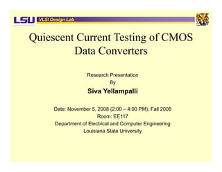
  • 1. VLSI Design Lab Quiescent Current Testing of CMOS Data Converters Research Presentation By Siva Yellampalli Date: November 5, 2008 (2:00 – 4:00 PM), Fall 2008 Room: EE117 Department of Electrical and Computer Engineering Louisiana State University
  • 2. VLSI Design Lab Outline of the Presentation IDDQ Testing methodology Testing data converter circuits Physical faults d fault injection technique Ph i l f lt and f lt i j ti t h i Future trends of IDDQ testing Circuit under test BICS for IDDQ testing BICS for ΔIDDQ testing Combined IDDQ, IDDT and oscillation test methodology methodology. IDDT current testing Oscillation based testing Conclusion C li
  • 3. VLSI Design Lab Outline of the Presentation IDDQ Testing Methodology Need for Testing Data Converter Circuits Physical Faults and Fault Injection Technique IDDQ BICS Design Future trends of IDDQ testing ΔIDDQ BICS Testing Combined IDDQ, IDDT and Oscillation Test Methodology IDDT Current Testing Oscillation Testing Conclusion
  • 4. VLSI Design Lab IDDQ Testing Methodology VDD VDD IDDQ=0 Q3 Q1 Vout V Vin Q2 Q4 With fault Without fault
  • 5. VLSI Design Lab Block Diagram of IDDQ Testing VDD PMOS BLOCK INPUTS OUTPUT NMOS BLOCK CUT PASS/FAIL BICS VSS
  • 6. VLSI Design Lab Need for Testing of Data Converter Circuits Photolithographic process Particle related defects have been observed as major cause of defects in mixed signal circuits. fd f t i i di l i it Physical failures -bridges -opens and -gate oxide shorts (GOS) gate (GOS).
  • 7. VLSI Design Lab Bridging Faults VDD Bridging faults -short circuit faults in integrated circuits. it t d i it -can appear either at the logical output of a g g p gate or at V0 the transistor nodes internal VA to a gate. Bridge 1: Drain-gate VB Bridge 3 : Drain-source Bridge 2 : Gate-source Gate source
  • 8. VLSI Design Lab Bridging Faults B id i F l Different bridging faults*: (a) shorting of seven metal lines caused by unexposed photo resist, (b) shorting of four metal lines by solid state particle on the metal mask, (c) shorts and breaks of metal lines caused by scratch in the photo resist, (d) short among multiple metal lines by a metallization defect of 1um in size, (e) short between two aluminum lines due to metallization defects, and (f) inter layer short between two aluminum interconnects in 0 5 um technology 0.5 technology. *R. Rajsuman, “IDDQ testing for CMOS VLSI,” Proc. of the IEEE, vol. 88, no. 4, 2000, pp. 544-566.
  • 9. VLSI Design Lab Gate Oxide Faults Gate oxide shorts -occur frequently in CMOS technology. -reasons are breakdown of the gate oxide and th manufacturing t id d the fti spot defects in lithography and processes on the active area and polysilicon masks masks. Gate Oxide defects: (a) gate- oxide short to N+ diffusion*, and (b) gate oxide pin hole causing cell word line leakage memory+ . *C.F. Hawkins and J.M. Soden, “Reliability and electrical properties of gate oxide shorts in CMOS ICs,” Proc. Int. Test Conf., 1986, pp. 443- 451. +A. Chan, D. Lam, W. Tan and S.Y. Khim, “Electrical failure analysis in high density DRAMs,” Proc. Int. Test Conf., 1998, pp. 43-52.
  • 10. VLSI Design Lab Open Faults (a) a foreign particle causing a line open and a ling thinning* (b) A contaminated particle causing 7- 7 line opens* and (c) SEM picture of defect which caused open in metal 2 and a short p in metal 1+. *W. Maly, “Realistic fault modeling for VLSI testing,” IEEE Design Auto. Conf., 1987, pp. 173-180. +J. Khare, S. Griep, H.D. Oberle, W.Maly, D.S. Landsiedel, U. Kollmer and D. M. H. Walker, “Key attributes of an SRAM testing strategy required for effective process monitoring,” IEEE Int. workshop on Memory Testing, 1993, pp. 84-89.
  • 11. VLSI Design Lab Fault Injection Technique Example: Fault-Injection Transistor (N- MOSFET) at Inverter Output VDD VE G ME VI V0 S D D (4.5/1.6) (4.5/1.6) ME VE G S FIT VSS
  • 12. VLSI Design Lab Outline of the Presentation IDDQ Testing methodology Need for Testing data converter circuits Physical faults d fault injection technique Ph i l f lt and f lt i j ti t h i IDDQBICS design Future trends of IDDQ testing g BICS for ΔIDDQ testing IPS current testing Oscillation based testing Conclusion
  • 13. VLSI Design Lab Outline of the Presentation IDDQ Testing Methodology Need for Testing Data Converter Circuits Physical Faults and Fault Injection Technique IDDQ BICS Design Future trends of IDDQ testing ΔIDDQ BICS Testing Combined IDDQ, IDDT and Oscillation Test Methodology IDDT Current Testing Oscillation Testing Conclusion
  • 14. VLSI Design Lab VDD(+2.5V) XFIT 3 M8 M5 VE3 XFIT6 XFIT 2 M7 VE6 VSS VSS VE2 VSS CMOS Amplifier (CUT) VOUT M1 M2 VE5 XFIT 5 V+ - V VBIAS M11 (XFIT8) VSS CC M10 XFIT 1 M6 VSS M3 M4 VE7 VE4 VE1 XFIT 7 XFIT 4 VSS(-2.5V) VDD BICS VDD 5.6/1.6 M5 11.6/1.6 M6 VDD VSS IDEF IREF EXT VSS 6.4/1.6 IDEF - IREF OUTPUT IREF 36/1.6 ( PASS/ FAIL ) M4 92/1.6 3.2/1.6 M1 M3 M2 M0 100/1.6 VENABLE 400/1.6 VSS 36/1.6 VSS(-2.5V)
  • 15. VLSI Design Lab Simulated Si l t d BICS O t t and M Output d Measured IDDQ f d for Defects
  • 16. VLSI Design Lab Layout of Built-in Current Sensor
  • 17. VLSI Design Lab BICS Showing PASS/FAIL Output from HP1660CS Logic Analyzer Corresponding to Fault M5DSS
  • 18. VLSI Design Lab Future Trends of IDDQ Testing The theoretical basis of IDDQ testing is based upon estimation of defect-free defect free current in the circuit and then setting a limit (threshold) above which a circuit is considered defective. Methods for tti threshold limit M th d f setting th h ld li it - 1μA is considered defect free any number from as low as 10 μA to 100 μA is considered as threshold limit. - Due to large number of devices, the distribution of the measured current is expected to be Guassian. Due to statistical variations IC’s up to mean +3σ are considered variations, IC s defect free. A limit higher than mean +3σ is assumed, above which IC’s are considered defective.
  • 19. VLSI Design Lab Future Trends of IDDQ Testing When the density of the defect free and defective current defect-free are separated from each other, clear distinction between the good and the defective ICs can be made. In submicron CMOS technology the mean of the distribution of defect free current increases and approaches the IDDQ threshold limit (set from earlier technology) Changing the threshold limit to higher number does not resolve the issue because with high leakage current the change in defect-free and defective current is miniscule and unidentifiable.
  • 20. VLSI Design Lab Future Trends of IDDQ Testing Sub threshold leakage current. ⎛ Vgs −Vth ⎞ ⎛ ⎛ Vds ⎞ ⎞ ⎜ ⎟⎜ ⎜ ⎜ v ⎟⎟ ⎜ S / ln10 ⎟ ⎟ = k exp⎝ ⎠ ⎜1 − exp⎝ t ⎠ ⎟ I sub ⎜ ⎟ ⎜ ⎟ ⎝ ⎠
  • 21. VLSI Design Lab Future Trends of IDDQ T ti Ft Tdf Testing Design Methods D i M th d - Reduced temperature - Substrate bias - Switched source impedance leakage reduction technique - Dual threshold method Testing methods - ΔIDDQ Testing - Power supply current testing - Oscillation testing method
  • 22. VLSI Design Lab Future Trends of IDDQ Testing ΔIDDQ Testing of CMOS ICs - relative methods of the offstate current is taken instead of absolute ones for fault detection. Power supply current based testing method. pp y g -variation of AC ripple in the supply current under the application of AC input stimulus is used for fault detection. Oscillation based t ti method. O ill ti b d testing th d - Converting the CUT is into an oscillator using feedback. - Output oscillation frequency is monitored for faults in the CUT. - Needs no test signal generation, uses simple measurement and has high fault coverage.
  • 23. VLSI Design Lab Outline of the Presentation IDDQ Testing methodology Testing data converter circuits Physical faults d fault injection technique Ph i l f lt and f lt i j ti t h i Future trends of IDDQ testing Circuit under test BICS for IDDQ testing BICS for ΔIDDQ testing IDDT current testing Oscillation based testing Conclusion
  • 24. VLSI Design Lab Outline of the Presentation IDDQ Testing Methodology Need for Testing Data Converter Circuits Physical Faults and Fault Injection Technique IDDQ BICS Design Future trends of IDDQ testing ΔIDDQ BICS Testing Combined IDDQ, IDDT and Oscillation Test Methodology IDDT Current Testing Oscillation Testing Conclusion
  • 25. VLSI Design Lab ∆IDDQ BICS Design and Testing VDD TG1 VTG Discharging input to comparator 4-Bit Binary Discharging Comp. Synchronous y Input to output 4-Bit Comp Counter Comparator pulse Output Output TG2 Count 1 Pulse A 1 B Analog g I/P Comp 0 C C CUT 0 D I DDQ CLK I/P Vref
  • 26. VLSI Design Lab Layout of BICS
  • 27. VLSI Design Lab Comparator Design VDD = 2.5V 3/0.6 3/0.6 M8 M10 M12 6.6/0.6 6.6/0.6 5.4/0.6 M3 M4 V OUT N2 N N1 Inv1 0.9/0.6 0 9/0 6 0.9/0.6 0 9/0 6 V NEG V POS M1 M2 30/0.6 30/0.6 M5 M6 M9 M11 M13 3.9/0.6 1.5/0.6 1.5/0.6 12/0.6 M7 GND
  • 28. VLSI Design Lab Analog-to-Digital Converter
  • 29. VLSI Design Lab Analog-to-Digital Converter
  • 30. VLSI Design Lab 3-BIT Flash Architecture ADC 2.5v 3 BIT 3-BIT flash architecture 1.5R based ADC. Designed for operation at R 2.5 2 5 V in 0 5 μm n well 0.5 n-well R CMOS technology. Output Digital The various blocks are word R N 2 -1 to N encoder - voltage reference R - resister ladder - seven comparators R - 8:3 encoder R 0.5R
  • 31. VLSI Design Lab 3-BIT Charge Scaling Architecture DAC Designed for operation at 2.5 V. VOUT Building Blocks: g 2pF 1pF 0.5pF p Reset R 0.5pF 05 F - Voltage Reference - Binary Switches - Scaling Network D2 D1 D0 -O Operational Amplifier ti l A lifi VReference
  • 32. VLSI Design Lab Low Voltage Operational Amplifier Design Double Ended Bulk Driving Second Biasing Differential to Single Ended High Swing Stage Circuitry Circuitry Input Stage Conversion Stage Circuitry (Class A Amplifier) VDD VON + VT M3 M17 M21 VON 2VON +VT M15 M4 M14 M19 M12 M23 VON +VT M11 M1 M2 Mb VPOS M6 VNEG M7 VOUT MR Cc M9 M5 M8 M22 M20 M10 M13 M16 M18 Note: For the P-MOSFETS the substrate is connected to VDD
  • 33. VLSI Design Lab Layout of Op-Amp
  • 34. VLSI Design Lab 12 bit 12-bit ADC with Induced Faults
  • 35. VLSI Design Lab Simulation of the Comparator With no Fault
  • 36. VLSI Design Lab Chip layout of 12 bit ADC in 40 pin 12-bit 40-pin Padframe
  • 37. VLSI Design Lab Microphotograph of Fabricated Chip Part of 12-bit ADC ΔIDDQ BICS
  • 38. VLSI Design Lab Experimental Results
  • 39. VLSI Design Lab Simulated Count Values from SPICE and Experimental Values for all the Five Faults
  • 40. VLSI Design Lab Equivalent Faults VDD FIT FIT M17 M19 R R OUTPUT INPUT FIT FIT M18 M20 R R VSS VSUBSTRATE Low Voltage op-amp.
  • 41. VLSI Design Lab Double Ended Bulk Driving Second Biasing Differential to Single Ended High Swing Stage Circuitry Circuitry Input Stage Conversion Stage Circuitry (Class A Amplifier) VDD VON + VT M3 M17 M21 VON 2VON +VT M15 M4 M14 M19 M12 M23 VON +VT M11 M1 M2 Mb VPOS M6 VNEG M7 VOUT MR Cc M9 M5 M8 M22 M20 M10 M13 M16 M18 Note: For the P-MOSFETS the substrate is connected to VDD
  • 42. VLSI Design Lab Scan Path Test
  • 43. VLSI Design Lab VCO Output ∆IDDQ BICS Design and Testing
  • 44. VLSI Design Lab Comparator Design
  • 45. VLSI Design Lab 12-bit Digital-to Analog Converter Unity Gain y Capacitor Array Architecture Storage TG Switch Buffer Unity Gain Capacitor OPAMP 64 c MSB Array LSB Array 63 Vo CH C C 2C 4C 8C 16C 32C C 2C 4C 8C 16C 32C Sample and Hold Input Circuitry To Generate Digital Input Word Output of Multiplexer VREF Control Signal
  • 46. VLSI Design Lab Layout of a 12 Bit DAC 12-Bit
  • 48. VLSI Design Lab Deviation (%) in Frequency Output of BICS Under Fault Injection Conditions
  • 49. VLSI Design Lab Outline of the Presentation IDDQ Testing methodology Testing data converter circuits Physical faults and fault injection technique Future trends of IDDQ testing Circuit under test BICS for IDDQ testing BICS for ΔIDDQ testing Combined IDDQ, IDDT and oscillation test methodology. methodology IDDT current testing Oscillation based testing Conclusion C li
  • 50. VLSI Design Lab Outline of the Presentation IDDQ Testing Methodology Need for Testing Data Converter Circuits Physical Faults and Fault Injection Technique IDDQ BICS Design Future trends of IDDQ testing ΔIDDQ BICS Testing Combined IDDQ, IDDT and Oscillation Test Methodology IDDT Current Testing Oscillation Testing Conclusion
  • 51. VLSI Design Lab Test methodology VDD CUT Input Functional Output Pass/Fail fOSC Additional BICS Feedback Circuitry
  • 52. VLSI Design Lab IDDT based testing methodology AC ripple in the p pp power supply current IDDT, passing pp y p g through VDD under the application of an AC input stimulus is measured. The i Th input signal should produce a noticeable amount of ti l h ld d ti bl tf difference between the IDDT of each faulty and fault-free cases hence a square wave is used. Tolerance limit for the magnitude of IDDT is set as ±5% such that it takes in account the deviations of significant technology and design parameters parameters. If the magnitude of IDDT with fault falls out of this tolerance range the fault is detected. g
  • 53. VLSI Design Lab IDDT based testing methodology A small resistor is used to sense th voltage corresponding the lt di VDD to IDDT. This resistor shows 100 Ω VR insignificant variation on CUT i i ifi t i ti CUTs performance. Input signal to the CUT is 4 V p g PMOS p-p, 5 kHz or 1 kHz square kH kH BLOCK wave. INPUT OUTPUT NMOS BLOCK CUT Block diagram of power supply current, IDDT based testing VSS
  • 54. VLSI Design Lab Two stage CMOS op-amp VDD(+2.5V) XFIT 3 M5 VE3 XFIT 2 XFIT 6 M7 M8 VE2 VE6 VSS VSS VSS VOUT VE5 XFIT 5 V+ V- M2 M1 VBIAS M11 CC VSS M6 VSS XFIT 1 M10 VE7 VE4 M4 VE1 M3 XFIT 7 XFIT 4 VSS(-2.5V)
  • 55. VLSI Design Lab Spice Simulated IPS for CUT 1
  • 56. VLSI Design Lab Measured IDDT (AC Ripple) for CUT1 ( pp ) For No Fault, Faults 4 and 6 are Input Voltage injected one at a time for CUT Input is a square wave 4 V p-p at 5 Voltage kHz. kHz Corresponding to IPS IDDT is 74 µA sensed across a 100Ω resistor
  • 57. VLSI Design Lab SPICE Si l t d and E p i nt l R lt f Simulated nd Experimental Results for CUT 1 IPS in µA IPS in µA Fault Number (Simulated) (Si l t d) (Experimental) (E i t l) No fault 74 74 Fault F lt 1 804 830 Fault 2 95 130 Fault 3 93 120 Fault 4 74 74 Fault 5 170 - Fault 6 73 74 Fault 7 156 268 Loss of IPS. +
  • 58. VLSI Design Lab Oscillation based test method Consists of converting the R1 R2 CUT into an oscillator using passive/ active components in the fOSC feedback. C R
  • 59. VLSI Design Lab Two stage CMOS op-amp VDD(+2.5V) XFIT 3 M5 VE3 XFIT 2 XFIT 6 M7 M8 VE2 VE6 VSS VSS VSS VOUT VE5 XFIT 5 V+ V- M2 M1 VBIAS M11 CC VSS M6 VSS XFIT 1 M10 VE7 VE4 M4 VE1 M3 XFIT 7 XFIT 4 VSS(-2.5V)
  • 60. VLSI Design Lab FFT Simulations for Evaluating the Oscillation Frequency of the CUT Oscillator 2 1 V o ltag e, (V ) 0 ( 1.5E-05 2.0E-05 2.5E-05 3.0E-05 3.5E-05 -1 -2 -3 T ime (s) The natural oscillation frequency (f NAT) was observed to be 875 kHz.
  • 61. VLSI Design Lab Monte-Carlo Analysis Nominal N i l range of oscillation f f ill ti frequencies i d t i is determined using M t i d i Monte- Carlo analysis by including the tolerance of components and parameters of the CUT. A device tolerance of 5% has been used for the frequency varying components R1, R2, R, C. Process variation effects on the electrical characteristics (viz., Vth, µ0 etc.) need to be considered while evaluating the fault tolerance. A lot tolerance 5% for Vth has been considered here. It can been simulated using SPICE command .MC |# runs| [Anal Type] |output variable| {list} {output | output specification}.
  • 62. VLSI Design Lab Tolerance band of Oscillation Frequencies With 5% tolerances for the components (R, C, R1, R2) and with 5% for Vth , the tolerance band of oscillation frequency was observed to be [-3.7%, +4.1%] and f MAX = 910 kHz f MIN = 842 kHz Note: The tolerance band is calculated as follows: [Min, Max] = [(f MIN- f NAT)/ f NAT, (f MAX- f NAT)/ f NAT]
  • 63. VLSI Design Lab Measured Oscillation Frequency
  • 64. VLSI Design Lab % Deviation from Natural frequency
  • 65. VLSI Design Lab Conclusion BICS for IDDQ t ti have been d i f testing h b designed f f lt d for fault detection. Circuits like op-amp, ADC and DAC have been designed op amp, as CUTs. Faults have been introduced using FITs. A new BICS for ΔIDDQ testing has been presented. Testing methods combining IDDQ, power supply current and oscillation current have been implemented implemented.
  • 66. VLSI Design Lab Thank Th k you