Nelamangala Call Girls: 🍓 7737669865 🍓 High Profile Model Escorts | Bangalore...
Ch05
1. PHYS 162 - Chapter 5 Transistor Bias Circuits
Prepared By: Syed Muhammad Asad – Semester 102 Page 1
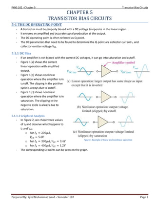
Figure 1 Example of linear and nonlinear operation
CHAPTER 5
TRANSISTOR BIAS CIRCUITS
5-1 THE DC OPERATING POINT
- A transistor must be properly biased with a DC voltage to operate in the linear region.
- It ensures an amplified and accurate signal production at the output.
- The DC operating point is often referred as Q-point.
- The DC parameters that need to be found to determine the Q-point are collector current IC and
collector-emitter voltage VCE.
5.1.1 DC Bias
- If an amplifier is not biased with the correct DC voltages, it can go into saturation and cutoff.
- Figure 1(a) shows the correct
linear operation with amplified
output.
- Figure 1(b) shows nonlinear
operation where the amplifier is in
cutoff. The clipping in the positive
cycle is always due to cutoff.
- Figure 1(c) shows nonlinear
operation where the amplifier is in
saturation. The clipping in the
negative cycle is always due to
saturation.
5.1.1.1 Graphical Analysis
- In Figure 2, we chose three values
of IB and observe what happens to
IC and VCE.
o For 𝐼 𝐵 = 200𝜇𝐴,
𝑉𝐶𝐸 = 5.6𝑉
o For 𝐼 𝐵 = 300𝜇𝐴, 𝑉𝐶𝐸 = 3.4𝑉
o For 𝐼 𝐵 = 400𝜇𝐴, 𝑉𝐶𝐸 = 1.2𝑉
- The corresponding Q-points can be seen on the graph.
2. PHYS 162 - Chapter 5 Transistor Bias Circuits
Prepared By: Syed Muhammad Asad – Semester 102 Page 2
5.1.1.2 DC Load Line
- The DC operation of a transistor circuit can be described graphically using a DC load line.
- It is a straight line connecting 𝐼 𝐶 = 𝐼 𝐶 𝑠𝑎𝑡 on the y-axis to 𝑉𝐶𝐸 = 𝑉𝐶𝐶 on the x-axis.
- At saturation 𝐼 𝐶 𝑠𝑎𝑡 =
𝑉 𝐶𝐶 −𝑉 𝐶𝐸 𝑠𝑎𝑡
𝑅 𝐶
and at cutoff 𝑉𝐶𝐸 = 𝑉𝐶𝐶.
- Figure 3 shows the three Q-points.
Figure 2 Q-point adjustment
Figure 3 The Dc load line
3. PHYS 162 - Chapter 5 Transistor Bias Circuits
Prepared By: Syed Muhammad Asad – Semester 102 Page 3
5.1.1.3 Linear Operation
- All point along the DC load line between saturation and cutoff is the linear region of operation for a
transistor.
- Figure 4 is an example of linear operation.
- AC voltage Vin produces an AC base current 𝐼𝑏(𝑝𝑒𝑎𝑘 ) = 100𝜇𝐴 above and below the Q-point.
- This produces an AC collector current 𝐼𝑐(𝑝𝑒𝑎𝑘 ) = 10𝑚𝐴 above and below the Q-point.
- This change in the collector current changes the collector-emitter voltage 𝑉𝑐𝑒(𝑝𝑒𝑎𝑘 ) = 2.2𝑉.
- This changing Vce is the required voltage amplification at the output of the transistor.
NOTE: REFER EXAMPLE 5-1 PAGE 221
5-2 VOLTAGE-DIVIDER BIAS
- Voltage-divider bias is one of the widely used biasing techniques for a
transistor.
- It uses a single power source and a voltage-divider to attain the voltage
base bias voltage.
- For circuit analysis, it is assumed that the base current IB is small enough
to be neglected.
- There are two types of voltage-dividers.
o Stiff voltage divider where
𝑉𝐵 =
𝑅2
𝑅1 + 𝑅2
𝑉𝐶𝐶
If 𝑅𝐼𝑁 𝐵𝐴𝑆𝐸 ≥ 10𝑅2
o Non Stiff voltage divider where
𝑉𝐵 =
𝑅2||𝑅𝐼𝑁 𝐵𝐴𝑆𝐸
𝑅1 + 𝑅2||𝑅𝐼𝑁 𝐵𝐴𝑆𝐸
𝑉𝐶𝐶
If 𝑅𝐼𝑁 𝐵𝐴𝑆𝐸 < 10𝑅2
- 𝑅𝐼𝑁 𝐵𝐴𝑆𝐸 = 𝛽 𝐷𝐶 𝑅 𝐸
Figure 4 Variation in AC current and voltage
Figure 5 Voltage-divider bias
4. PHYS 162 - Chapter 5 Transistor Bias Circuits
Prepared By: Syed Muhammad Asad – Semester 102 Page 4
NOTE: REFER EXAMPLE 5-2 PAGE 224
5-3 OTHER BIAS METHODS
- Other types of biasing methods are
o Emitter Bias
Excellent Q-point stability.
Uses two voltages sources instead of one.
o Base Bias
Mainly used for switching circuits.
Not suitable for linear amplifier because of poor Q-point stability.
o Emitter-Feedback Bias
Adding an RE in Base bias circuits gives emitter-feedback bias.
Better Q-point stability than the base bias but still not well enough for linear operation.
o Collector-Feedback Bias
Better Q-point stability than emitter-feedback bias.
Can be used in linear amplifier circuits.
- A summary of all the equations is given in Table 1.
Table 1 Transistor Bias Circuit Formula Sheet
Voltage-Divider Bias Emitter Bias Base Bias Emitter-Feedback
Bias
Collector-
Feedback Bias
Stiff voltage-divider
𝑉𝐵 =
𝑅2
𝑅1 + 𝑅2
𝑉𝐶𝐶
If 𝑅𝐼𝑁 𝐵𝐴𝑆𝐸 ≥ 10𝑅2
Non Stiff voltage divider
𝑉𝐵 =
𝑅2||𝑅𝐼𝑁 𝐵𝐴𝑆𝐸
𝑅1 + 𝑅2||𝑅𝐼𝑁 𝐵𝐴𝑆𝐸
𝑉𝐶𝐶
If 𝑅𝐼𝑁 𝐵𝐴𝑆𝐸 < 10𝑅2
𝑉𝐵 = 𝑉𝐸 + 𝑉𝐵𝐸
𝑅𝐼𝑁 𝐵𝐴𝑆𝐸 = 𝛽 𝐷𝐶 𝑅 𝐸
𝑉𝐸 = 𝑉𝐵 − 𝑉𝐵𝐸 𝑉𝐸 ≈ −1𝑉 (neglecting
effect of 𝛽 𝐷𝐶 )
𝑉𝐸 = 𝑉𝐸𝐸 + 𝐼 𝐸 𝑅 𝐸(taking
𝛽 𝐷𝐶 into account)
𝐼 𝐶 ≅ 𝐼 𝐸 =
𝑉𝐸
𝑅 𝐸
Without 𝛽 𝐷𝐶
𝐼 𝐶 ≅ 𝐼 𝐸 =
−𝑉𝐸𝐸 − 1𝑉
𝑅 𝐸
With 𝛽 𝐷𝐶
𝐼 𝐶 ≅ 𝐼 𝐸 =
−𝑉𝐸𝐸 − 𝑉𝐵𝐸
𝑅 𝐸 + 𝑅 𝐵/𝛽 𝐷𝐶
𝐼 𝐶 = 𝛽 𝐷𝐶
𝑉𝐶𝐶 − 𝑉𝐵𝐸
𝑅 𝐵
𝐼 𝐶 ≅ 𝐼 𝐸 =
𝑉𝐶𝐶 − 𝑉𝐵𝐸
𝑅 𝐸 + 𝑅 𝐵/𝛽 𝐷𝐶
𝐼 𝐶 =
𝑉𝐶𝐶 − 𝑉𝐵𝐸
𝑅 𝐶 + 𝑅 𝐵/𝛽 𝐷𝐶
𝑉𝐶 = 𝑉𝐶𝐶 − 𝐼 𝐶 𝑅 𝐶 𝑉𝐶 = 𝑉𝐶𝐶 − 𝐼 𝐶 𝑅 𝐶
𝑉𝐶𝐸 = 𝑉𝐶 − 𝑉𝐸 𝑉𝐶𝐸 = 𝑉𝐶 − 𝑉𝐸 𝑉𝐶𝐸 = 𝑉𝐶𝐶 − 𝐼 𝐶 𝑅 𝐶 𝑉𝐶𝐸 = 𝑉𝐶𝐶 − 𝐼 𝐶 𝑅 𝐶 + 𝑅 𝐸 𝑉𝐶𝐸 = 𝑉𝐶𝐶 − 𝐼 𝐶 𝑅 𝐶
NOTE: REFER EXAMPLE 5-6, 5-7, 5-8, 5-9, 5-10 PAGE 230-236