SlideShare ist ein Scribd-Unternehmen logo
1 von 53
Downloaden Sie, um offline zu lesen
UNIT-IV: TIME-BASE GENERATORS
(Part- 2 PPT)
• Transistor constant current sweep circuit
• Current Time-Base Generators: A Simple Current
Sweep, Linearity Correction through Adjustment of
Driving Waveform, Transistor Current Time-Base
generator.
Mr. M. Balaji, Dept. of ECE, SVEC 1
Transistor constant current sweep circuit
• The sweep voltage generated by an exponential sweep generator is
non-linear as the current in the capacitor varies exponentially.
• However, to generate a linear sweep, the capacitor is required to
charge with a constant current.
• As discussed in the earlier concepts, the collector current in the CE
configuration may not remain constant with the variation in VCE.
• However, from the output characteristics of the CB configuration,
we see that for a constant value of IE, IC is independent of VCB and
the curves are parallel to the VCB axis, except for a small range of
values of VCB.
Mr. M. Balaji, Dept. of ECE, SVEC 2
Mr. M. Balaji, Dept. of ECE, SVEC 3
• In the output characteristics of a CB configuration, IC remains
practically constant with the variation in VCB, except, at
smaller values of VCB.
• This suggests that if a capacitor is charged using the constant
collector current of the CB configuration, the resultant
sweep voltage must be a linear sweep voltage.
• Fig. 12.7(a) shows the circuit of a transistor constant current
sweep generator using the CB configuration. From Fig.
12.7(a),
• the current IE in the base loop is:
Mr. M. Balaji, Dept. of ECE, SVEC 4
Mr. M. Balaji, Dept. of ECE, SVEC 5
• Let the switch S be open at t = 0.
• The collector current is constant and is given by the relation:
IC = hFBIE
Hence, C charges with the constant IC and the voltage across the capacitor
varies linearly as a function of time.
To determine the sweep voltage Vs, let us consider the small signal model of
the transistor in the CB configuration as shown in Fig. 12.7(b)
Mr. M. Balaji, Dept. of ECE, SVEC 6
--- (1)
--- (2)
--- (3)
Mr. M. Balaji, Dept. of ECE, SVEC 7
--- (4)
--- (5)
--- (6)
From equation (1), we get
, In equation 3, we get
Mr. M. Balaji, Dept. of ECE, SVEC 8
Mr. M. Balaji, Dept. of ECE, SVEC 9
Mr. M. Balaji, Dept. of ECE, SVEC 10
--- (7)
Mr. M. Balaji, Dept. of ECE, SVEC 11
Equation (7) reduces to
Mr. M. Balaji, Dept. of ECE, SVEC 12
Mr. M. Balaji, Dept. of ECE, SVEC 13
• As the second term in the bracket tends to be small, es is small.
• The constant current sweep generator shown in Fig. 12.7(a) is modified
such that a single source VYY is used to derive VEE and VCC sources, as
shown in Fig.12.8.
Mr. M. Balaji, Dept. of ECE, SVEC 14
• In Fig. 12.8, D1 and D2 are Zener diodes.
• VEE is derived from the VYY source using these diodes such that
VEE = (VZ1 + VZ2)
where VZ1 and VZ2 are the breakdown voltages of D1 and D2.
Similarly, the VCC source is also derived using the VYY source (the
Zener current through R derives VCC).
Hence, a single voltage source is used in the circuit shown in Fig.
12.8 when compared to the circuit shown in Fig. 12.7(a). RL is the
load connected.
Mr. M. Balaji, Dept. of ECE, SVEC 15
Mr. M. Balaji, Dept. of ECE, SVEC 16
Mr. M. Balaji, Dept. of ECE, SVEC 17
Mr. M. Balaji, Dept. of ECE, SVEC 18
Mr. M. Balaji, Dept. of ECE, SVEC 19
Principle of current time base generator
• When a constant current is made to flow through a capacitor C, voltage across capacitor would
be a voltage time base waveform
𝑉𝑐 𝑡 =
1
𝐶
න 𝑖 𝑡 𝑑𝑡
=
𝐼
𝐶
𝑡
where I/C is the slope of the voltage time base waveform.
• The dual of the above statement about current time base waveform is “ the current iL(t) flowing
through an inductor L would become a time base waveform if we maintain a constant voltage V
across an inductor.
𝐼𝐿 𝑡 =
1
𝐿
න 𝑉 𝑡 𝑑𝑡
=
𝑉
𝐿
𝑡
where V/L is the slope of the current time base waveform.
Mr. M. Balaji, Dept. of ECE, SVEC 20
A simple current time base circuit
• The basic principle employed in current sweep generators is
electromagnetic deflection.
• In these sweep generators, when a voltage is applied to a coil of inductance
L, the current in the inductance increases linearly with time.
• A simple current sweep generator is shown in Fig. 13.1(a).
• The circuit basically consists of a transistor used as a switch driven by a
trigger signal.
• The current in the inductor rises exponentially during the period the switch
is closed (the transistor is ON).
• At the end of the trigger signal, the device switches into the OFF state and
the current in the inductor decays.
Mr. M. Balaji, Dept. of ECE, SVEC 21
Mr. M. Balaji, Dept. of ECE, SVEC 22
• At t< 0, Q is in cut off, so VCE= VCC; IL= 0;
• At t = 0; Q is in saturation, VCE = VCE(sat) ; so Diode D is reverse biased,
therefore iL flows through L
iL =
1
𝐿
‫׬‬ 𝑉𝐶𝐶 𝑑𝑡 =
𝑉 𝐶𝐶
𝐿
t
At t= Ts, Q is in cut off; diode D conducts, iL flows through Rd
at collector Vcc+ iL Rd develops. iL continues to flow through the diode D and
resistor Rd until it exponentially decays to zero.
The time constant of this exponential decay is τ = L/ Rd, where Rd is the sum
of damping resistance and diode forward resistance
𝑖 𝐿 𝑡 > 𝑇𝑠 = 𝑖 𝐿 𝑒
−
𝑅 𝑑
𝐿
𝑡
Mr. M. Balaji, Dept. of ECE, SVEC 23
Mr. M. Balaji, Dept. of ECE, SVEC 24
• When the inductor is fully charged at infinity, the current flowing through it
is only limited by the yoke resistance RL and collector saturation resistance
of transistor Rcs. Then
I=
𝑉𝑐𝑐
𝑅 𝐿+𝑅 𝑐𝑠
Generalized transient equation of an inductor is
𝑖 𝐿 𝑡 = 𝑖 𝐿 ∞ + 𝑖 𝐿(0) − 𝑖 𝐿(∞) 𝑒− 𝑅 𝐿+𝑅 𝑐𝑠 𝑡/𝐿
=
𝑉𝑐𝑐
𝑅 𝐿+𝑅 𝑐𝑠
+ 0 −
𝑉𝑐𝑐
𝑅 𝐿+𝑅 𝑐𝑠
𝑒− 𝑅 𝐿+𝑅 𝑐𝑠 𝑡/𝐿
=
𝑉𝑐𝑐
𝑅 𝐿+𝑅 𝑐𝑠
[1 - 𝑒− 𝑅 𝐿+𝑅 𝑐𝑠 𝑡/𝐿]
Expanding the exponential into series
Mr. M. Balaji, Dept. of ECE, SVEC 25
=
𝑉𝑐𝑐
𝑅 𝐿+𝑅 𝑐𝑠
1 − (1 +
−(𝑅 𝐿+𝑅 𝑐𝑠)𝑡
𝐿
+
(𝑅 𝐿+𝑅 𝑐𝑠)2 𝑡2
2𝐿2 )
=
𝑉𝑐𝑐
𝑅 𝐿+𝑅 𝑐𝑠
(𝑅 𝐿+𝑅 𝑐𝑠)𝑡
𝐿
1 −
(𝑅 𝐿+𝑅 𝑐𝑠)𝑡
2𝐿
=
𝑉 𝐶𝐶 𝑡
𝐿
1 −
(𝑅 𝐿+𝑅 𝑐𝑠)𝑡
2𝐿
:. iL(t)=
𝑉 𝐶𝐶 𝑡
𝐿
neglect second term and iL will be iLmax when t= Ts
iL(t)=
𝑉 𝐶𝐶 𝑇 𝑠
𝐿
Mr. M. Balaji, Dept. of ECE, SVEC 26
Slope error es
𝑒𝑠 =
ቚ
𝑑𝑖 𝐿
𝑑𝑡 𝑡
=
0
−
ቚ
𝑑𝑖 𝐿
𝑑𝑡 𝑡
=
𝑇𝑠
ቚ
𝑑𝑖 𝐿
𝑑𝑡 𝑡
=
0
iL =
𝑉𝑐𝑐 𝑡
𝑅 𝐿+𝑅 𝑐𝑠
[1 - 𝑒− 𝑅 𝐿+𝑅 𝑐𝑠 𝑡/𝐿
]
𝑑𝑖 𝐿
𝑑𝑡
=
𝑉 𝐶𝐶
𝐿
(1- 𝑒− 𝑅 𝐿+𝑅 𝑐𝑠 𝑡/𝐿
)
ቚ
𝑑𝑖 𝐿
𝑑𝑡 𝑡 = 0 =
𝑉 𝐶𝐶
𝐿
Mr. M. Balaji, Dept. of ECE, SVEC 27
ቚ
𝑑𝑖 𝐿
𝑑𝑡 𝑡 = 0 =
𝑉 𝐶𝐶
𝐿
(1- 𝑒− 𝑅 𝐿+𝑅 𝑐𝑠 𝑇𝑠/𝐿
)
𝑒𝑠 =
ቚ
𝑑𝑖 𝐿
𝑑𝑡 𝑡
=
0
−
ቚ
𝑑𝑖 𝐿
𝑑𝑡 𝑡
=
𝑇𝑠
ቚ
𝑑𝑖 𝐿
𝑑𝑡 𝑡
=
0
es =
𝑅 𝐿+𝑅 𝑐𝑠 𝑇𝑠
𝐿
Mr. M. Balaji, Dept. of ECE, SVEC 28
we know iL =
𝑉 𝐶𝐶 𝑇 𝑆
𝐿
𝑇𝑠
𝐿
=
𝑖 𝐿
𝑉 𝐶𝐶
:. es =
(𝑅 𝐿+𝑅 𝑐𝑠)𝑖 𝐿
𝑉 𝐶𝐶
to maintain linearity, iL (𝑅 𝐿 + 𝑅 𝑐𝑠) ≪ 𝑉𝐶𝐶
Mr. M. Balaji, Dept. of ECE, SVEC 29
Linearity Correction through Adjustment of Driving Waveform
The non-linearity encountered in the previous circuit is:
as the inductor (yoke) current increases, the current in the internal resistance
of the source Rs also increases. Consequently the voltage across the inductor
decreases (as shown in Figure below).
Mr. M. Balaji, Dept. of ECE, SVEC 30
So, vL = Vs − iLRs as vs is constant at Vs.
If we can compensate for the voltage developed across the resistance Rs then
the current sweep tends to be linear.
This can be achieved as shown in figure below.
Mr. M. Balaji, Dept. of ECE, SVEC 31
-
Let Rs be the internal resistance of the source vs.
The total circuit resistance is (Rs + RL ).
Now, if we want the inductor current to vary linearly, i.e., iL = Kt
(where K is the constant of proportionality) then the source voltage vs is,
Mr. M. Balaji, Dept. of ECE, SVEC 32
This waveform consists of a step followed by a ramp (Rs+RL)Kt. Such
a waveform is called a trapezoidal waveform.
We can thus see that if the driving signal is trapezoidal as given by Equation
above, then the current sweep is linear (i.e., iL = Kt).
The Norton representation of the driving source, using Eq.(13.3) is:
Mr. M. Balaji, Dept. of ECE, SVEC 33
The waveform of this current source is also a step followed by a ramp (as
shown in Figure in next slide). Thus, a trapezoidal driving waveform
generates a linear current sweep.
At the end of the sweep, the current once again will return to zero
exponentially with a time constant τ = L/(Rs + RL).
Generally, Rs >> RL, hence, τ ≈ L/Rs.
Mr. M. Balaji, Dept. of ECE, SVEC 34
The question now is, should Rs be small or should it be large?
The resistance Rs is chosen based on two conflicting requirements.
If Rs is small, the current will decay slowly and a long period will
have to elapse before another sweep is possible, i.e., the fly-back
time becomes unacceptably long. This could be construed as a
disadvantage.
However, the advantage is that the peak voltage developed across
the inductor (= ILRs) may not be unduly large.
As a result, the voltage at the collector of the transistor when the
sweep terminates (= VCC + ILRs), which reverse-biases the base-
collector diode of the transistor may not be large enough to
damage the device.
Mr. M. Balaji, Dept. of ECE, SVEC 35
Alternately, if Rs is large, the current will decay rapidly.
This means that the retrace time is negligible, which
enables us to initiate the next sweep immediately after the
sweep duration.
For this, Rs is required to be large. However, a large peak
voltage will appear across the inductor and the voltage that
now reverse-biases the base-emitter diode of the transistor
may be excessively large and can damage the device.
Mr. M. Balaji, Dept. of ECE, SVEC 36
Generally, a compromise has to be struck such that the spike
amplitude is not appreciably large and also the inductor current
decays in a smaller time interval.
Normally, to achieve this, a damping resistance Rd is connected
across the yoke to limit the peak voltage.
Let R be the parallel combination of Rs and Rd .
Then the retrace time constant is τr = L/R.
The trapezoidal waveform required to improve the linearity of the
current sweep is generated using the circuit shown in next slide,
we have:
Mr. M. Balaji, Dept. of ECE, SVEC 37
Mr. M. Balaji, Dept. of ECE, SVEC 38
Vo = V – I R2
Mr. M. Balaji, Dept. of ECE, SVEC 39
Expanding the exponential as a series and limiting to the first few terms
of the expansion, we have:
Thus, the first term is a step and the second term represents a ramp.
Therefore, vo is a step followed by ramp (trapezoidal).
Mr. M. Balaji, Dept. of ECE, SVEC 40
Transistor Current Time-Base generator
Mr. M. Balaji, Dept. of ECE, SVEC 41
Mr. M. Balaji, Dept. of ECE, SVEC 42
Mr. M. Balaji, Dept. of ECE, SVEC 43
Mr. M. Balaji, Dept. of ECE, SVEC 44
Mr. M. Balaji, Dept. of ECE, SVEC 45
Mr. M. Balaji, Dept. of ECE, SVEC 46
Here, Q1 acts as switch which serves the function of S, it is ON when the
input is zero and is OFF when the input goes negative.
R1, R2 and C1 generate the trapezoidal driving waveform.
Q2 and Q3 combination is a Darlington pair and RE stabilizes iL.
The Darlington emitter follower provides a large input resistance and thus
eliminates the loading on the driving source by its input.
The current iL varies linearly with time.
Mr. M. Balaji, Dept. of ECE, SVEC 47
Mr. M. Balaji, Dept. of ECE, SVEC 48
When the transistor is in saturation, the entire voltage Vcc will appear
across the inductor. If the current reaches the maximum value IL max in
time Ts, then
Mr. M. Balaji, Dept. of ECE, SVEC 49
Mr. M. Balaji, Dept. of ECE, SVEC 50
Mr. M. Balaji, Dept. of ECE, SVEC 51
Mr. M. Balaji, Dept. of ECE, SVEC 52
Mr. M. Balaji, Dept. of ECE, SVEC 53

Weitere ähnliche Inhalte

Was ist angesagt?

Was ist angesagt? (20)

Differentiator OP Amp
Differentiator OP AmpDifferentiator OP Amp
Differentiator OP Amp
 
Field effect transistors
Field effect transistorsField effect transistors
Field effect transistors
 
Basics of amplifier.ppt
Basics of amplifier.pptBasics of amplifier.ppt
Basics of amplifier.ppt
 
amplifier
amplifieramplifier
amplifier
 
Lecture Notes: EEEC6440315 Communication Systems - Inter Symbol Interference...
Lecture Notes:  EEEC6440315 Communication Systems - Inter Symbol Interference...Lecture Notes:  EEEC6440315 Communication Systems - Inter Symbol Interference...
Lecture Notes: EEEC6440315 Communication Systems - Inter Symbol Interference...
 
Frequency response(1)
Frequency response(1)Frequency response(1)
Frequency response(1)
 
Silicon control rectifier
Silicon control rectifierSilicon control rectifier
Silicon control rectifier
 
Oscillators
OscillatorsOscillators
Oscillators
 
Adaptive equalization
Adaptive equalizationAdaptive equalization
Adaptive equalization
 
Tuned amplifiers
Tuned amplifiersTuned amplifiers
Tuned amplifiers
 
Analog to Digital Converter
Analog to Digital ConverterAnalog to Digital Converter
Analog to Digital Converter
 
Origin of biopotentials
Origin of biopotentialsOrigin of biopotentials
Origin of biopotentials
 
Amplifiers Pesentation
Amplifiers PesentationAmplifiers Pesentation
Amplifiers Pesentation
 
Eca unit 2
Eca unit 2Eca unit 2
Eca unit 2
 
Pre emphasis and de-emphasis
Pre emphasis and de-emphasisPre emphasis and de-emphasis
Pre emphasis and de-emphasis
 
Oscillators
OscillatorsOscillators
Oscillators
 
Analog modulation
Analog modulationAnalog modulation
Analog modulation
 
Instrumental lecture 2
Instrumental lecture 2Instrumental lecture 2
Instrumental lecture 2
 
555 timer vibrators
555 timer vibrators555 timer vibrators
555 timer vibrators
 
ANALOG TO DIGITAL CONVERTOR
ANALOG TO DIGITAL CONVERTORANALOG TO DIGITAL CONVERTOR
ANALOG TO DIGITAL CONVERTOR
 

Ähnlich wie Time Base Generators (part-2)

Short notes on digital electronics for specialist officer it exam by das sir,...
Short notes on digital electronics for specialist officer it exam by das sir,...Short notes on digital electronics for specialist officer it exam by das sir,...
Short notes on digital electronics for specialist officer it exam by das sir,...Tamal Kumar Das
 
Time base Generators (part-1)
Time base Generators (part-1)Time base Generators (part-1)
Time base Generators (part-1)m balaji
 
high-pass RC circuit.pptx
high-pass RC circuit.pptxhigh-pass RC circuit.pptx
high-pass RC circuit.pptxDeepthy Gs
 
Highpass RC circuit
Highpass RC circuitHighpass RC circuit
Highpass RC circuitm balaji
 
Kirchhoff's rules and rc circuits
Kirchhoff's rules and rc circuitsKirchhoff's rules and rc circuits
Kirchhoff's rules and rc circuitsramamaii
 
Time Domain response of second order linear circuit
Time Domain response of second order linear circuitTime Domain response of second order linear circuit
Time Domain response of second order linear circuitAbhishek Choksi
 
Phase Shift, Collpitt's and Crystal oscillators.pptx
Phase Shift, Collpitt's and Crystal oscillators.pptxPhase Shift, Collpitt's and Crystal oscillators.pptx
Phase Shift, Collpitt's and Crystal oscillators.pptxProfVilasShamraoPati
 
Phase Shift, Collpitt's and Crystal oscillators.pptx
Phase Shift, Collpitt's and Crystal oscillators.pptxPhase Shift, Collpitt's and Crystal oscillators.pptx
Phase Shift, Collpitt's and Crystal oscillators.pptxProfVilasShamraoPati
 
Comparative Steady State Analysis of Boost and Cascaded Boost Converter with ...
Comparative Steady State Analysis of Boost and Cascaded Boost Converter with ...Comparative Steady State Analysis of Boost and Cascaded Boost Converter with ...
Comparative Steady State Analysis of Boost and Cascaded Boost Converter with ...IAES-IJPEDS
 
Report on sawtooth wave generator
Report on sawtooth wave generatorReport on sawtooth wave generator
Report on sawtooth wave generatorAmit kumar
 
Zero voltage switching resonant power conversion
Zero voltage switching resonant power conversionZero voltage switching resonant power conversion
Zero voltage switching resonant power conversionPham Hoang
 
Transistors & Oscillators by Er. Swapnil Kaware
Transistors & Oscillators by Er. Swapnil KawareTransistors & Oscillators by Er. Swapnil Kaware
Transistors & Oscillators by Er. Swapnil KawareProf. Swapnil V. Kaware
 
Electronics and modern physics presentation
Electronics and modern physics presentationElectronics and modern physics presentation
Electronics and modern physics presentationNoorulainRazzaq
 
Bipolar junction transistor characterstics biassing and amplification, lab 9
Bipolar junction transistor characterstics biassing and amplification, lab 9Bipolar junction transistor characterstics biassing and amplification, lab 9
Bipolar junction transistor characterstics biassing and amplification, lab 9kehali Haileselassie
 
Chapter 10.ppt Large signal transfer circuits
Chapter 10.ppt Large signal transfer circuitsChapter 10.ppt Large signal transfer circuits
Chapter 10.ppt Large signal transfer circuitscbcbgdfgsdf
 

Ähnlich wie Time Base Generators (part-2) (20)

Short notes on digital electronics for specialist officer it exam by das sir,...
Short notes on digital electronics for specialist officer it exam by das sir,...Short notes on digital electronics for specialist officer it exam by das sir,...
Short notes on digital electronics for specialist officer it exam by das sir,...
 
Time base Generators (part-1)
Time base Generators (part-1)Time base Generators (part-1)
Time base Generators (part-1)
 
high-pass RC circuit.pptx
high-pass RC circuit.pptxhigh-pass RC circuit.pptx
high-pass RC circuit.pptx
 
Highpass RC circuit
Highpass RC circuitHighpass RC circuit
Highpass RC circuit
 
Kirchhoff's rules and rc circuits
Kirchhoff's rules and rc circuitsKirchhoff's rules and rc circuits
Kirchhoff's rules and rc circuits
 
Time Domain response of second order linear circuit
Time Domain response of second order linear circuitTime Domain response of second order linear circuit
Time Domain response of second order linear circuit
 
Phase Shift, Collpitt's and Crystal oscillators.pptx
Phase Shift, Collpitt's and Crystal oscillators.pptxPhase Shift, Collpitt's and Crystal oscillators.pptx
Phase Shift, Collpitt's and Crystal oscillators.pptx
 
Phase Shift, Collpitt's and Crystal oscillators.pptx
Phase Shift, Collpitt's and Crystal oscillators.pptxPhase Shift, Collpitt's and Crystal oscillators.pptx
Phase Shift, Collpitt's and Crystal oscillators.pptx
 
Electrical Device and Circuit
Electrical Device and CircuitElectrical Device and Circuit
Electrical Device and Circuit
 
Comparative Steady State Analysis of Boost and Cascaded Boost Converter with ...
Comparative Steady State Analysis of Boost and Cascaded Boost Converter with ...Comparative Steady State Analysis of Boost and Cascaded Boost Converter with ...
Comparative Steady State Analysis of Boost and Cascaded Boost Converter with ...
 
Report on sawtooth wave generator
Report on sawtooth wave generatorReport on sawtooth wave generator
Report on sawtooth wave generator
 
Zero voltage switching resonant power conversion
Zero voltage switching resonant power conversionZero voltage switching resonant power conversion
Zero voltage switching resonant power conversion
 
Transistors & Oscillators by Er. Swapnil Kaware
Transistors & Oscillators by Er. Swapnil KawareTransistors & Oscillators by Er. Swapnil Kaware
Transistors & Oscillators by Er. Swapnil Kaware
 
PP+for+Ch+31.pdf
PP+for+Ch+31.pdfPP+for+Ch+31.pdf
PP+for+Ch+31.pdf
 
Electronics and modern physics presentation
Electronics and modern physics presentationElectronics and modern physics presentation
Electronics and modern physics presentation
 
Sepic
SepicSepic
Sepic
 
3661.pdf
3661.pdf3661.pdf
3661.pdf
 
Bipolar junction transistor characterstics biassing and amplification, lab 9
Bipolar junction transistor characterstics biassing and amplification, lab 9Bipolar junction transistor characterstics biassing and amplification, lab 9
Bipolar junction transistor characterstics biassing and amplification, lab 9
 
Bipolar junction transistor characterstics biassing and amplification, lab 9
Bipolar junction transistor characterstics biassing and amplification, lab 9Bipolar junction transistor characterstics biassing and amplification, lab 9
Bipolar junction transistor characterstics biassing and amplification, lab 9
 
Chapter 10.ppt Large signal transfer circuits
Chapter 10.ppt Large signal transfer circuitsChapter 10.ppt Large signal transfer circuits
Chapter 10.ppt Large signal transfer circuits
 

Kürzlich hochgeladen

Intro To Electric Vehicles PDF Notes.pdf
Intro To Electric Vehicles PDF Notes.pdfIntro To Electric Vehicles PDF Notes.pdf
Intro To Electric Vehicles PDF Notes.pdfrs7054576148
 
Call Girls Wakad Call Me 7737669865 Budget Friendly No Advance Booking
Call Girls Wakad Call Me 7737669865 Budget Friendly No Advance BookingCall Girls Wakad Call Me 7737669865 Budget Friendly No Advance Booking
Call Girls Wakad Call Me 7737669865 Budget Friendly No Advance Bookingroncy bisnoi
 
notes on Evolution Of Analytic Scalability.ppt
notes on Evolution Of Analytic Scalability.pptnotes on Evolution Of Analytic Scalability.ppt
notes on Evolution Of Analytic Scalability.pptMsecMca
 
Thermal Engineering -unit - III & IV.ppt
Thermal Engineering -unit - III & IV.pptThermal Engineering -unit - III & IV.ppt
Thermal Engineering -unit - III & IV.pptDineshKumar4165
 
Thermal Engineering-R & A / C - unit - V
Thermal Engineering-R & A / C - unit - VThermal Engineering-R & A / C - unit - V
Thermal Engineering-R & A / C - unit - VDineshKumar4165
 
Navigating Complexity: The Role of Trusted Partners and VIAS3D in Dassault Sy...
Navigating Complexity: The Role of Trusted Partners and VIAS3D in Dassault Sy...Navigating Complexity: The Role of Trusted Partners and VIAS3D in Dassault Sy...
Navigating Complexity: The Role of Trusted Partners and VIAS3D in Dassault Sy...Arindam Chakraborty, Ph.D., P.E. (CA, TX)
 
VIP Call Girls Palanpur 7001035870 Whatsapp Number, 24/07 Booking
VIP Call Girls Palanpur 7001035870 Whatsapp Number, 24/07 BookingVIP Call Girls Palanpur 7001035870 Whatsapp Number, 24/07 Booking
VIP Call Girls Palanpur 7001035870 Whatsapp Number, 24/07 Bookingdharasingh5698
 
Double Revolving field theory-how the rotor develops torque
Double Revolving field theory-how the rotor develops torqueDouble Revolving field theory-how the rotor develops torque
Double Revolving field theory-how the rotor develops torqueBhangaleSonal
 
University management System project report..pdf
University management System project report..pdfUniversity management System project report..pdf
University management System project report..pdfKamal Acharya
 
KubeKraft presentation @CloudNativeHooghly
KubeKraft presentation @CloudNativeHooghlyKubeKraft presentation @CloudNativeHooghly
KubeKraft presentation @CloudNativeHooghlysanyuktamishra911
 
Top Rated Pune Call Girls Budhwar Peth ⟟ 6297143586 ⟟ Call Me For Genuine Se...
Top Rated  Pune Call Girls Budhwar Peth ⟟ 6297143586 ⟟ Call Me For Genuine Se...Top Rated  Pune Call Girls Budhwar Peth ⟟ 6297143586 ⟟ Call Me For Genuine Se...
Top Rated Pune Call Girls Budhwar Peth ⟟ 6297143586 ⟟ Call Me For Genuine Se...Call Girls in Nagpur High Profile
 
Unit 1 - Soil Classification and Compaction.pdf
Unit 1 - Soil Classification and Compaction.pdfUnit 1 - Soil Classification and Compaction.pdf
Unit 1 - Soil Classification and Compaction.pdfRagavanV2
 

Kürzlich hochgeladen (20)

Intro To Electric Vehicles PDF Notes.pdf
Intro To Electric Vehicles PDF Notes.pdfIntro To Electric Vehicles PDF Notes.pdf
Intro To Electric Vehicles PDF Notes.pdf
 
Call Girls Wakad Call Me 7737669865 Budget Friendly No Advance Booking
Call Girls Wakad Call Me 7737669865 Budget Friendly No Advance BookingCall Girls Wakad Call Me 7737669865 Budget Friendly No Advance Booking
Call Girls Wakad Call Me 7737669865 Budget Friendly No Advance Booking
 
notes on Evolution Of Analytic Scalability.ppt
notes on Evolution Of Analytic Scalability.pptnotes on Evolution Of Analytic Scalability.ppt
notes on Evolution Of Analytic Scalability.ppt
 
FEA Based Level 3 Assessment of Deformed Tanks with Fluid Induced Loads
FEA Based Level 3 Assessment of Deformed Tanks with Fluid Induced LoadsFEA Based Level 3 Assessment of Deformed Tanks with Fluid Induced Loads
FEA Based Level 3 Assessment of Deformed Tanks with Fluid Induced Loads
 
Call Girls in Ramesh Nagar Delhi 💯 Call Us 🔝9953056974 🔝 Escort Service
Call Girls in Ramesh Nagar Delhi 💯 Call Us 🔝9953056974 🔝 Escort ServiceCall Girls in Ramesh Nagar Delhi 💯 Call Us 🔝9953056974 🔝 Escort Service
Call Girls in Ramesh Nagar Delhi 💯 Call Us 🔝9953056974 🔝 Escort Service
 
Thermal Engineering -unit - III & IV.ppt
Thermal Engineering -unit - III & IV.pptThermal Engineering -unit - III & IV.ppt
Thermal Engineering -unit - III & IV.ppt
 
Thermal Engineering-R & A / C - unit - V
Thermal Engineering-R & A / C - unit - VThermal Engineering-R & A / C - unit - V
Thermal Engineering-R & A / C - unit - V
 
Navigating Complexity: The Role of Trusted Partners and VIAS3D in Dassault Sy...
Navigating Complexity: The Role of Trusted Partners and VIAS3D in Dassault Sy...Navigating Complexity: The Role of Trusted Partners and VIAS3D in Dassault Sy...
Navigating Complexity: The Role of Trusted Partners and VIAS3D in Dassault Sy...
 
VIP Call Girls Palanpur 7001035870 Whatsapp Number, 24/07 Booking
VIP Call Girls Palanpur 7001035870 Whatsapp Number, 24/07 BookingVIP Call Girls Palanpur 7001035870 Whatsapp Number, 24/07 Booking
VIP Call Girls Palanpur 7001035870 Whatsapp Number, 24/07 Booking
 
(INDIRA) Call Girl Meerut Call Now 8617697112 Meerut Escorts 24x7
(INDIRA) Call Girl Meerut Call Now 8617697112 Meerut Escorts 24x7(INDIRA) Call Girl Meerut Call Now 8617697112 Meerut Escorts 24x7
(INDIRA) Call Girl Meerut Call Now 8617697112 Meerut Escorts 24x7
 
(INDIRA) Call Girl Aurangabad Call Now 8617697112 Aurangabad Escorts 24x7
(INDIRA) Call Girl Aurangabad Call Now 8617697112 Aurangabad Escorts 24x7(INDIRA) Call Girl Aurangabad Call Now 8617697112 Aurangabad Escorts 24x7
(INDIRA) Call Girl Aurangabad Call Now 8617697112 Aurangabad Escorts 24x7
 
NFPA 5000 2024 standard .
NFPA 5000 2024 standard                                  .NFPA 5000 2024 standard                                  .
NFPA 5000 2024 standard .
 
Cara Menggugurkan Sperma Yang Masuk Rahim Biyar Tidak Hamil
Cara Menggugurkan Sperma Yang Masuk Rahim Biyar Tidak HamilCara Menggugurkan Sperma Yang Masuk Rahim Biyar Tidak Hamil
Cara Menggugurkan Sperma Yang Masuk Rahim Biyar Tidak Hamil
 
Call Girls in Netaji Nagar, Delhi 💯 Call Us 🔝9953056974 🔝 Escort Service
Call Girls in Netaji Nagar, Delhi 💯 Call Us 🔝9953056974 🔝 Escort ServiceCall Girls in Netaji Nagar, Delhi 💯 Call Us 🔝9953056974 🔝 Escort Service
Call Girls in Netaji Nagar, Delhi 💯 Call Us 🔝9953056974 🔝 Escort Service
 
Double Revolving field theory-how the rotor develops torque
Double Revolving field theory-how the rotor develops torqueDouble Revolving field theory-how the rotor develops torque
Double Revolving field theory-how the rotor develops torque
 
University management System project report..pdf
University management System project report..pdfUniversity management System project report..pdf
University management System project report..pdf
 
KubeKraft presentation @CloudNativeHooghly
KubeKraft presentation @CloudNativeHooghlyKubeKraft presentation @CloudNativeHooghly
KubeKraft presentation @CloudNativeHooghly
 
Top Rated Pune Call Girls Budhwar Peth ⟟ 6297143586 ⟟ Call Me For Genuine Se...
Top Rated  Pune Call Girls Budhwar Peth ⟟ 6297143586 ⟟ Call Me For Genuine Se...Top Rated  Pune Call Girls Budhwar Peth ⟟ 6297143586 ⟟ Call Me For Genuine Se...
Top Rated Pune Call Girls Budhwar Peth ⟟ 6297143586 ⟟ Call Me For Genuine Se...
 
Unit 1 - Soil Classification and Compaction.pdf
Unit 1 - Soil Classification and Compaction.pdfUnit 1 - Soil Classification and Compaction.pdf
Unit 1 - Soil Classification and Compaction.pdf
 
Water Industry Process Automation & Control Monthly - April 2024
Water Industry Process Automation & Control Monthly - April 2024Water Industry Process Automation & Control Monthly - April 2024
Water Industry Process Automation & Control Monthly - April 2024
 

Time Base Generators (part-2)

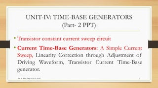
  • 1. UNIT-IV: TIME-BASE GENERATORS (Part- 2 PPT) • Transistor constant current sweep circuit • Current Time-Base Generators: A Simple Current Sweep, Linearity Correction through Adjustment of Driving Waveform, Transistor Current Time-Base generator. Mr. M. Balaji, Dept. of ECE, SVEC 1
  • 2. Transistor constant current sweep circuit • The sweep voltage generated by an exponential sweep generator is non-linear as the current in the capacitor varies exponentially. • However, to generate a linear sweep, the capacitor is required to charge with a constant current. • As discussed in the earlier concepts, the collector current in the CE configuration may not remain constant with the variation in VCE. • However, from the output characteristics of the CB configuration, we see that for a constant value of IE, IC is independent of VCB and the curves are parallel to the VCB axis, except for a small range of values of VCB. Mr. M. Balaji, Dept. of ECE, SVEC 2
  • 3. Mr. M. Balaji, Dept. of ECE, SVEC 3
  • 4. • In the output characteristics of a CB configuration, IC remains practically constant with the variation in VCB, except, at smaller values of VCB. • This suggests that if a capacitor is charged using the constant collector current of the CB configuration, the resultant sweep voltage must be a linear sweep voltage. • Fig. 12.7(a) shows the circuit of a transistor constant current sweep generator using the CB configuration. From Fig. 12.7(a), • the current IE in the base loop is: Mr. M. Balaji, Dept. of ECE, SVEC 4
  • 5. Mr. M. Balaji, Dept. of ECE, SVEC 5
  • 6. • Let the switch S be open at t = 0. • The collector current is constant and is given by the relation: IC = hFBIE Hence, C charges with the constant IC and the voltage across the capacitor varies linearly as a function of time. To determine the sweep voltage Vs, let us consider the small signal model of the transistor in the CB configuration as shown in Fig. 12.7(b) Mr. M. Balaji, Dept. of ECE, SVEC 6
  • 7. --- (1) --- (2) --- (3) Mr. M. Balaji, Dept. of ECE, SVEC 7
  • 8. --- (4) --- (5) --- (6) From equation (1), we get , In equation 3, we get Mr. M. Balaji, Dept. of ECE, SVEC 8
  • 9. Mr. M. Balaji, Dept. of ECE, SVEC 9
  • 10. Mr. M. Balaji, Dept. of ECE, SVEC 10
  • 11. --- (7) Mr. M. Balaji, Dept. of ECE, SVEC 11
  • 12. Equation (7) reduces to Mr. M. Balaji, Dept. of ECE, SVEC 12
  • 13. Mr. M. Balaji, Dept. of ECE, SVEC 13
  • 14. • As the second term in the bracket tends to be small, es is small. • The constant current sweep generator shown in Fig. 12.7(a) is modified such that a single source VYY is used to derive VEE and VCC sources, as shown in Fig.12.8. Mr. M. Balaji, Dept. of ECE, SVEC 14
  • 15. • In Fig. 12.8, D1 and D2 are Zener diodes. • VEE is derived from the VYY source using these diodes such that VEE = (VZ1 + VZ2) where VZ1 and VZ2 are the breakdown voltages of D1 and D2. Similarly, the VCC source is also derived using the VYY source (the Zener current through R derives VCC). Hence, a single voltage source is used in the circuit shown in Fig. 12.8 when compared to the circuit shown in Fig. 12.7(a). RL is the load connected. Mr. M. Balaji, Dept. of ECE, SVEC 15
  • 16. Mr. M. Balaji, Dept. of ECE, SVEC 16
  • 17. Mr. M. Balaji, Dept. of ECE, SVEC 17
  • 18. Mr. M. Balaji, Dept. of ECE, SVEC 18
  • 19. Mr. M. Balaji, Dept. of ECE, SVEC 19
  • 20. Principle of current time base generator • When a constant current is made to flow through a capacitor C, voltage across capacitor would be a voltage time base waveform 𝑉𝑐 𝑡 = 1 𝐶 න 𝑖 𝑡 𝑑𝑡 = 𝐼 𝐶 𝑡 where I/C is the slope of the voltage time base waveform. • The dual of the above statement about current time base waveform is “ the current iL(t) flowing through an inductor L would become a time base waveform if we maintain a constant voltage V across an inductor. 𝐼𝐿 𝑡 = 1 𝐿 න 𝑉 𝑡 𝑑𝑡 = 𝑉 𝐿 𝑡 where V/L is the slope of the current time base waveform. Mr. M. Balaji, Dept. of ECE, SVEC 20
  • 21. A simple current time base circuit • The basic principle employed in current sweep generators is electromagnetic deflection. • In these sweep generators, when a voltage is applied to a coil of inductance L, the current in the inductance increases linearly with time. • A simple current sweep generator is shown in Fig. 13.1(a). • The circuit basically consists of a transistor used as a switch driven by a trigger signal. • The current in the inductor rises exponentially during the period the switch is closed (the transistor is ON). • At the end of the trigger signal, the device switches into the OFF state and the current in the inductor decays. Mr. M. Balaji, Dept. of ECE, SVEC 21
  • 22. Mr. M. Balaji, Dept. of ECE, SVEC 22
  • 23. • At t< 0, Q is in cut off, so VCE= VCC; IL= 0; • At t = 0; Q is in saturation, VCE = VCE(sat) ; so Diode D is reverse biased, therefore iL flows through L iL = 1 𝐿 ‫׬‬ 𝑉𝐶𝐶 𝑑𝑡 = 𝑉 𝐶𝐶 𝐿 t At t= Ts, Q is in cut off; diode D conducts, iL flows through Rd at collector Vcc+ iL Rd develops. iL continues to flow through the diode D and resistor Rd until it exponentially decays to zero. The time constant of this exponential decay is τ = L/ Rd, where Rd is the sum of damping resistance and diode forward resistance 𝑖 𝐿 𝑡 > 𝑇𝑠 = 𝑖 𝐿 𝑒 − 𝑅 𝑑 𝐿 𝑡 Mr. M. Balaji, Dept. of ECE, SVEC 23
  • 24. Mr. M. Balaji, Dept. of ECE, SVEC 24
  • 25. • When the inductor is fully charged at infinity, the current flowing through it is only limited by the yoke resistance RL and collector saturation resistance of transistor Rcs. Then I= 𝑉𝑐𝑐 𝑅 𝐿+𝑅 𝑐𝑠 Generalized transient equation of an inductor is 𝑖 𝐿 𝑡 = 𝑖 𝐿 ∞ + 𝑖 𝐿(0) − 𝑖 𝐿(∞) 𝑒− 𝑅 𝐿+𝑅 𝑐𝑠 𝑡/𝐿 = 𝑉𝑐𝑐 𝑅 𝐿+𝑅 𝑐𝑠 + 0 − 𝑉𝑐𝑐 𝑅 𝐿+𝑅 𝑐𝑠 𝑒− 𝑅 𝐿+𝑅 𝑐𝑠 𝑡/𝐿 = 𝑉𝑐𝑐 𝑅 𝐿+𝑅 𝑐𝑠 [1 - 𝑒− 𝑅 𝐿+𝑅 𝑐𝑠 𝑡/𝐿] Expanding the exponential into series Mr. M. Balaji, Dept. of ECE, SVEC 25
  • 26. = 𝑉𝑐𝑐 𝑅 𝐿+𝑅 𝑐𝑠 1 − (1 + −(𝑅 𝐿+𝑅 𝑐𝑠)𝑡 𝐿 + (𝑅 𝐿+𝑅 𝑐𝑠)2 𝑡2 2𝐿2 ) = 𝑉𝑐𝑐 𝑅 𝐿+𝑅 𝑐𝑠 (𝑅 𝐿+𝑅 𝑐𝑠)𝑡 𝐿 1 − (𝑅 𝐿+𝑅 𝑐𝑠)𝑡 2𝐿 = 𝑉 𝐶𝐶 𝑡 𝐿 1 − (𝑅 𝐿+𝑅 𝑐𝑠)𝑡 2𝐿 :. iL(t)= 𝑉 𝐶𝐶 𝑡 𝐿 neglect second term and iL will be iLmax when t= Ts iL(t)= 𝑉 𝐶𝐶 𝑇 𝑠 𝐿 Mr. M. Balaji, Dept. of ECE, SVEC 26
  • 27. Slope error es 𝑒𝑠 = ቚ 𝑑𝑖 𝐿 𝑑𝑡 𝑡 = 0 − ቚ 𝑑𝑖 𝐿 𝑑𝑡 𝑡 = 𝑇𝑠 ቚ 𝑑𝑖 𝐿 𝑑𝑡 𝑡 = 0 iL = 𝑉𝑐𝑐 𝑡 𝑅 𝐿+𝑅 𝑐𝑠 [1 - 𝑒− 𝑅 𝐿+𝑅 𝑐𝑠 𝑡/𝐿 ] 𝑑𝑖 𝐿 𝑑𝑡 = 𝑉 𝐶𝐶 𝐿 (1- 𝑒− 𝑅 𝐿+𝑅 𝑐𝑠 𝑡/𝐿 ) ቚ 𝑑𝑖 𝐿 𝑑𝑡 𝑡 = 0 = 𝑉 𝐶𝐶 𝐿 Mr. M. Balaji, Dept. of ECE, SVEC 27
  • 28. ቚ 𝑑𝑖 𝐿 𝑑𝑡 𝑡 = 0 = 𝑉 𝐶𝐶 𝐿 (1- 𝑒− 𝑅 𝐿+𝑅 𝑐𝑠 𝑇𝑠/𝐿 ) 𝑒𝑠 = ቚ 𝑑𝑖 𝐿 𝑑𝑡 𝑡 = 0 − ቚ 𝑑𝑖 𝐿 𝑑𝑡 𝑡 = 𝑇𝑠 ቚ 𝑑𝑖 𝐿 𝑑𝑡 𝑡 = 0 es = 𝑅 𝐿+𝑅 𝑐𝑠 𝑇𝑠 𝐿 Mr. M. Balaji, Dept. of ECE, SVEC 28
  • 29. we know iL = 𝑉 𝐶𝐶 𝑇 𝑆 𝐿 𝑇𝑠 𝐿 = 𝑖 𝐿 𝑉 𝐶𝐶 :. es = (𝑅 𝐿+𝑅 𝑐𝑠)𝑖 𝐿 𝑉 𝐶𝐶 to maintain linearity, iL (𝑅 𝐿 + 𝑅 𝑐𝑠) ≪ 𝑉𝐶𝐶 Mr. M. Balaji, Dept. of ECE, SVEC 29
  • 30. Linearity Correction through Adjustment of Driving Waveform The non-linearity encountered in the previous circuit is: as the inductor (yoke) current increases, the current in the internal resistance of the source Rs also increases. Consequently the voltage across the inductor decreases (as shown in Figure below). Mr. M. Balaji, Dept. of ECE, SVEC 30
  • 31. So, vL = Vs − iLRs as vs is constant at Vs. If we can compensate for the voltage developed across the resistance Rs then the current sweep tends to be linear. This can be achieved as shown in figure below. Mr. M. Balaji, Dept. of ECE, SVEC 31 -
  • 32. Let Rs be the internal resistance of the source vs. The total circuit resistance is (Rs + RL ). Now, if we want the inductor current to vary linearly, i.e., iL = Kt (where K is the constant of proportionality) then the source voltage vs is, Mr. M. Balaji, Dept. of ECE, SVEC 32 This waveform consists of a step followed by a ramp (Rs+RL)Kt. Such a waveform is called a trapezoidal waveform.
  • 33. We can thus see that if the driving signal is trapezoidal as given by Equation above, then the current sweep is linear (i.e., iL = Kt). The Norton representation of the driving source, using Eq.(13.3) is: Mr. M. Balaji, Dept. of ECE, SVEC 33 The waveform of this current source is also a step followed by a ramp (as shown in Figure in next slide). Thus, a trapezoidal driving waveform generates a linear current sweep. At the end of the sweep, the current once again will return to zero exponentially with a time constant τ = L/(Rs + RL). Generally, Rs >> RL, hence, τ ≈ L/Rs.
  • 34. Mr. M. Balaji, Dept. of ECE, SVEC 34
  • 35. The question now is, should Rs be small or should it be large? The resistance Rs is chosen based on two conflicting requirements. If Rs is small, the current will decay slowly and a long period will have to elapse before another sweep is possible, i.e., the fly-back time becomes unacceptably long. This could be construed as a disadvantage. However, the advantage is that the peak voltage developed across the inductor (= ILRs) may not be unduly large. As a result, the voltage at the collector of the transistor when the sweep terminates (= VCC + ILRs), which reverse-biases the base- collector diode of the transistor may not be large enough to damage the device. Mr. M. Balaji, Dept. of ECE, SVEC 35
  • 36. Alternately, if Rs is large, the current will decay rapidly. This means that the retrace time is negligible, which enables us to initiate the next sweep immediately after the sweep duration. For this, Rs is required to be large. However, a large peak voltage will appear across the inductor and the voltage that now reverse-biases the base-emitter diode of the transistor may be excessively large and can damage the device. Mr. M. Balaji, Dept. of ECE, SVEC 36
  • 37. Generally, a compromise has to be struck such that the spike amplitude is not appreciably large and also the inductor current decays in a smaller time interval. Normally, to achieve this, a damping resistance Rd is connected across the yoke to limit the peak voltage. Let R be the parallel combination of Rs and Rd . Then the retrace time constant is τr = L/R. The trapezoidal waveform required to improve the linearity of the current sweep is generated using the circuit shown in next slide, we have: Mr. M. Balaji, Dept. of ECE, SVEC 37
  • 38. Mr. M. Balaji, Dept. of ECE, SVEC 38 Vo = V – I R2
  • 39. Mr. M. Balaji, Dept. of ECE, SVEC 39 Expanding the exponential as a series and limiting to the first few terms of the expansion, we have:
  • 40. Thus, the first term is a step and the second term represents a ramp. Therefore, vo is a step followed by ramp (trapezoidal). Mr. M. Balaji, Dept. of ECE, SVEC 40
  • 41. Transistor Current Time-Base generator Mr. M. Balaji, Dept. of ECE, SVEC 41
  • 42. Mr. M. Balaji, Dept. of ECE, SVEC 42
  • 43. Mr. M. Balaji, Dept. of ECE, SVEC 43
  • 44. Mr. M. Balaji, Dept. of ECE, SVEC 44
  • 45. Mr. M. Balaji, Dept. of ECE, SVEC 45
  • 46. Mr. M. Balaji, Dept. of ECE, SVEC 46
  • 47. Here, Q1 acts as switch which serves the function of S, it is ON when the input is zero and is OFF when the input goes negative. R1, R2 and C1 generate the trapezoidal driving waveform. Q2 and Q3 combination is a Darlington pair and RE stabilizes iL. The Darlington emitter follower provides a large input resistance and thus eliminates the loading on the driving source by its input. The current iL varies linearly with time. Mr. M. Balaji, Dept. of ECE, SVEC 47
  • 48. Mr. M. Balaji, Dept. of ECE, SVEC 48 When the transistor is in saturation, the entire voltage Vcc will appear across the inductor. If the current reaches the maximum value IL max in time Ts, then
  • 49. Mr. M. Balaji, Dept. of ECE, SVEC 49
  • 50. Mr. M. Balaji, Dept. of ECE, SVEC 50
  • 51. Mr. M. Balaji, Dept. of ECE, SVEC 51
  • 52. Mr. M. Balaji, Dept. of ECE, SVEC 52
  • 53. Mr. M. Balaji, Dept. of ECE, SVEC 53