SlideShare ist ein Scribd-Unternehmen logo
1 von 7
Downloaden Sie, um offline zu lesen
Lecture Notes in Microelectronics
Torsten Lehmann
October 14, 2008
1 MOS design equations
S
B
D
G
−
+
D
B
S
G +
vGS
−
+
−
vBS
vDS
+
−
+
−
vGS
iDS
vDS
+
iDS
−
vBS
(B)(A)
Figure 1: MOS transistor symbol, voltage and current definitions; (A) NMOS transistor
(B) PMOS transistor.
NMOS PMOS
full symbol
bulk implicit
switch
depletion
high-voltage
Figure 2: MOS transistor varieties.
1
1.1 Support equations
threshold voltage Vth = Vth0 + γ |2φF − vBS| − |2φF| (1)
n/p sign function |x|p ≡
x for n-channel
−x for p-channel
; |x|p =
γ
|γ|
x (2)
sub-threshold slope n =
γ
2 |2φF − vBS|
+ |1|p (3)
gate-overdrive voltage vEff = vGS − Vth (4)
velocity saturation µ =
µ0
1 + vDS/(ECritL)
(5)
drain saturation voltage vDSsat = LECrit 1 + 2vEff/(LECrit) − 1 (6)
≃ vEff, |2vEff|p ≪ |LECrit|p (7)
drain current factor β =
W
L
K′
=
W
L
µCox; K′
= µCox (8)
channel-length modulation α = 1 + λvDS = 1 +
kλvDS
L
; λ =
kλ
L
(9)
thermal voltage VT = kT/q (10)
sub-threshold scale current I0 = 1
2
µCox(2nVT )2
(11)
weak-strong transition IWST = I0 ln2
(2)
W
L
(12)
1.2 Current equations
Strong inversion (|vEff|p >∼ |2nVT ln(10)|p, or |IDS,sat|p ≫ |IWST|p):
iDS = µCox
W
L
vEffvDS − 1
2
v2
DS α, |vDSsat|p > |vDS|p (triode) (13)
iDS = IDS,sat = µCox
W
L
vEffvDSsat − 1
2
v2
DSsat α, |vDSsat|p ≤ |vDS|p (saturation)(14)
≃ 1
2
µCox
W
L
v2
Effα, |2vEff|p ≪ |LECrit|p (not velocity saturated) (15)
≃ µ0CoxECritW vEff − 1
2
vDSsat α, |2vEff|p ≫ |LECrit|p (deep velocity sat.) (16)
Weak inversion (|vEff|p <∼ −|2nVT ln(10)|p, or |IDS,sat|p ≪ |IWST|p):
iDS = I0
W
L
evEff /(nVT )
1 − e−|vDS|p/VT
α (17)
iDS = IDS,sat = I0
W
L
evEff /(nVT )
α, |nVT |p ≪ |vDS|p (saturation) (18)
Moderate inversion saturation (|vDS|p ≫ |nVT |p, and |vDS|p > |vEff|p):
iDS = IDS,sat = 1
2
µCox
W
L
(2nVT )2
ln2
1 + evEff /(2nVT )
α (19)
2
0.001
0.01
0.1
1
10
100
1000
-4 -2 0 2 4
iDS/Iwst
veff/nVT
current expression
(log(1+exp(x/2))/log(2))**2
x**2/(log(2)*2)**2
exp(x)/log(2)**2
Figure 3: Normalised saturation current
1.3 Sample MOST parameters
Typical parameters for some CMOS processes (preliminary):
Process 0.35 µm 0.18 µm
Parameter n-channel p-channel n-channel p-channel
VDD,max 2.5 V 2.5 V 1.8 V 1.8 V
Vth0 0.6 V −0.6 V 0.5 V −0.5 V
γ 0.5
√
V −0.5
√
V 0.6
√
V −0.4
√
V
2φF 0.7 V −0.7 V 0.8 V −0.8 V
n (zero bias) 1.3 −1.3 1.4 −1.3
Lmin 0.35 µm 0.35 µm 0.18 µm 0.18 µm
kλ 0.1 µm/V −0.1 µm/V 0.12 µm/V −0.08 µm/V
µ0Cox 120 µA/V2
−40 µA/V2
260 µA/V2
−65 µA/V2
Cox 4 fF/µm2
4 fF/µm2
8 fF/µm2
8 fF/µm2
Cj0 0.8 fF/µm2
1.2 fF/µm2
2 fF/µm2
2 fF/µm2
Cj0sw 0.3 fF/µm 0.4 fF/µm 0.6 fF/µm 0.6 fF/µm
Cov 0.2 fF/µm 0.2 fF/µm 0.1 fF/µm 0.1 fF/µm
xj 0.1 µm 0.1 µm 0.05 µm 0.05 µm
ℓsd 1 µm 1 µm 0.5 µm 0.5 µm
λ (DRC) 0.2 µm 0.2 µm 0.1 µm 0.1 µm
ECrit ∞ −∞ 2.2 V/µm −5 V/µm
3
2 Noise
Calculating total input referred noise is often impossible, as the integral typically diverges
for both high frequencies (white noise) and low frequencies (1/f noise). The total output
referred noise is easier, as any circuit has an upper band-width — typically, this doesn’t
solve the 1/f divergence problem, however. My suggestion is to equate the lower frequency
bound to 1/Tobs, where Tobs is the observation time of the system (e.g., the time it is turned
on — say a day or so):
V 2
no,tot =
∞
1/Tobs i
V 2
ni(f)|Hi(f)|2
df
3 Matching
To a first order approximation, the relative variance of drain current in MOS transistor
biased in strong inversion saturation can be expressed as:
σ2
D
I2
D
=
BW
LW2
+
BL
WL2
+
BK
WL(µCox)2
+ 4
BV
WL(VGS − Vth)2
(20)
where ID is the average (nominal) drain current, and the Bs are constants. For relatively
large transistors and a given gate bias voltage, this simplifies to:
σ2
D
I2
D
≃
BI
WL
(21)
4
4 Problems
4.1 Problem 1
vOUT
vIN
IB
VDD
VSS
Figure 4: Common source amplifier
The common source amplifier in figure 4 is biased with a DC drain current of IB = 1 µA.
It is to be implemented in the 0.35 µm process, where the smallest transistor dimensions
allowed (for this amplifier) is 0.7 µm.
• Find W and L such that the transistor is biased in weak inversion. Find for this
transistor all the small-signal parameters (gm, rds, Cgs, Cgd, Csb, and Cdb) and the
low-frequency voltage gain, Av. Find also fT for the transistor.
• Now find W and L such that the transistor is biased in strong inversion, and again
find gm, rds, Av and fT. For this amplifier, what must the DC bias value, VIN, of in
the input voltage be? What must VIN be if the source voltage is 1 V rather than 0 V
as on the figure?
• Finally, find W and L such that the transistor is biased in strong inversion, but has
the same gate area as the weak-inversion amplifier, and find gm, rds, Av and fT.
4.2 Problem 2
For the circuit in figure 5, prove that
i1 − i2 = µCox
W
L
v1v2 ,
when all transistors are identical and operate in the triode region (the bulk affect can be
ignored).
4.3 Problem 3
For the CMOS nand-gate in figure 6, find all transistors widths, W and lengths, L such
that the gate can drive a load capacitance of CL = 1 pF in less than 5 ns.
5
0V by feedbackv2
v1
i1
i2
Figure 5: Cross-coupled transistor pairs
z
a
b
CL
N
N
PP
DDV
(a)
param N P unit
µCox 92 −30 µA/V2
Vth 0.8 −0.9 V
Lmin 0.8 µm
VDD 2 V
(b)
Figure 6: Static CMOS nand-gate (a) and circuit and transistor parameters (b)
4.4 Problem 4
a
b
z
CL
VB
SN
SN
N
P
DDV
Figure 7: CSL nand-gate
For the Current Steering Logic (CSL) nand-gate in figure 7, find all transistors widths,
W and lengths, L, and the bias voltage, VB such that the gate can drive a load capacitance
of CL = 1 pF in less than 5 ns; use the same circuit and transistor parameters as in problem
3.
6
4.5 Problem 5
word line
bit line
MS
MC
VB
(a)
param val unit
Cox 5 fF/µm2
Lmin 0.35 µm
Cj(sb, sd) 1.5 fF · W
VDD 3 V
(b)
Figure 8: DRAM cell (a) and transistor parameters
The dynamic RAM cell in figure 8 is arranged in a square, 1 cm2
matrix. Estimate the
largest number of bits in the matrix when the sense amplifier can detect a 50 mV voltage
difference and relevant transistor parameters are given in the figure. Transistor ms is a
switch transistor while transistor MC act as a storage capacitor. The bias voltage, VB is
chosen > VDD + Vth, and the word-line is like-wise clock-boosted to a voltage > VDD + Vth
when high. Find also the widths, W and lengths, L for the transistors.
4.6 Problem 6
iin iout
Figure 9: Current mirror
For a given vGS, the relative drain current variation (in saturation) is given by
σ2
I2
D
=
BI
WL
, BI = 5 · 10−4
µm2
,
where ID is the average drain current and σ2
is the variance of the drain current. The
drain current is assumed to be normally distributed. For the current mirror in figure 9
with W/L = 5µm/2µm for both transistors, what is the probability that |iout − iin| < 1 %?
4.7 Problem 7
A wafer has a defect density of D = 0.01 cm−2
. Chips on the wafer are 2 cm2
in size,
each having 1000 sub-components that perform outside specifications with a probability of
0.002 % each. Find the fraction of chips which function within specifications after manu-
facturing.
7

Weitere ähnliche Inhalte

Was ist angesagt?

The Revolution from Transistor to Digital Electronics
The Revolution from Transistor to Digital ElectronicsThe Revolution from Transistor to Digital Electronics
The Revolution from Transistor to Digital ElectronicsSubhajit Bhattacharjee
 
Ixan0010 drivers igbt
Ixan0010 drivers igbtIxan0010 drivers igbt
Ixan0010 drivers igbtDario Delgado
 
Pass Transistor Logic
Pass Transistor LogicPass Transistor Logic
Pass Transistor LogicDiwaker Pant
 
Lec4 Intro to Computer Engineering by Hsien-Hsin Sean Lee Georgia Tech -- CMOS
Lec4 Intro to Computer Engineering by Hsien-Hsin Sean Lee Georgia Tech -- CMOSLec4 Intro to Computer Engineering by Hsien-Hsin Sean Lee Georgia Tech -- CMOS
Lec4 Intro to Computer Engineering by Hsien-Hsin Sean Lee Georgia Tech -- CMOSHsien-Hsin Sean Lee, Ph.D.
 
Original N-Channel Power MOSFET IRF1010EPBF IRF1010 1010 60V 84A TO-220 New I...
Original N-Channel Power MOSFET IRF1010EPBF IRF1010 1010 60V 84A TO-220 New I...Original N-Channel Power MOSFET IRF1010EPBF IRF1010 1010 60V 84A TO-220 New I...
Original N-Channel Power MOSFET IRF1010EPBF IRF1010 1010 60V 84A TO-220 New I...AUTHELECTRONIC
 
B1 b3 b2_row_b20_b28a_and_b28b_tx_load_pull_matching_tuning
B1 b3 b2_row_b20_b28a_and_b28b_tx_load_pull_matching_tuningB1 b3 b2_row_b20_b28a_and_b28b_tx_load_pull_matching_tuning
B1 b3 b2_row_b20_b28a_and_b28b_tx_load_pull_matching_tuningPei-Che Chang
 
CMOS logic circuits
CMOS logic circuitsCMOS logic circuits
CMOS logic circuitsMahesh_Naidu
 
Colpitts startup
Colpitts startupColpitts startup
Colpitts startupvulanskyi
 
Lecture11 combinational logic dynamics
Lecture11 combinational logic dynamicsLecture11 combinational logic dynamics
Lecture11 combinational logic dynamicsvidhya DS
 
Multiband Transceivers - [Chapter 4] Design Parameters of Wireless Radios
Multiband Transceivers - [Chapter 4] Design Parameters of Wireless RadiosMultiband Transceivers - [Chapter 4] Design Parameters of Wireless Radios
Multiband Transceivers - [Chapter 4] Design Parameters of Wireless RadiosSimen Li
 
Metal Insulator Semiconductor devices
Metal Insulator Semiconductor devicesMetal Insulator Semiconductor devices
Metal Insulator Semiconductor devicesutpal sarkar
 
Delay Calculation in CMOS Chips Using Logical Effort by Prof. Akhil Masurkar
Delay Calculation in CMOS Chips Using Logical Effort by Prof. Akhil MasurkarDelay Calculation in CMOS Chips Using Logical Effort by Prof. Akhil Masurkar
Delay Calculation in CMOS Chips Using Logical Effort by Prof. Akhil MasurkarAkhil Masurkar
 
Dee 6113 CMOS IC DESIGN (Chapter 3 ~ CMOS inverter)
Dee 6113 CMOS IC DESIGN (Chapter 3 ~ CMOS inverter)Dee 6113 CMOS IC DESIGN (Chapter 3 ~ CMOS inverter)
Dee 6113 CMOS IC DESIGN (Chapter 3 ~ CMOS inverter)MielWitwicky
 

Was ist angesagt? (19)

Pdc bits
Pdc bitsPdc bits
Pdc bits
 
20320140501015
2032014050101520320140501015
20320140501015
 
The Revolution from Transistor to Digital Electronics
The Revolution from Transistor to Digital ElectronicsThe Revolution from Transistor to Digital Electronics
The Revolution from Transistor to Digital Electronics
 
Ixan0010 drivers igbt
Ixan0010 drivers igbtIxan0010 drivers igbt
Ixan0010 drivers igbt
 
Pass Transistor Logic
Pass Transistor LogicPass Transistor Logic
Pass Transistor Logic
 
Lec4 Intro to Computer Engineering by Hsien-Hsin Sean Lee Georgia Tech -- CMOS
Lec4 Intro to Computer Engineering by Hsien-Hsin Sean Lee Georgia Tech -- CMOSLec4 Intro to Computer Engineering by Hsien-Hsin Sean Lee Georgia Tech -- CMOS
Lec4 Intro to Computer Engineering by Hsien-Hsin Sean Lee Georgia Tech -- CMOS
 
20320140501015
2032014050101520320140501015
20320140501015
 
Original N-Channel Power MOSFET IRF1010EPBF IRF1010 1010 60V 84A TO-220 New I...
Original N-Channel Power MOSFET IRF1010EPBF IRF1010 1010 60V 84A TO-220 New I...Original N-Channel Power MOSFET IRF1010EPBF IRF1010 1010 60V 84A TO-220 New I...
Original N-Channel Power MOSFET IRF1010EPBF IRF1010 1010 60V 84A TO-220 New I...
 
Dsp ic june2013 (2)
Dsp ic june2013 (2)Dsp ic june2013 (2)
Dsp ic june2013 (2)
 
B1 b3 b2_row_b20_b28a_and_b28b_tx_load_pull_matching_tuning
B1 b3 b2_row_b20_b28a_and_b28b_tx_load_pull_matching_tuningB1 b3 b2_row_b20_b28a_and_b28b_tx_load_pull_matching_tuning
B1 b3 b2_row_b20_b28a_and_b28b_tx_load_pull_matching_tuning
 
CMOS logic circuits
CMOS logic circuitsCMOS logic circuits
CMOS logic circuits
 
Colpitts startup
Colpitts startupColpitts startup
Colpitts startup
 
Gq3112761281
Gq3112761281Gq3112761281
Gq3112761281
 
Lecture11 combinational logic dynamics
Lecture11 combinational logic dynamicsLecture11 combinational logic dynamics
Lecture11 combinational logic dynamics
 
VLSI
VLSIVLSI
VLSI
 
Multiband Transceivers - [Chapter 4] Design Parameters of Wireless Radios
Multiband Transceivers - [Chapter 4] Design Parameters of Wireless RadiosMultiband Transceivers - [Chapter 4] Design Parameters of Wireless Radios
Multiband Transceivers - [Chapter 4] Design Parameters of Wireless Radios
 
Metal Insulator Semiconductor devices
Metal Insulator Semiconductor devicesMetal Insulator Semiconductor devices
Metal Insulator Semiconductor devices
 
Delay Calculation in CMOS Chips Using Logical Effort by Prof. Akhil Masurkar
Delay Calculation in CMOS Chips Using Logical Effort by Prof. Akhil MasurkarDelay Calculation in CMOS Chips Using Logical Effort by Prof. Akhil Masurkar
Delay Calculation in CMOS Chips Using Logical Effort by Prof. Akhil Masurkar
 
Dee 6113 CMOS IC DESIGN (Chapter 3 ~ CMOS inverter)
Dee 6113 CMOS IC DESIGN (Chapter 3 ~ CMOS inverter)Dee 6113 CMOS IC DESIGN (Chapter 3 ~ CMOS inverter)
Dee 6113 CMOS IC DESIGN (Chapter 3 ~ CMOS inverter)
 

Ähnlich wie Tluenotes lehmann

Vlsi design mosfet
Vlsi design mosfetVlsi design mosfet
Vlsi design mosfetvennila12
 
Analog_chap_02.ppt
Analog_chap_02.pptAnalog_chap_02.ppt
Analog_chap_02.pptssuserb4d806
 
Lect2 up090 (100324)
Lect2 up090 (100324)Lect2 up090 (100324)
Lect2 up090 (100324)aicdesign
 
Fet full explanations
Fet full explanationsFet full explanations
Fet full explanationsSridhar Done
 
Field_Effect_Transistors.pptx
Field_Effect_Transistors.pptxField_Effect_Transistors.pptx
Field_Effect_Transistors.pptxRamilDTolentino
 
Field_Effect_Transistors_15659617028382_10698.ppt
Field_Effect_Transistors_15659617028382_10698.pptField_Effect_Transistors_15659617028382_10698.ppt
Field_Effect_Transistors_15659617028382_10698.pptVadivelMuniyappan2
 
Original N Channel Mosfet PHP36N03LT 36N03LT 36N03 TO-220 New
Original N Channel Mosfet PHP36N03LT 36N03LT 36N03 TO-220 NewOriginal N Channel Mosfet PHP36N03LT 36N03LT 36N03 TO-220 New
Original N Channel Mosfet PHP36N03LT 36N03LT 36N03 TO-220 NewAUTHELECTRONIC
 
B.e. vi semester-power electronics lab
B.e. vi semester-power electronics  labB.e. vi semester-power electronics  lab
B.e. vi semester-power electronics labbalaji1986
 
MOSFET IV characteristics and its operations
MOSFET IV characteristics and its operationsMOSFET IV characteristics and its operations
MOSFET IV characteristics and its operationsjpradha86
 
nature of MOSFET ,operation, characteristics curve
nature of MOSFET ,operation, characteristics curvenature of MOSFET ,operation, characteristics curve
nature of MOSFET ,operation, characteristics curveGayathriPriya34
 
Original N-Channel Mosfet IRFI4019H-117P 4019 8A 150V TO-220 New
Original N-Channel Mosfet IRFI4019H-117P 4019 8A 150V TO-220 NewOriginal N-Channel Mosfet IRFI4019H-117P 4019 8A 150V TO-220 New
Original N-Channel Mosfet IRFI4019H-117P 4019 8A 150V TO-220 NewAUTHELECTRONIC
 
Original N-Channel Mosfet IRFI4019H-117P 4019 8A 150V TO-220 New
Original N-Channel Mosfet IRFI4019H-117P 4019 8A 150V TO-220 NewOriginal N-Channel Mosfet IRFI4019H-117P 4019 8A 150V TO-220 New
Original N-Channel Mosfet IRFI4019H-117P 4019 8A 150V TO-220 NewAUTHELECTRONIC
 
Original N-Channel Mosfet IRFZ24N IRFZ24 TO-220 New Infineon Technologies
Original N-Channel Mosfet IRFZ24N IRFZ24 TO-220 New Infineon TechnologiesOriginal N-Channel Mosfet IRFZ24N IRFZ24 TO-220 New Infineon Technologies
Original N-Channel Mosfet IRFZ24N IRFZ24 TO-220 New Infineon TechnologiesAUTHELECTRONIC
 
Orriginal P-Channel Mosfet IRFR9024NTRPBF FR9024N 9024 55V 11A TO-252 New IR
Orriginal P-Channel Mosfet IRFR9024NTRPBF FR9024N 9024 55V 11A TO-252 New IROrriginal P-Channel Mosfet IRFR9024NTRPBF FR9024N 9024 55V 11A TO-252 New IR
Orriginal P-Channel Mosfet IRFR9024NTRPBF FR9024N 9024 55V 11A TO-252 New IRAUTHELECTRONIC
 
Original P Channel Mosfet IRF9Z34 IRF9Z34N IRF9Z34NPBF 9Z34 60V 18A TO 220 New
Original P Channel Mosfet IRF9Z34 IRF9Z34N IRF9Z34NPBF 9Z34 60V 18A TO 220 NewOriginal P Channel Mosfet IRF9Z34 IRF9Z34N IRF9Z34NPBF 9Z34 60V 18A TO 220 New
Original P Channel Mosfet IRF9Z34 IRF9Z34N IRF9Z34NPBF 9Z34 60V 18A TO 220 NewAUTHELECTRONIC
 

Ähnlich wie Tluenotes lehmann (20)

Vlsi design mosfet
Vlsi design mosfetVlsi design mosfet
Vlsi design mosfet
 
Analog_chap_02.ppt
Analog_chap_02.pptAnalog_chap_02.ppt
Analog_chap_02.ppt
 
2006 devmodel
2006 devmodel2006 devmodel
2006 devmodel
 
Lect2 up090 (100324)
Lect2 up090 (100324)Lect2 up090 (100324)
Lect2 up090 (100324)
 
Fet full explanations
Fet full explanationsFet full explanations
Fet full explanations
 
Fet basics-1
Fet basics-1Fet basics-1
Fet basics-1
 
Field_Effect_Transistors.pptx
Field_Effect_Transistors.pptxField_Effect_Transistors.pptx
Field_Effect_Transistors.pptx
 
Small signal Analysis.ppt
Small signal Analysis.pptSmall signal Analysis.ppt
Small signal Analysis.ppt
 
Field_Effect_Transistors_15659617028382_10698.ppt
Field_Effect_Transistors_15659617028382_10698.pptField_Effect_Transistors_15659617028382_10698.ppt
Field_Effect_Transistors_15659617028382_10698.ppt
 
Ch06
Ch06Ch06
Ch06
 
Original N Channel Mosfet PHP36N03LT 36N03LT 36N03 TO-220 New
Original N Channel Mosfet PHP36N03LT 36N03LT 36N03 TO-220 NewOriginal N Channel Mosfet PHP36N03LT 36N03LT 36N03 TO-220 New
Original N Channel Mosfet PHP36N03LT 36N03LT 36N03 TO-220 New
 
B.e. vi semester-power electronics lab
B.e. vi semester-power electronics  labB.e. vi semester-power electronics  lab
B.e. vi semester-power electronics lab
 
MOSFET.ppt
MOSFET.pptMOSFET.ppt
MOSFET.ppt
 
MOSFET IV characteristics and its operations
MOSFET IV characteristics and its operationsMOSFET IV characteristics and its operations
MOSFET IV characteristics and its operations
 
nature of MOSFET ,operation, characteristics curve
nature of MOSFET ,operation, characteristics curvenature of MOSFET ,operation, characteristics curve
nature of MOSFET ,operation, characteristics curve
 
Original N-Channel Mosfet IRFI4019H-117P 4019 8A 150V TO-220 New
Original N-Channel Mosfet IRFI4019H-117P 4019 8A 150V TO-220 NewOriginal N-Channel Mosfet IRFI4019H-117P 4019 8A 150V TO-220 New
Original N-Channel Mosfet IRFI4019H-117P 4019 8A 150V TO-220 New
 
Original N-Channel Mosfet IRFI4019H-117P 4019 8A 150V TO-220 New
Original N-Channel Mosfet IRFI4019H-117P 4019 8A 150V TO-220 NewOriginal N-Channel Mosfet IRFI4019H-117P 4019 8A 150V TO-220 New
Original N-Channel Mosfet IRFI4019H-117P 4019 8A 150V TO-220 New
 
Original N-Channel Mosfet IRFZ24N IRFZ24 TO-220 New Infineon Technologies
Original N-Channel Mosfet IRFZ24N IRFZ24 TO-220 New Infineon TechnologiesOriginal N-Channel Mosfet IRFZ24N IRFZ24 TO-220 New Infineon Technologies
Original N-Channel Mosfet IRFZ24N IRFZ24 TO-220 New Infineon Technologies
 
Orriginal P-Channel Mosfet IRFR9024NTRPBF FR9024N 9024 55V 11A TO-252 New IR
Orriginal P-Channel Mosfet IRFR9024NTRPBF FR9024N 9024 55V 11A TO-252 New IROrriginal P-Channel Mosfet IRFR9024NTRPBF FR9024N 9024 55V 11A TO-252 New IR
Orriginal P-Channel Mosfet IRFR9024NTRPBF FR9024N 9024 55V 11A TO-252 New IR
 
Original P Channel Mosfet IRF9Z34 IRF9Z34N IRF9Z34NPBF 9Z34 60V 18A TO 220 New
Original P Channel Mosfet IRF9Z34 IRF9Z34N IRF9Z34NPBF 9Z34 60V 18A TO 220 NewOriginal P Channel Mosfet IRF9Z34 IRF9Z34N IRF9Z34NPBF 9Z34 60V 18A TO 220 New
Original P Channel Mosfet IRF9Z34 IRF9Z34N IRF9Z34NPBF 9Z34 60V 18A TO 220 New
 

Mehr von Hoopeer Hoopeer

Tektronix mdo3104 mixed domain oscilloscope
Tektronix mdo3104 mixed domain oscilloscopeTektronix mdo3104 mixed domain oscilloscope
Tektronix mdo3104 mixed domain oscilloscopeHoopeer Hoopeer
 
Low power sar ad cs presented by pieter harpe
Low power sar ad cs presented by pieter harpeLow power sar ad cs presented by pieter harpe
Low power sar ad cs presented by pieter harpeHoopeer Hoopeer
 
Cadence tutorial lab_2_f16
Cadence tutorial lab_2_f16Cadence tutorial lab_2_f16
Cadence tutorial lab_2_f16Hoopeer Hoopeer
 
Step by step process of uploading presentation videos
Step by step process of uploading presentation videos Step by step process of uploading presentation videos
Step by step process of uploading presentation videos Hoopeer Hoopeer
 
233466440 rg-major-project-final-complete upload
233466440 rg-major-project-final-complete upload233466440 rg-major-project-final-complete upload
233466440 rg-major-project-final-complete uploadHoopeer Hoopeer
 
435601093 s-parameter LTtspice
435601093 s-parameter LTtspice435601093 s-parameter LTtspice
435601093 s-parameter LTtspiceHoopeer Hoopeer
 
Influential and powerful professional electrical and electronics engineering ...
Influential and powerful professional electrical and electronics engineering ...Influential and powerful professional electrical and electronics engineering ...
Influential and powerful professional electrical and electronics engineering ...Hoopeer Hoopeer
 
Ki0232 3 stage fm transmitter
Ki0232 3 stage fm transmitterKi0232 3 stage fm transmitter
Ki0232 3 stage fm transmitterHoopeer Hoopeer
 
Teager energy operator (teo)
Teager energy operator (teo)Teager energy operator (teo)
Teager energy operator (teo)Hoopeer Hoopeer
 
Teager energy operator (teo)
Teager energy operator (teo)Teager energy operator (teo)
Teager energy operator (teo)Hoopeer Hoopeer
 
Cadence tutorial lab_2_f16
Cadence tutorial lab_2_f16Cadence tutorial lab_2_f16
Cadence tutorial lab_2_f16Hoopeer Hoopeer
 
Performance of the classification algorithm
Performance of the classification algorithmPerformance of the classification algorithm
Performance of the classification algorithmHoopeer Hoopeer
 
Bardeen brattain and shockley
Bardeen brattain and shockleyBardeen brattain and shockley
Bardeen brattain and shockleyHoopeer Hoopeer
 

Mehr von Hoopeer Hoopeer (20)

Symica
SymicaSymica
Symica
 
Gene's law
Gene's lawGene's law
Gene's law
 
Tektronix mdo3104 mixed domain oscilloscope
Tektronix mdo3104 mixed domain oscilloscopeTektronix mdo3104 mixed domain oscilloscope
Tektronix mdo3104 mixed domain oscilloscope
 
Low power sar ad cs presented by pieter harpe
Low power sar ad cs presented by pieter harpeLow power sar ad cs presented by pieter harpe
Low power sar ad cs presented by pieter harpe
 
Cadence tutorial lab_2_f16
Cadence tutorial lab_2_f16Cadence tutorial lab_2_f16
Cadence tutorial lab_2_f16
 
Step by step process of uploading presentation videos
Step by step process of uploading presentation videos Step by step process of uploading presentation videos
Step by step process of uploading presentation videos
 
233466440 rg-major-project-final-complete upload
233466440 rg-major-project-final-complete upload233466440 rg-major-project-final-complete upload
233466440 rg-major-project-final-complete upload
 
435601093 s-parameter LTtspice
435601093 s-parameter LTtspice435601093 s-parameter LTtspice
435601093 s-parameter LTtspice
 
Influential and powerful professional electrical and electronics engineering ...
Influential and powerful professional electrical and electronics engineering ...Influential and powerful professional electrical and electronics engineering ...
Influential and powerful professional electrical and electronics engineering ...
 
Ki0232 3 stage fm transmitter
Ki0232 3 stage fm transmitterKi0232 3 stage fm transmitter
Ki0232 3 stage fm transmitter
 
Teager energy operator (teo)
Teager energy operator (teo)Teager energy operator (teo)
Teager energy operator (teo)
 
Teager energy operator (teo)
Teager energy operator (teo)Teager energy operator (teo)
Teager energy operator (teo)
 
En physics
En physicsEn physics
En physics
 
Beautiful lectures
Beautiful lecturesBeautiful lectures
Beautiful lectures
 
Cadence tutorial lab_2_f16
Cadence tutorial lab_2_f16Cadence tutorial lab_2_f16
Cadence tutorial lab_2_f16
 
Performance of the classification algorithm
Performance of the classification algorithmPerformance of the classification algorithm
Performance of the classification algorithm
 
Electronics i ii razavi
Electronics i ii razaviElectronics i ii razavi
Electronics i ii razavi
 
Bardeen brattain and shockley
Bardeen brattain and shockleyBardeen brattain and shockley
Bardeen brattain and shockley
 
978 1-4615-6311-2 fm
978 1-4615-6311-2 fm978 1-4615-6311-2 fm
978 1-4615-6311-2 fm
 
William gilbert strange
William gilbert strangeWilliam gilbert strange
William gilbert strange
 

Kürzlich hochgeladen

(RIA) Call Girls Bhosari ( 7001035870 ) HI-Fi Pune Escorts Service
(RIA) Call Girls Bhosari ( 7001035870 ) HI-Fi Pune Escorts Service(RIA) Call Girls Bhosari ( 7001035870 ) HI-Fi Pune Escorts Service
(RIA) Call Girls Bhosari ( 7001035870 ) HI-Fi Pune Escorts Serviceranjana rawat
 
The Most Attractive Pune Call Girls Budhwar Peth 8250192130 Will You Miss Thi...
The Most Attractive Pune Call Girls Budhwar Peth 8250192130 Will You Miss Thi...The Most Attractive Pune Call Girls Budhwar Peth 8250192130 Will You Miss Thi...
The Most Attractive Pune Call Girls Budhwar Peth 8250192130 Will You Miss Thi...ranjana rawat
 
VIP Call Girls Service Kondapur Hyderabad Call +91-8250192130
VIP Call Girls Service Kondapur Hyderabad Call +91-8250192130VIP Call Girls Service Kondapur Hyderabad Call +91-8250192130
VIP Call Girls Service Kondapur Hyderabad Call +91-8250192130Suhani Kapoor
 
APPLICATIONS-AC/DC DRIVES-OPERATING CHARACTERISTICS
APPLICATIONS-AC/DC DRIVES-OPERATING CHARACTERISTICSAPPLICATIONS-AC/DC DRIVES-OPERATING CHARACTERISTICS
APPLICATIONS-AC/DC DRIVES-OPERATING CHARACTERISTICSKurinjimalarL3
 
HARMONY IN THE NATURE AND EXISTENCE - Unit-IV
HARMONY IN THE NATURE AND EXISTENCE - Unit-IVHARMONY IN THE NATURE AND EXISTENCE - Unit-IV
HARMONY IN THE NATURE AND EXISTENCE - Unit-IVRajaP95
 
(ANJALI) Dange Chowk Call Girls Just Call 7001035870 [ Cash on Delivery ] Pun...
(ANJALI) Dange Chowk Call Girls Just Call 7001035870 [ Cash on Delivery ] Pun...(ANJALI) Dange Chowk Call Girls Just Call 7001035870 [ Cash on Delivery ] Pun...
(ANJALI) Dange Chowk Call Girls Just Call 7001035870 [ Cash on Delivery ] Pun...ranjana rawat
 
UNIT-V FMM.HYDRAULIC TURBINE - Construction and working
UNIT-V FMM.HYDRAULIC TURBINE - Construction and workingUNIT-V FMM.HYDRAULIC TURBINE - Construction and working
UNIT-V FMM.HYDRAULIC TURBINE - Construction and workingrknatarajan
 
UNIT-II FMM-Flow Through Circular Conduits
UNIT-II FMM-Flow Through Circular ConduitsUNIT-II FMM-Flow Through Circular Conduits
UNIT-II FMM-Flow Through Circular Conduitsrknatarajan
 
Call for Papers - Educational Administration: Theory and Practice, E-ISSN: 21...
Call for Papers - Educational Administration: Theory and Practice, E-ISSN: 21...Call for Papers - Educational Administration: Theory and Practice, E-ISSN: 21...
Call for Papers - Educational Administration: Theory and Practice, E-ISSN: 21...Christo Ananth
 
Structural Analysis and Design of Foundations: A Comprehensive Handbook for S...
Structural Analysis and Design of Foundations: A Comprehensive Handbook for S...Structural Analysis and Design of Foundations: A Comprehensive Handbook for S...
Structural Analysis and Design of Foundations: A Comprehensive Handbook for S...Dr.Costas Sachpazis
 
VIP Call Girls Service Hitech City Hyderabad Call +91-8250192130
VIP Call Girls Service Hitech City Hyderabad Call +91-8250192130VIP Call Girls Service Hitech City Hyderabad Call +91-8250192130
VIP Call Girls Service Hitech City Hyderabad Call +91-8250192130Suhani Kapoor
 
UNIT-III FMM. DIMENSIONAL ANALYSIS
UNIT-III FMM.        DIMENSIONAL ANALYSISUNIT-III FMM.        DIMENSIONAL ANALYSIS
UNIT-III FMM. DIMENSIONAL ANALYSISrknatarajan
 
Porous Ceramics seminar and technical writing
Porous Ceramics seminar and technical writingPorous Ceramics seminar and technical writing
Porous Ceramics seminar and technical writingrakeshbaidya232001
 
Introduction to IEEE STANDARDS and its different types.pptx
Introduction to IEEE STANDARDS and its different types.pptxIntroduction to IEEE STANDARDS and its different types.pptx
Introduction to IEEE STANDARDS and its different types.pptxupamatechverse
 
Coefficient of Thermal Expansion and their Importance.pptx
Coefficient of Thermal Expansion and their Importance.pptxCoefficient of Thermal Expansion and their Importance.pptx
Coefficient of Thermal Expansion and their Importance.pptxAsutosh Ranjan
 
High Profile Call Girls Nagpur Meera Call 7001035870 Meet With Nagpur Escorts
High Profile Call Girls Nagpur Meera Call 7001035870 Meet With Nagpur EscortsHigh Profile Call Girls Nagpur Meera Call 7001035870 Meet With Nagpur Escorts
High Profile Call Girls Nagpur Meera Call 7001035870 Meet With Nagpur EscortsCall Girls in Nagpur High Profile
 
(PRIYA) Rajgurunagar Call Girls Just Call 7001035870 [ Cash on Delivery ] Pun...
(PRIYA) Rajgurunagar Call Girls Just Call 7001035870 [ Cash on Delivery ] Pun...(PRIYA) Rajgurunagar Call Girls Just Call 7001035870 [ Cash on Delivery ] Pun...
(PRIYA) Rajgurunagar Call Girls Just Call 7001035870 [ Cash on Delivery ] Pun...ranjana rawat
 
KubeKraft presentation @CloudNativeHooghly
KubeKraft presentation @CloudNativeHooghlyKubeKraft presentation @CloudNativeHooghly
KubeKraft presentation @CloudNativeHooghlysanyuktamishra911
 
(ANVI) Koregaon Park Call Girls Just Call 7001035870 [ Cash on Delivery ] Pun...
(ANVI) Koregaon Park Call Girls Just Call 7001035870 [ Cash on Delivery ] Pun...(ANVI) Koregaon Park Call Girls Just Call 7001035870 [ Cash on Delivery ] Pun...
(ANVI) Koregaon Park Call Girls Just Call 7001035870 [ Cash on Delivery ] Pun...ranjana rawat
 

Kürzlich hochgeladen (20)

(RIA) Call Girls Bhosari ( 7001035870 ) HI-Fi Pune Escorts Service
(RIA) Call Girls Bhosari ( 7001035870 ) HI-Fi Pune Escorts Service(RIA) Call Girls Bhosari ( 7001035870 ) HI-Fi Pune Escorts Service
(RIA) Call Girls Bhosari ( 7001035870 ) HI-Fi Pune Escorts Service
 
★ CALL US 9953330565 ( HOT Young Call Girls In Badarpur delhi NCR
★ CALL US 9953330565 ( HOT Young Call Girls In Badarpur delhi NCR★ CALL US 9953330565 ( HOT Young Call Girls In Badarpur delhi NCR
★ CALL US 9953330565 ( HOT Young Call Girls In Badarpur delhi NCR
 
The Most Attractive Pune Call Girls Budhwar Peth 8250192130 Will You Miss Thi...
The Most Attractive Pune Call Girls Budhwar Peth 8250192130 Will You Miss Thi...The Most Attractive Pune Call Girls Budhwar Peth 8250192130 Will You Miss Thi...
The Most Attractive Pune Call Girls Budhwar Peth 8250192130 Will You Miss Thi...
 
VIP Call Girls Service Kondapur Hyderabad Call +91-8250192130
VIP Call Girls Service Kondapur Hyderabad Call +91-8250192130VIP Call Girls Service Kondapur Hyderabad Call +91-8250192130
VIP Call Girls Service Kondapur Hyderabad Call +91-8250192130
 
APPLICATIONS-AC/DC DRIVES-OPERATING CHARACTERISTICS
APPLICATIONS-AC/DC DRIVES-OPERATING CHARACTERISTICSAPPLICATIONS-AC/DC DRIVES-OPERATING CHARACTERISTICS
APPLICATIONS-AC/DC DRIVES-OPERATING CHARACTERISTICS
 
HARMONY IN THE NATURE AND EXISTENCE - Unit-IV
HARMONY IN THE NATURE AND EXISTENCE - Unit-IVHARMONY IN THE NATURE AND EXISTENCE - Unit-IV
HARMONY IN THE NATURE AND EXISTENCE - Unit-IV
 
(ANJALI) Dange Chowk Call Girls Just Call 7001035870 [ Cash on Delivery ] Pun...
(ANJALI) Dange Chowk Call Girls Just Call 7001035870 [ Cash on Delivery ] Pun...(ANJALI) Dange Chowk Call Girls Just Call 7001035870 [ Cash on Delivery ] Pun...
(ANJALI) Dange Chowk Call Girls Just Call 7001035870 [ Cash on Delivery ] Pun...
 
UNIT-V FMM.HYDRAULIC TURBINE - Construction and working
UNIT-V FMM.HYDRAULIC TURBINE - Construction and workingUNIT-V FMM.HYDRAULIC TURBINE - Construction and working
UNIT-V FMM.HYDRAULIC TURBINE - Construction and working
 
UNIT-II FMM-Flow Through Circular Conduits
UNIT-II FMM-Flow Through Circular ConduitsUNIT-II FMM-Flow Through Circular Conduits
UNIT-II FMM-Flow Through Circular Conduits
 
Call for Papers - Educational Administration: Theory and Practice, E-ISSN: 21...
Call for Papers - Educational Administration: Theory and Practice, E-ISSN: 21...Call for Papers - Educational Administration: Theory and Practice, E-ISSN: 21...
Call for Papers - Educational Administration: Theory and Practice, E-ISSN: 21...
 
Structural Analysis and Design of Foundations: A Comprehensive Handbook for S...
Structural Analysis and Design of Foundations: A Comprehensive Handbook for S...Structural Analysis and Design of Foundations: A Comprehensive Handbook for S...
Structural Analysis and Design of Foundations: A Comprehensive Handbook for S...
 
VIP Call Girls Service Hitech City Hyderabad Call +91-8250192130
VIP Call Girls Service Hitech City Hyderabad Call +91-8250192130VIP Call Girls Service Hitech City Hyderabad Call +91-8250192130
VIP Call Girls Service Hitech City Hyderabad Call +91-8250192130
 
UNIT-III FMM. DIMENSIONAL ANALYSIS
UNIT-III FMM.        DIMENSIONAL ANALYSISUNIT-III FMM.        DIMENSIONAL ANALYSIS
UNIT-III FMM. DIMENSIONAL ANALYSIS
 
Porous Ceramics seminar and technical writing
Porous Ceramics seminar and technical writingPorous Ceramics seminar and technical writing
Porous Ceramics seminar and technical writing
 
Introduction to IEEE STANDARDS and its different types.pptx
Introduction to IEEE STANDARDS and its different types.pptxIntroduction to IEEE STANDARDS and its different types.pptx
Introduction to IEEE STANDARDS and its different types.pptx
 
Coefficient of Thermal Expansion and their Importance.pptx
Coefficient of Thermal Expansion and their Importance.pptxCoefficient of Thermal Expansion and their Importance.pptx
Coefficient of Thermal Expansion and their Importance.pptx
 
High Profile Call Girls Nagpur Meera Call 7001035870 Meet With Nagpur Escorts
High Profile Call Girls Nagpur Meera Call 7001035870 Meet With Nagpur EscortsHigh Profile Call Girls Nagpur Meera Call 7001035870 Meet With Nagpur Escorts
High Profile Call Girls Nagpur Meera Call 7001035870 Meet With Nagpur Escorts
 
(PRIYA) Rajgurunagar Call Girls Just Call 7001035870 [ Cash on Delivery ] Pun...
(PRIYA) Rajgurunagar Call Girls Just Call 7001035870 [ Cash on Delivery ] Pun...(PRIYA) Rajgurunagar Call Girls Just Call 7001035870 [ Cash on Delivery ] Pun...
(PRIYA) Rajgurunagar Call Girls Just Call 7001035870 [ Cash on Delivery ] Pun...
 
KubeKraft presentation @CloudNativeHooghly
KubeKraft presentation @CloudNativeHooghlyKubeKraft presentation @CloudNativeHooghly
KubeKraft presentation @CloudNativeHooghly
 
(ANVI) Koregaon Park Call Girls Just Call 7001035870 [ Cash on Delivery ] Pun...
(ANVI) Koregaon Park Call Girls Just Call 7001035870 [ Cash on Delivery ] Pun...(ANVI) Koregaon Park Call Girls Just Call 7001035870 [ Cash on Delivery ] Pun...
(ANVI) Koregaon Park Call Girls Just Call 7001035870 [ Cash on Delivery ] Pun...
 

Tluenotes lehmann

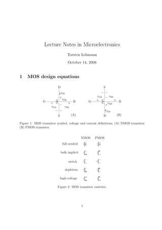
  • 1. Lecture Notes in Microelectronics Torsten Lehmann October 14, 2008 1 MOS design equations S B D G − + D B S G + vGS − + − vBS vDS + − + − vGS iDS vDS + iDS − vBS (B)(A) Figure 1: MOS transistor symbol, voltage and current definitions; (A) NMOS transistor (B) PMOS transistor. NMOS PMOS full symbol bulk implicit switch depletion high-voltage Figure 2: MOS transistor varieties. 1
  • 2. 1.1 Support equations threshold voltage Vth = Vth0 + γ |2φF − vBS| − |2φF| (1) n/p sign function |x|p ≡ x for n-channel −x for p-channel ; |x|p = γ |γ| x (2) sub-threshold slope n = γ 2 |2φF − vBS| + |1|p (3) gate-overdrive voltage vEff = vGS − Vth (4) velocity saturation µ = µ0 1 + vDS/(ECritL) (5) drain saturation voltage vDSsat = LECrit 1 + 2vEff/(LECrit) − 1 (6) ≃ vEff, |2vEff|p ≪ |LECrit|p (7) drain current factor β = W L K′ = W L µCox; K′ = µCox (8) channel-length modulation α = 1 + λvDS = 1 + kλvDS L ; λ = kλ L (9) thermal voltage VT = kT/q (10) sub-threshold scale current I0 = 1 2 µCox(2nVT )2 (11) weak-strong transition IWST = I0 ln2 (2) W L (12) 1.2 Current equations Strong inversion (|vEff|p >∼ |2nVT ln(10)|p, or |IDS,sat|p ≫ |IWST|p): iDS = µCox W L vEffvDS − 1 2 v2 DS α, |vDSsat|p > |vDS|p (triode) (13) iDS = IDS,sat = µCox W L vEffvDSsat − 1 2 v2 DSsat α, |vDSsat|p ≤ |vDS|p (saturation)(14) ≃ 1 2 µCox W L v2 Effα, |2vEff|p ≪ |LECrit|p (not velocity saturated) (15) ≃ µ0CoxECritW vEff − 1 2 vDSsat α, |2vEff|p ≫ |LECrit|p (deep velocity sat.) (16) Weak inversion (|vEff|p <∼ −|2nVT ln(10)|p, or |IDS,sat|p ≪ |IWST|p): iDS = I0 W L evEff /(nVT ) 1 − e−|vDS|p/VT α (17) iDS = IDS,sat = I0 W L evEff /(nVT ) α, |nVT |p ≪ |vDS|p (saturation) (18) Moderate inversion saturation (|vDS|p ≫ |nVT |p, and |vDS|p > |vEff|p): iDS = IDS,sat = 1 2 µCox W L (2nVT )2 ln2 1 + evEff /(2nVT ) α (19) 2
  • 3. 0.001 0.01 0.1 1 10 100 1000 -4 -2 0 2 4 iDS/Iwst veff/nVT current expression (log(1+exp(x/2))/log(2))**2 x**2/(log(2)*2)**2 exp(x)/log(2)**2 Figure 3: Normalised saturation current 1.3 Sample MOST parameters Typical parameters for some CMOS processes (preliminary): Process 0.35 µm 0.18 µm Parameter n-channel p-channel n-channel p-channel VDD,max 2.5 V 2.5 V 1.8 V 1.8 V Vth0 0.6 V −0.6 V 0.5 V −0.5 V γ 0.5 √ V −0.5 √ V 0.6 √ V −0.4 √ V 2φF 0.7 V −0.7 V 0.8 V −0.8 V n (zero bias) 1.3 −1.3 1.4 −1.3 Lmin 0.35 µm 0.35 µm 0.18 µm 0.18 µm kλ 0.1 µm/V −0.1 µm/V 0.12 µm/V −0.08 µm/V µ0Cox 120 µA/V2 −40 µA/V2 260 µA/V2 −65 µA/V2 Cox 4 fF/µm2 4 fF/µm2 8 fF/µm2 8 fF/µm2 Cj0 0.8 fF/µm2 1.2 fF/µm2 2 fF/µm2 2 fF/µm2 Cj0sw 0.3 fF/µm 0.4 fF/µm 0.6 fF/µm 0.6 fF/µm Cov 0.2 fF/µm 0.2 fF/µm 0.1 fF/µm 0.1 fF/µm xj 0.1 µm 0.1 µm 0.05 µm 0.05 µm ℓsd 1 µm 1 µm 0.5 µm 0.5 µm λ (DRC) 0.2 µm 0.2 µm 0.1 µm 0.1 µm ECrit ∞ −∞ 2.2 V/µm −5 V/µm 3
  • 4. 2 Noise Calculating total input referred noise is often impossible, as the integral typically diverges for both high frequencies (white noise) and low frequencies (1/f noise). The total output referred noise is easier, as any circuit has an upper band-width — typically, this doesn’t solve the 1/f divergence problem, however. My suggestion is to equate the lower frequency bound to 1/Tobs, where Tobs is the observation time of the system (e.g., the time it is turned on — say a day or so): V 2 no,tot = ∞ 1/Tobs i V 2 ni(f)|Hi(f)|2 df 3 Matching To a first order approximation, the relative variance of drain current in MOS transistor biased in strong inversion saturation can be expressed as: σ2 D I2 D = BW LW2 + BL WL2 + BK WL(µCox)2 + 4 BV WL(VGS − Vth)2 (20) where ID is the average (nominal) drain current, and the Bs are constants. For relatively large transistors and a given gate bias voltage, this simplifies to: σ2 D I2 D ≃ BI WL (21) 4
  • 5. 4 Problems 4.1 Problem 1 vOUT vIN IB VDD VSS Figure 4: Common source amplifier The common source amplifier in figure 4 is biased with a DC drain current of IB = 1 µA. It is to be implemented in the 0.35 µm process, where the smallest transistor dimensions allowed (for this amplifier) is 0.7 µm. • Find W and L such that the transistor is biased in weak inversion. Find for this transistor all the small-signal parameters (gm, rds, Cgs, Cgd, Csb, and Cdb) and the low-frequency voltage gain, Av. Find also fT for the transistor. • Now find W and L such that the transistor is biased in strong inversion, and again find gm, rds, Av and fT. For this amplifier, what must the DC bias value, VIN, of in the input voltage be? What must VIN be if the source voltage is 1 V rather than 0 V as on the figure? • Finally, find W and L such that the transistor is biased in strong inversion, but has the same gate area as the weak-inversion amplifier, and find gm, rds, Av and fT. 4.2 Problem 2 For the circuit in figure 5, prove that i1 − i2 = µCox W L v1v2 , when all transistors are identical and operate in the triode region (the bulk affect can be ignored). 4.3 Problem 3 For the CMOS nand-gate in figure 6, find all transistors widths, W and lengths, L such that the gate can drive a load capacitance of CL = 1 pF in less than 5 ns. 5
  • 6. 0V by feedbackv2 v1 i1 i2 Figure 5: Cross-coupled transistor pairs z a b CL N N PP DDV (a) param N P unit µCox 92 −30 µA/V2 Vth 0.8 −0.9 V Lmin 0.8 µm VDD 2 V (b) Figure 6: Static CMOS nand-gate (a) and circuit and transistor parameters (b) 4.4 Problem 4 a b z CL VB SN SN N P DDV Figure 7: CSL nand-gate For the Current Steering Logic (CSL) nand-gate in figure 7, find all transistors widths, W and lengths, L, and the bias voltage, VB such that the gate can drive a load capacitance of CL = 1 pF in less than 5 ns; use the same circuit and transistor parameters as in problem 3. 6
  • 7. 4.5 Problem 5 word line bit line MS MC VB (a) param val unit Cox 5 fF/µm2 Lmin 0.35 µm Cj(sb, sd) 1.5 fF · W VDD 3 V (b) Figure 8: DRAM cell (a) and transistor parameters The dynamic RAM cell in figure 8 is arranged in a square, 1 cm2 matrix. Estimate the largest number of bits in the matrix when the sense amplifier can detect a 50 mV voltage difference and relevant transistor parameters are given in the figure. Transistor ms is a switch transistor while transistor MC act as a storage capacitor. The bias voltage, VB is chosen > VDD + Vth, and the word-line is like-wise clock-boosted to a voltage > VDD + Vth when high. Find also the widths, W and lengths, L for the transistors. 4.6 Problem 6 iin iout Figure 9: Current mirror For a given vGS, the relative drain current variation (in saturation) is given by σ2 I2 D = BI WL , BI = 5 · 10−4 µm2 , where ID is the average drain current and σ2 is the variance of the drain current. The drain current is assumed to be normally distributed. For the current mirror in figure 9 with W/L = 5µm/2µm for both transistors, what is the probability that |iout − iin| < 1 %? 4.7 Problem 7 A wafer has a defect density of D = 0.01 cm−2 . Chips on the wafer are 2 cm2 in size, each having 1000 sub-components that perform outside specifications with a probability of 0.002 % each. Find the fraction of chips which function within specifications after manu- facturing. 7