SlideShare ist ein Scribd-Unternehmen logo
1 von 12
Explain the pin configuration of 8051 microcontroller. 5 marks
1. Pin diagram of 8051:
2. 8051 consists of 40 pins. There are four ports in 8051 microcontroller port0, port1, port2,
port3.
3. Total 32 pins are set aside for the four ports where each port takes 8 pins.
4. There are another pins like VCC, RST, XTAL2, XTAL1, GND, -EA/VPP, ALE/PROG and -
PSEN.
5. PORT 0:
ď‚· Port 0 is 8 bit bidirectional input output port.
ď‚· Port 0 pins can be used as high impedance pins.
ď‚· We are using pin numbers from 32 to 39.
ď‚· When used as an output the pin latches are programmed to 0.
ď‚· When used as an input the pin latches are programmed to 1.
6. PORT 1:
ď‚· Port 1 is 8 bit bidirectional input output port.
ď‚· Port 1 has no dual functions.
ď‚· We are using pin numbers from 1 to 9.
ď‚· When used as an output the pin latches are programmed to 0.
ď‚· When used as an input the pin latches are programmed to 1.
7. PORT 2:
ď‚· Port 2 is 8 bit bidirectional input output port.
ď‚· Port 2 emits the high address byte during fetches from external program memory and
during accesses to external data memory that use 16-bit addresses.
ď‚· We are using pin numbers from 21 to 29.
ď‚· When used as an output the pin latches are programmed to 0.
ď‚· When used as an input the pin latches are programmed to 1.
8. PORT 3:
ď‚· Port 3 is 8 bit bidirectional input output port.
ď‚· We are using pin numbers from 10 to 17.
ď‚· When used as an output the pin latches are programmed to 0.
ď‚· When used as an input the pin latches are programmed to 1.
9. VCC- VCC pin provides +5v supply to the 8051 microcontroller chip.
10. GND- this is ground pin.
11. RST- this is reset input pin.
12. XTAL 2- input to the inverting oscillator amplifier and internal clock circuit.
13. XTAL 1- output from the inverting oscillator amplifier.
14. Crystal may be connected between XTAL 2 and XTAL 1.
15. ALE/PROG- address latch enable pin.
16. PSEN- program store enable pin.
17. EA/VPP- external access enable pin.
18. 8051 consists of 4KB of on chip program memory and 128 bytes of on chip data memory.
19. 8051 has 64KB program external ROM and 64KB external RAM addressability.
20. The devices 8031, 8751 have the same pin-out, same timing and same electrical
characteristics as 8051.
Explain addressing modes of 8051 microcontroller. 10 marks
1. Addressing modes of 8051:
2. The ways by which address locations of data on which specific functions are performed while
microcontroller executes an instruction, are called as addressing modes.
3. Direct addressing mode:
i) In this mode the operand is specified by an 8 bit address field in the instruction.
ii) Example: MOV A,40H copy data from address 40H into A
MOV R0,14H copy data from address 14H into register R0
4. Indirect addressing mode:
i) In this addressing mode, the instruction specifies register which contains address of an
operand.
ii) Example: MOV A,@R1 copy the contents of memory location, whose address is specified in
R1 register to the accumulator
5. Register addressing mode:
i) Each register bank consists of registers R0 to R7. To access these registers there are special
instructions.
ii) Example: MOV A,R2 copy the data from register R2 to the selected register bank A
6. Register specific addressing:
i) In this addressing mode the instruction refers to a specific register such as accumulator or
data pointer DPTR.
ii) Example: DA A decimal adjust accumulator for addition
RR A rotate the contents of accumulator to right
7. Immediate addressing mode:
i) This method is the simplest method to get the data. In this addressing mode the source
operand is constant rather than a variable.
ii) Example: MOV A,#30H copy 30H immediately to accumulator
MOV P1,#0FFH copy FFH immediately to PORT1
MOV DPTR,#1234H copy 1234H immediately to DPTR
8. External addressing mode:
a) Code Access:
i) Using this instruction only external program memory can be accessed.
ii) Example: MOVC A,@A+DPTR this instruction will load the accumulator with the byte from
program memory
b) Data Access:
i) Using this instruction the programmer can access the external data memory.
ii) Example: MOVX @R0,A this instruction will copy the data from accumulator to external
memory location
Explain in detail ARM7 pipelining. 10M
1. The process of fetching the next instruction while the current instruction is being executed is
called as pipelining.
2. Pipelining is supported by the processor to increase speed of program execution.
3. Pipelining also increases throughput.
4. Many operations take place simultaneously in pipelining.
5. The pipelining has three stages FETCH, DECODE and EXECUTE.
6. Three stage pipeline:
7. FETCH: In this stage the ARM processor fetches the instruction from the memory.
8. DECODE: In this stage the ARM processor recognizes the instruction that is to be executed.
9. EXECUTE: In this stage the processor processes the instruction and writes the result back to
desired register.
10. These three stage of execution are overlapped, higher speed of execution will be achieved.
11. Once the pipeline is filled, each instruction requires one cycle to complete execution.
12. Single cycle instruction execution for a 3-stage pipeline in ARM7:
13. Multi cycle instruction execution for 3-stage pipeline in ARM7:
14. In case of single cycle instruction,
ď‚· In first cycle the processor fetches instruction 1 from the memory.
ď‚· In second cycle the processor fetches instruction 2 from the memory and decodes
instruction 1.
ď‚· In third cycle the processor fetches instruction 3 from the memory, decodes instruction 2
and executes instruction 1.
ď‚· In the fourth cycle the processor fetches instruction 4 from the memory, decodes
instruction 3 and executes instruction 2.
15. In single cycle execution the pipeline executes an instruction in three cycles i.e. it delivers a
throughput equal to one instruction per cycle.
16. In case of multi cycle instruction,
ď‚· Instruction 2 requires 4 clock cycles and hence the pipeline stalls for one clock pulse.
ď‚· The first instruction completes execution in the third clock pulse, while the second
instruction instead of completing execution in fourth clock pulse completes the same in
fifth clock pulse.
ď‚· Thereafter every instruction completes execution in one clock pulse.
17. The amount of work done at each stage can be reduced by increasing the number of stages
in the pipeline.
18. To improve the performance, the processor then can be operated at higher operating
frequency.
19. As ore number of cycles required filling the pipeline, the system latency also increases.
20. The data dependency between the stages can also be increased as the stages of pipeline
increase.
21. ARM7 processor consists of Register bank, Barrel shifter, ALU, Address register &
incrementer, Data register and Instruction decoder.
22. Register bank: This includes various registers.
23. Barrel shifter: Barrel shifter is used to do various operations.
24. The ALU: This is arithmetic logic unit. This unit performs various arithmetic and logical
operations.
25. Data registers: Data register is used as a buffer to store the data.
26. Instruction decoder: It decodes the instructions and it is associated with control logic.
Explain addressing modes of ARM7 processor. 10M
Answer:
Addressing modes of ARM7 processor:
Addressing modes for data processing operands:
1. Unmodified value:
i. In this addressing mode, the register or the value is given unmodified i.e. without any shift or
rotation.
ii. Example:
a. MOV R0,#1234H
This instruction will move the constant value (1234)10 into register R0.
b. MOV R0,R1
This instruction will move the value in register R1 to the register R0.
2. Modified value:
i. In this addressing mode the register or a value is shifted or rotated.
ii. Different shift and rotate operations:
a. Logical Shift Left (LSL):
MOV R0,R1,LSL#2
After the execution of this instruction R0 will become the value of R1shifted left by 2 bits.
b. Logical Shift Right (LSR):
MOV R0,R1,LSRR2
After the execution of this instructionR0 will have the value of R1 shifted right by R2 times.
c. Arithmetic Shift Right (ASR):
MOV R0,R1,ASR#2
After the execution of this instructionR0 will have the value of R1 arithmetic shifted right by 2
units.
d. Rotate Right (ROR):
This will take the value of register and rotate it right by n bits.
MOV R0,R1,RORR2
After the execution of this instructionR0 will have the value of R1 rotated right for R2 times.
e. Rotate Right Extended (RRX):
It is similar to rotate right through carry.
MOV R0,R1RRX
After the execution of this instructionR0 will have the value of R1 rotated right through carry by 1
bit.
Addressing modes for memory access operands:
1. Register indirect addressing mode:
i. In this addressing mode register is used to give the address of the memory location to be
accessed.
ii. LDR R0,[R1]
This instruction will load the register R0 with 32-bit word at the memory address held in the
register R1.
2. Relative register indirect addressing mode:
i. In this addressing mode the memory address is generated by an immediate value added to a
register. Pre index and post index are supported.
ii. LDR R0,[R1,#4]
This instruction will load the register R0 with the word at the memory address calculated by
adding by constant value 4 to the memory address contained in the R1 register.
3. Base indexed indirect addressing mode:
i. In this addressing mode the memory address is generated by adding the values of two
registers. Pre index and post index are supported.
ii. LDR R0,[R1,R2]
This instruction will load the register R0 with the word at the memory address calculated by
adding register R1 to register R2.
4. Base with scaled register addressing mode:
i. In this addressing mode the memory address is generated by a register value added to
another register shifted left. Pre index and post index are supported.
ii. LDR R0,[R1,R2,LSL#2]
This instruction will load the register R0 with the word at the memory address calculated by
adding register R1 with register R2 shifted left by 2 bits.
Difference between RISC and CISC 5/10M
No. RISC CISC
1 RISC stands for reduced instruction set
computing.
CISC stands for complex instruction set
computing.
2 In RISC number of instructions is less as
compare to CISC.
In CISC number of instructions is more as
compare to RISC.
3 Addressing modes are less in RISC. Addressing modes are more in CISC.
4 In RISC instruction formats are less
compare to CISC.
In CISC instruction formats are more
compare to RISC.
5 Control unit is hardwired in RISC. Control unit is micro-programmed in CISC.
6 Single CPU cycle requires executing an
instruction.
Multiple CPU cycle requires executing an
instruction.
7 Control unit and decoding subsystem is
simple in RISC.
Control unit and decoding subsystem is
complex.
8 RISC takes less time to design. CISC takes more time to design.
9 Complexity of compiler is simple in RISC. Complexity of compiler is complex in CISC.
10 HLL instructions are supported by RISC. HLL instructions are not supported by CISC.
11 The instruction size is small and it is fixed. The instruction size is big and it is variable.
12 The on chip CPU size is smaller, thus
there is space for cache.
There is no on chip space for cache.
13 The instruction set is compact, it can be
stored in on chip ROM.
External storage is needed for execution
instruction set.
14 The software and hardware manufacture
of RISC is simple.
The software and hardware manufacture of
CISC is complicated.
15 RISC’s are cheap as compare to CISC. CISC’s are expensive as compare to RISC.
Digital clock embedded system 5M/7M
1. LCD display, switches, micro-controller, power supply, clock circuit and reset pin are the
various components required for digital clock implementation.
2. Circuit diagram for digital clock implementation:
3. The above figure describes the standard circuit of digital clock for the 8051 microcontroller.
4. Circuit diagram for power supply of digital clock:
5. The power supply is implemented using transformer followed by regulator and rectifier.
6. The clock circuit of digital clock is implemented using standard circuit of 8051 which is
powered by INTEL.
7. The very important component of the digital clock is crystal.
8. The crystal of 12 MHz is used in between XTAL2 and XTAL1.
9. Circuit requires +5V power supply which is connected to VCC pin.
10. The various signals connected to the LCD display are power supply pins, VEE pin, data
pins, RS, RW and E pin.
11. RS pin is used to indicate a command to LCD.
12. RW pin is read or write operation to LCD.
13. E pin is called as enable pin. It is used to indicate the latching of data.
14. To do various operations on the timer such as, set the time and set the alarm the switch is
required.
Automated meter reading system 5M/10M
1. Block diagram of automated meter reading system:
2. The automated meter reading system is used to read power consumed and to generate the
power bill.
3. Power supply, clock or oscillator circuit, communication port (LCD display), current and
voltage sensors, ADC, modem, wireless AMR interface, program memory, data memory and
microcontroller are components used in automated meter reading system.
4. The power supply is implemented using transformer, rectifier and regulator.
5. Circuit diagram for power supply of AMR:
6. The clock circuit of digital clock is implemented using standard circuit of 8051 which is
powered by INTEL.
7. Power supply and crystal are very important components of the AMR system.
8. To implement serial communication easily 11.0592 MHz crystal is used.
9. Power supply, VEE pin, RS, RW, E pin and data pins are the various signals connected to the
LCD.
10. To measure the current, current sensor is used.
11. To measure the voltage, voltage sensor is used.
12. The arrangement of all these components will give result of the power consumed.
13. Wireless AMR interface is used for communication purpose.
14. To get the information from the system about the power consumption RE reader and
receiver is used.
15. The mechanism of the Automated Meter Reading System is implemented to transfer the
data over the power line and receiving in the office of the power provider.

Weitere ähnliche Inhalte

Was ist angesagt?

Assemblers: Ch03
Assemblers: Ch03Assemblers: Ch03
Assemblers: Ch03desta_gebre
 
Timing Diagram.pptx
Timing Diagram.pptxTiming Diagram.pptx
Timing Diagram.pptxISMT College
 
Addressing modes of 8051
Addressing modes of 8051Addressing modes of 8051
Addressing modes of 8051SARITHA REDDY
 
FSM and ASM
FSM and ASMFSM and ASM
FSM and ASMUnsa Shakir
 
Assembly Language Programming Of 8085
Assembly Language Programming Of 8085Assembly Language Programming Of 8085
Assembly Language Programming Of 8085techbed
 
Addressing modes of 8086
Addressing modes of 8086Addressing modes of 8086
Addressing modes of 8086Dr. AISHWARYA N
 
Assembler directives and basic steps ALP of 8086
Assembler directives and basic steps ALP of 8086Assembler directives and basic steps ALP of 8086
Assembler directives and basic steps ALP of 8086Urvashi Singh
 
Cache performance considerations
Cache performance considerationsCache performance considerations
Cache performance considerationsSlideshare
 
30. 8086 microprocessor pipelined architecture
30. 8086 microprocessor pipelined architecture30. 8086 microprocessor pipelined architecture
30. 8086 microprocessor pipelined architecturesandip das
 
Ch 1 introduction to Embedded Systems (AY:2018-2019--> First Semester)
Ch 1 introduction to Embedded Systems (AY:2018-2019--> First Semester)Ch 1 introduction to Embedded Systems (AY:2018-2019--> First Semester)
Ch 1 introduction to Embedded Systems (AY:2018-2019--> First Semester)Moe Moe Myint
 
Stacks & subroutines 1
Stacks & subroutines 1Stacks & subroutines 1
Stacks & subroutines 1deval patel
 
Instruction set of 8086
Instruction set of 8086Instruction set of 8086
Instruction set of 80869840596838
 
I/O port programming in 8051
I/O port programming in 8051I/O port programming in 8051
I/O port programming in 8051ssuser3a47cb
 
instruction cycle ppt
instruction cycle pptinstruction cycle ppt
instruction cycle pptsheetal singh
 
Programmableperipheralinterface 8255 ppt
Programmableperipheralinterface 8255 pptProgrammableperipheralinterface 8255 ppt
Programmableperipheralinterface 8255 pptsharan Kumar
 

Was ist angesagt? (20)

Assemblers: Ch03
Assemblers: Ch03Assemblers: Ch03
Assemblers: Ch03
 
Modes of transfer
Modes of transferModes of transfer
Modes of transfer
 
Timing Diagram.pptx
Timing Diagram.pptxTiming Diagram.pptx
Timing Diagram.pptx
 
Addressing modes of 8051
Addressing modes of 8051Addressing modes of 8051
Addressing modes of 8051
 
FSM and ASM
FSM and ASMFSM and ASM
FSM and ASM
 
Assembly Language Programming Of 8085
Assembly Language Programming Of 8085Assembly Language Programming Of 8085
Assembly Language Programming Of 8085
 
Addressing modes of 8086
Addressing modes of 8086Addressing modes of 8086
Addressing modes of 8086
 
Assembler directives and basic steps ALP of 8086
Assembler directives and basic steps ALP of 8086Assembler directives and basic steps ALP of 8086
Assembler directives and basic steps ALP of 8086
 
Cache performance considerations
Cache performance considerationsCache performance considerations
Cache performance considerations
 
Register Organization of 80386
Register Organization of 80386Register Organization of 80386
Register Organization of 80386
 
30. 8086 microprocessor pipelined architecture
30. 8086 microprocessor pipelined architecture30. 8086 microprocessor pipelined architecture
30. 8086 microprocessor pipelined architecture
 
Ch 1 introduction to Embedded Systems (AY:2018-2019--> First Semester)
Ch 1 introduction to Embedded Systems (AY:2018-2019--> First Semester)Ch 1 introduction to Embedded Systems (AY:2018-2019--> First Semester)
Ch 1 introduction to Embedded Systems (AY:2018-2019--> First Semester)
 
8253
82538253
8253
 
Stacks & subroutines 1
Stacks & subroutines 1Stacks & subroutines 1
Stacks & subroutines 1
 
Instruction set of 8086
Instruction set of 8086Instruction set of 8086
Instruction set of 8086
 
Shift Register
Shift RegisterShift Register
Shift Register
 
I/O port programming in 8051
I/O port programming in 8051I/O port programming in 8051
I/O port programming in 8051
 
instruction cycle ppt
instruction cycle pptinstruction cycle ppt
instruction cycle ppt
 
IO buffering
IO bufferingIO buffering
IO buffering
 
Programmableperipheralinterface 8255 ppt
Programmableperipheralinterface 8255 pptProgrammableperipheralinterface 8255 ppt
Programmableperipheralinterface 8255 ppt
 

Ă„hnlich wie 8051 microcontroller

Micro controller(pratheesh)
Micro controller(pratheesh)Micro controller(pratheesh)
Micro controller(pratheesh)Pratheesh Pala
 
Unit II arm 7 Instruction Set
Unit II arm 7 Instruction SetUnit II arm 7 Instruction Set
Unit II arm 7 Instruction SetDr. Pankaj Zope
 
Lecture 4 (8051 instruction set) rv01
Lecture 4 (8051 instruction set) rv01Lecture 4 (8051 instruction set) rv01
Lecture 4 (8051 instruction set) rv01cairo university
 
Xcs 234 microprocessors
Xcs 234 microprocessorsXcs 234 microprocessors
Xcs 234 microprocessorssweta suman
 
Https _doc-0o-c4-apps-viewer.googleusercontent
Https  _doc-0o-c4-apps-viewer.googleusercontent Https  _doc-0o-c4-apps-viewer.googleusercontent
Https _doc-0o-c4-apps-viewer.googleusercontent vijaydeepakg
 
Unit iv introduction to 8051 microcontroller ppts
Unit iv introduction to 8051 microcontroller pptsUnit iv introduction to 8051 microcontroller ppts
Unit iv introduction to 8051 microcontroller pptsSreenivas Hanumandla
 
assignment 1-MC.pdf
assignment 1-MC.pdfassignment 1-MC.pdf
assignment 1-MC.pdfSANTHAKUMARP5
 
microcontroller_instruction_set for ENGINEERING STUDENTS
microcontroller_instruction_set for  ENGINEERING STUDENTSmicrocontroller_instruction_set for  ENGINEERING STUDENTS
microcontroller_instruction_set for ENGINEERING STUDENTSssuser2b759d
 
Qb microprocessors
Qb microprocessorsQb microprocessors
Qb microprocessorsNeelam Kapoor
 
module-3.pptx
module-3.pptxmodule-3.pptx
module-3.pptxAmbika Naik
 
timing_diagram_of_8085.pptx
timing_diagram_of_8085.pptxtiming_diagram_of_8085.pptx
timing_diagram_of_8085.pptxBhagyarajKosamia
 
Memory intrface and addrs modes
Memory intrface and addrs modesMemory intrface and addrs modes
Memory intrface and addrs modesbalbirvirdi
 
Design and Fabrication of 4-bit processor
Design and Fabrication of  4-bit processorDesign and Fabrication of  4-bit processor
Design and Fabrication of 4-bit processorPriyatham Bollimpalli
 
Module 2 instruction set
Module 2 instruction set Module 2 instruction set
Module 2 instruction set Deepak John
 

Ă„hnlich wie 8051 microcontroller (20)

Micro controller(pratheesh)
Micro controller(pratheesh)Micro controller(pratheesh)
Micro controller(pratheesh)
 
Addressing modes
Addressing modesAddressing modes
Addressing modes
 
Unit II arm 7 Instruction Set
Unit II arm 7 Instruction SetUnit II arm 7 Instruction Set
Unit II arm 7 Instruction Set
 
8051 microcontroller
8051 microcontroller8051 microcontroller
8051 microcontroller
 
Lecture 4 (8051 instruction set) rv01
Lecture 4 (8051 instruction set) rv01Lecture 4 (8051 instruction set) rv01
Lecture 4 (8051 instruction set) rv01
 
Xcs 234 microprocessors
Xcs 234 microprocessorsXcs 234 microprocessors
Xcs 234 microprocessors
 
Https _doc-0o-c4-apps-viewer.googleusercontent
Https  _doc-0o-c4-apps-viewer.googleusercontent Https  _doc-0o-c4-apps-viewer.googleusercontent
Https _doc-0o-c4-apps-viewer.googleusercontent
 
Unit iv introduction to 8051 microcontroller ppts
Unit iv introduction to 8051 microcontroller pptsUnit iv introduction to 8051 microcontroller ppts
Unit iv introduction to 8051 microcontroller ppts
 
Mpi lab manual eee
Mpi lab manual eeeMpi lab manual eee
Mpi lab manual eee
 
assignment 1-MC.pdf
assignment 1-MC.pdfassignment 1-MC.pdf
assignment 1-MC.pdf
 
microcontroller_instruction_set for ENGINEERING STUDENTS
microcontroller_instruction_set for  ENGINEERING STUDENTSmicrocontroller_instruction_set for  ENGINEERING STUDENTS
microcontroller_instruction_set for ENGINEERING STUDENTS
 
Qb microprocessors
Qb microprocessorsQb microprocessors
Qb microprocessors
 
module-3.pptx
module-3.pptxmodule-3.pptx
module-3.pptx
 
addressingmodes8051.ppt
addressingmodes8051.pptaddressingmodes8051.ppt
addressingmodes8051.ppt
 
8051d
8051d8051d
8051d
 
Pdemodule 4
Pdemodule 4Pdemodule 4
Pdemodule 4
 
timing_diagram_of_8085.pptx
timing_diagram_of_8085.pptxtiming_diagram_of_8085.pptx
timing_diagram_of_8085.pptx
 
Memory intrface and addrs modes
Memory intrface and addrs modesMemory intrface and addrs modes
Memory intrface and addrs modes
 
Design and Fabrication of 4-bit processor
Design and Fabrication of  4-bit processorDesign and Fabrication of  4-bit processor
Design and Fabrication of 4-bit processor
 
Module 2 instruction set
Module 2 instruction set Module 2 instruction set
Module 2 instruction set
 

Mehr von chirag patil

Wh Yes-No questions.pptx
Wh Yes-No questions.pptxWh Yes-No questions.pptx
Wh Yes-No questions.pptxchirag patil
 
joining words not only but also.pptx
joining words not only but also.pptxjoining words not only but also.pptx
joining words not only but also.pptxchirag patil
 
Basic English Grammar 2.pptx
Basic English Grammar 2.pptxBasic English Grammar 2.pptx
Basic English Grammar 2.pptxchirag patil
 
Basic English Grammar.pptx
Basic English Grammar.pptxBasic English Grammar.pptx
Basic English Grammar.pptxchirag patil
 
Maths formulae
Maths formulaeMaths formulae
Maths formulaechirag patil
 
Input output devices
Input output devicesInput output devices
Input output deviceschirag patil
 
Shortcut keys
Shortcut keysShortcut keys
Shortcut keyschirag patil
 
Operating system
Operating systemOperating system
Operating systemchirag patil
 
Network topology
Network topologyNetwork topology
Network topologychirag patil
 
Decimal and binary conversion
Decimal and binary conversionDecimal and binary conversion
Decimal and binary conversionchirag patil
 
Abbreviations and full forms
Abbreviations and full formsAbbreviations and full forms
Abbreviations and full formschirag patil
 
Web engineering and Technology
Web engineering and TechnologyWeb engineering and Technology
Web engineering and Technologychirag patil
 
Web data management
Web data managementWeb data management
Web data managementchirag patil
 
Web application development
Web application developmentWeb application development
Web application developmentchirag patil
 
Programming the web
Programming the webProgramming the web
Programming the webchirag patil
 
Operating System
Operating SystemOperating System
Operating Systemchirag patil
 
Computer Graphics and Virtual Reality
Computer Graphics and Virtual RealityComputer Graphics and Virtual Reality
Computer Graphics and Virtual Realitychirag patil
 
Advanced Database Management Syatem
Advanced Database Management SyatemAdvanced Database Management Syatem
Advanced Database Management Syatemchirag patil
 
The law of attraction for positive things
The law of attraction for positive thingsThe law of attraction for positive things
The law of attraction for positive thingschirag patil
 

Mehr von chirag patil (20)

Wh Yes-No questions.pptx
Wh Yes-No questions.pptxWh Yes-No questions.pptx
Wh Yes-No questions.pptx
 
joining words not only but also.pptx
joining words not only but also.pptxjoining words not only but also.pptx
joining words not only but also.pptx
 
Basic English Grammar 2.pptx
Basic English Grammar 2.pptxBasic English Grammar 2.pptx
Basic English Grammar 2.pptx
 
Basic English Grammar.pptx
Basic English Grammar.pptxBasic English Grammar.pptx
Basic English Grammar.pptx
 
Maths formulae
Maths formulaeMaths formulae
Maths formulae
 
Input output devices
Input output devicesInput output devices
Input output devices
 
Shortcut keys
Shortcut keysShortcut keys
Shortcut keys
 
Operating system
Operating systemOperating system
Operating system
 
Network topology
Network topologyNetwork topology
Network topology
 
Decimal and binary conversion
Decimal and binary conversionDecimal and binary conversion
Decimal and binary conversion
 
Abbreviations and full forms
Abbreviations and full formsAbbreviations and full forms
Abbreviations and full forms
 
ASCII Code
ASCII CodeASCII Code
ASCII Code
 
Web engineering and Technology
Web engineering and TechnologyWeb engineering and Technology
Web engineering and Technology
 
Web data management
Web data managementWeb data management
Web data management
 
Web application development
Web application developmentWeb application development
Web application development
 
Programming the web
Programming the webProgramming the web
Programming the web
 
Operating System
Operating SystemOperating System
Operating System
 
Computer Graphics and Virtual Reality
Computer Graphics and Virtual RealityComputer Graphics and Virtual Reality
Computer Graphics and Virtual Reality
 
Advanced Database Management Syatem
Advanced Database Management SyatemAdvanced Database Management Syatem
Advanced Database Management Syatem
 
The law of attraction for positive things
The law of attraction for positive thingsThe law of attraction for positive things
The law of attraction for positive things
 

KĂĽrzlich hochgeladen

CCS355 Neural Networks & Deep Learning Unit 1 PDF notes with Question bank .pdf
CCS355 Neural Networks & Deep Learning Unit 1 PDF notes with Question bank .pdfCCS355 Neural Networks & Deep Learning Unit 1 PDF notes with Question bank .pdf
CCS355 Neural Networks & Deep Learning Unit 1 PDF notes with Question bank .pdfAsst.prof M.Gokilavani
 
An experimental study in using natural admixture as an alternative for chemic...
An experimental study in using natural admixture as an alternative for chemic...An experimental study in using natural admixture as an alternative for chemic...
An experimental study in using natural admixture as an alternative for chemic...Chandu841456
 
Decoding Kotlin - Your guide to solving the mysterious in Kotlin.pptx
Decoding Kotlin - Your guide to solving the mysterious in Kotlin.pptxDecoding Kotlin - Your guide to solving the mysterious in Kotlin.pptx
Decoding Kotlin - Your guide to solving the mysterious in Kotlin.pptxJoĂŁo Esperancinha
 
Architect Hassan Khalil Portfolio for 2024
Architect Hassan Khalil Portfolio for 2024Architect Hassan Khalil Portfolio for 2024
Architect Hassan Khalil Portfolio for 2024hassan khalil
 
computer application and construction management
computer application and construction managementcomputer application and construction management
computer application and construction managementMariconPadriquez1
 
What are the advantages and disadvantages of membrane structures.pptx
What are the advantages and disadvantages of membrane structures.pptxWhat are the advantages and disadvantages of membrane structures.pptx
What are the advantages and disadvantages of membrane structures.pptxwendy cai
 
Introduction to Machine Learning Unit-3 for II MECH
Introduction to Machine Learning Unit-3 for II MECHIntroduction to Machine Learning Unit-3 for II MECH
Introduction to Machine Learning Unit-3 for II MECHC Sai Kiran
 
Risk Assessment For Installation of Drainage Pipes.pdf
Risk Assessment For Installation of Drainage Pipes.pdfRisk Assessment For Installation of Drainage Pipes.pdf
Risk Assessment For Installation of Drainage Pipes.pdfROCENODodongVILLACER
 
Gfe Mayur Vihar Call Girls Service WhatsApp -> 9999965857 Available 24x7 ^ De...
Gfe Mayur Vihar Call Girls Service WhatsApp -> 9999965857 Available 24x7 ^ De...Gfe Mayur Vihar Call Girls Service WhatsApp -> 9999965857 Available 24x7 ^ De...
Gfe Mayur Vihar Call Girls Service WhatsApp -> 9999965857 Available 24x7 ^ De...srsj9000
 
UNIT III ANALOG ELECTRONICS (BASIC ELECTRONICS)
UNIT III ANALOG ELECTRONICS (BASIC ELECTRONICS)UNIT III ANALOG ELECTRONICS (BASIC ELECTRONICS)
UNIT III ANALOG ELECTRONICS (BASIC ELECTRONICS)Dr SOUNDIRARAJ N
 
Call Girls Narol 7397865700 Independent Call Girls
Call Girls Narol 7397865700 Independent Call GirlsCall Girls Narol 7397865700 Independent Call Girls
Call Girls Narol 7397865700 Independent Call Girlsssuser7cb4ff
 
Why does (not) Kafka need fsync: Eliminating tail latency spikes caused by fsync
Why does (not) Kafka need fsync: Eliminating tail latency spikes caused by fsyncWhy does (not) Kafka need fsync: Eliminating tail latency spikes caused by fsync
Why does (not) Kafka need fsync: Eliminating tail latency spikes caused by fsyncssuser2ae721
 
Call Us ≽ 8377877756 ≼ Call Girls In Shastri Nagar (Delhi)
Call Us ≽ 8377877756 ≼ Call Girls In Shastri Nagar (Delhi)Call Us ≽ 8377877756 ≼ Call Girls In Shastri Nagar (Delhi)
Call Us ≽ 8377877756 ≼ Call Girls In Shastri Nagar (Delhi)dollysharma2066
 
Work Experience-Dalton Park.pptxfvvvvvvv
Work Experience-Dalton Park.pptxfvvvvvvvWork Experience-Dalton Park.pptxfvvvvvvv
Work Experience-Dalton Park.pptxfvvvvvvvLewisJB
 
Study on Air-Water & Water-Water Heat Exchange in a Finned Tube Exchanger
Study on Air-Water & Water-Water Heat Exchange in a Finned Tube ExchangerStudy on Air-Water & Water-Water Heat Exchange in a Finned Tube Exchanger
Study on Air-Water & Water-Water Heat Exchange in a Finned Tube ExchangerAnamika Sarkar
 
main PPT.pptx of girls hostel security using rfid
main PPT.pptx of girls hostel security using rfidmain PPT.pptx of girls hostel security using rfid
main PPT.pptx of girls hostel security using rfidNikhilNagaraju
 

KĂĽrzlich hochgeladen (20)

CCS355 Neural Networks & Deep Learning Unit 1 PDF notes with Question bank .pdf
CCS355 Neural Networks & Deep Learning Unit 1 PDF notes with Question bank .pdfCCS355 Neural Networks & Deep Learning Unit 1 PDF notes with Question bank .pdf
CCS355 Neural Networks & Deep Learning Unit 1 PDF notes with Question bank .pdf
 
An experimental study in using natural admixture as an alternative for chemic...
An experimental study in using natural admixture as an alternative for chemic...An experimental study in using natural admixture as an alternative for chemic...
An experimental study in using natural admixture as an alternative for chemic...
 
Decoding Kotlin - Your guide to solving the mysterious in Kotlin.pptx
Decoding Kotlin - Your guide to solving the mysterious in Kotlin.pptxDecoding Kotlin - Your guide to solving the mysterious in Kotlin.pptx
Decoding Kotlin - Your guide to solving the mysterious in Kotlin.pptx
 
Architect Hassan Khalil Portfolio for 2024
Architect Hassan Khalil Portfolio for 2024Architect Hassan Khalil Portfolio for 2024
Architect Hassan Khalil Portfolio for 2024
 
computer application and construction management
computer application and construction managementcomputer application and construction management
computer application and construction management
 
What are the advantages and disadvantages of membrane structures.pptx
What are the advantages and disadvantages of membrane structures.pptxWhat are the advantages and disadvantages of membrane structures.pptx
What are the advantages and disadvantages of membrane structures.pptx
 
Introduction to Machine Learning Unit-3 for II MECH
Introduction to Machine Learning Unit-3 for II MECHIntroduction to Machine Learning Unit-3 for II MECH
Introduction to Machine Learning Unit-3 for II MECH
 
Risk Assessment For Installation of Drainage Pipes.pdf
Risk Assessment For Installation of Drainage Pipes.pdfRisk Assessment For Installation of Drainage Pipes.pdf
Risk Assessment For Installation of Drainage Pipes.pdf
 
Gfe Mayur Vihar Call Girls Service WhatsApp -> 9999965857 Available 24x7 ^ De...
Gfe Mayur Vihar Call Girls Service WhatsApp -> 9999965857 Available 24x7 ^ De...Gfe Mayur Vihar Call Girls Service WhatsApp -> 9999965857 Available 24x7 ^ De...
Gfe Mayur Vihar Call Girls Service WhatsApp -> 9999965857 Available 24x7 ^ De...
 
young call girls in Green Park🔝 9953056974 🔝 escort Service
young call girls in Green Park🔝 9953056974 🔝 escort Serviceyoung call girls in Green Park🔝 9953056974 🔝 escort Service
young call girls in Green Park🔝 9953056974 🔝 escort Service
 
UNIT III ANALOG ELECTRONICS (BASIC ELECTRONICS)
UNIT III ANALOG ELECTRONICS (BASIC ELECTRONICS)UNIT III ANALOG ELECTRONICS (BASIC ELECTRONICS)
UNIT III ANALOG ELECTRONICS (BASIC ELECTRONICS)
 
POWER SYSTEMS-1 Complete notes examples
POWER SYSTEMS-1 Complete notes  examplesPOWER SYSTEMS-1 Complete notes  examples
POWER SYSTEMS-1 Complete notes examples
 
Call Girls Narol 7397865700 Independent Call Girls
Call Girls Narol 7397865700 Independent Call GirlsCall Girls Narol 7397865700 Independent Call Girls
Call Girls Narol 7397865700 Independent Call Girls
 
Why does (not) Kafka need fsync: Eliminating tail latency spikes caused by fsync
Why does (not) Kafka need fsync: Eliminating tail latency spikes caused by fsyncWhy does (not) Kafka need fsync: Eliminating tail latency spikes caused by fsync
Why does (not) Kafka need fsync: Eliminating tail latency spikes caused by fsync
 
Design and analysis of solar grass cutter.pdf
Design and analysis of solar grass cutter.pdfDesign and analysis of solar grass cutter.pdf
Design and analysis of solar grass cutter.pdf
 
Call Us ≽ 8377877756 ≼ Call Girls In Shastri Nagar (Delhi)
Call Us ≽ 8377877756 ≼ Call Girls In Shastri Nagar (Delhi)Call Us ≽ 8377877756 ≼ Call Girls In Shastri Nagar (Delhi)
Call Us ≽ 8377877756 ≼ Call Girls In Shastri Nagar (Delhi)
 
Work Experience-Dalton Park.pptxfvvvvvvv
Work Experience-Dalton Park.pptxfvvvvvvvWork Experience-Dalton Park.pptxfvvvvvvv
Work Experience-Dalton Park.pptxfvvvvvvv
 
young call girls in Rajiv Chowk🔝 9953056974 🔝 Delhi escort Service
young call girls in Rajiv Chowk🔝 9953056974 🔝 Delhi escort Serviceyoung call girls in Rajiv Chowk🔝 9953056974 🔝 Delhi escort Service
young call girls in Rajiv Chowk🔝 9953056974 🔝 Delhi escort Service
 
Study on Air-Water & Water-Water Heat Exchange in a Finned Tube Exchanger
Study on Air-Water & Water-Water Heat Exchange in a Finned Tube ExchangerStudy on Air-Water & Water-Water Heat Exchange in a Finned Tube Exchanger
Study on Air-Water & Water-Water Heat Exchange in a Finned Tube Exchanger
 
main PPT.pptx of girls hostel security using rfid
main PPT.pptx of girls hostel security using rfidmain PPT.pptx of girls hostel security using rfid
main PPT.pptx of girls hostel security using rfid
 

8051 microcontroller

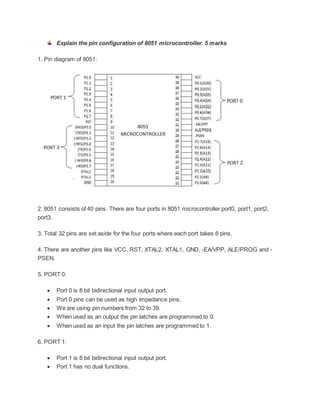
  • 1. Explain the pin configuration of 8051 microcontroller. 5 marks 1. Pin diagram of 8051: 2. 8051 consists of 40 pins. There are four ports in 8051 microcontroller port0, port1, port2, port3. 3. Total 32 pins are set aside for the four ports where each port takes 8 pins. 4. There are another pins like VCC, RST, XTAL2, XTAL1, GND, -EA/VPP, ALE/PROG and - PSEN. 5. PORT 0: ď‚· Port 0 is 8 bit bidirectional input output port. ď‚· Port 0 pins can be used as high impedance pins. ď‚· We are using pin numbers from 32 to 39. ď‚· When used as an output the pin latches are programmed to 0. ď‚· When used as an input the pin latches are programmed to 1. 6. PORT 1: ď‚· Port 1 is 8 bit bidirectional input output port. ď‚· Port 1 has no dual functions.
  • 2. ď‚· We are using pin numbers from 1 to 9. ď‚· When used as an output the pin latches are programmed to 0. ď‚· When used as an input the pin latches are programmed to 1. 7. PORT 2: ď‚· Port 2 is 8 bit bidirectional input output port. ď‚· Port 2 emits the high address byte during fetches from external program memory and during accesses to external data memory that use 16-bit addresses. ď‚· We are using pin numbers from 21 to 29. ď‚· When used as an output the pin latches are programmed to 0. ď‚· When used as an input the pin latches are programmed to 1. 8. PORT 3: ď‚· Port 3 is 8 bit bidirectional input output port. ď‚· We are using pin numbers from 10 to 17. ď‚· When used as an output the pin latches are programmed to 0. ď‚· When used as an input the pin latches are programmed to 1. 9. VCC- VCC pin provides +5v supply to the 8051 microcontroller chip. 10. GND- this is ground pin. 11. RST- this is reset input pin. 12. XTAL 2- input to the inverting oscillator amplifier and internal clock circuit. 13. XTAL 1- output from the inverting oscillator amplifier. 14. Crystal may be connected between XTAL 2 and XTAL 1. 15. ALE/PROG- address latch enable pin. 16. PSEN- program store enable pin. 17. EA/VPP- external access enable pin. 18. 8051 consists of 4KB of on chip program memory and 128 bytes of on chip data memory. 19. 8051 has 64KB program external ROM and 64KB external RAM addressability.
  • 3. 20. The devices 8031, 8751 have the same pin-out, same timing and same electrical characteristics as 8051. Explain addressing modes of 8051 microcontroller. 10 marks 1. Addressing modes of 8051: 2. The ways by which address locations of data on which specific functions are performed while microcontroller executes an instruction, are called as addressing modes. 3. Direct addressing mode: i) In this mode the operand is specified by an 8 bit address field in the instruction. ii) Example: MOV A,40H copy data from address 40H into A MOV R0,14H copy data from address 14H into register R0 4. Indirect addressing mode: i) In this addressing mode, the instruction specifies register which contains address of an operand. ii) Example: MOV A,@R1 copy the contents of memory location, whose address is specified in R1 register to the accumulator 5. Register addressing mode: i) Each register bank consists of registers R0 to R7. To access these registers there are special instructions. ii) Example: MOV A,R2 copy the data from register R2 to the selected register bank A
  • 4. 6. Register specific addressing: i) In this addressing mode the instruction refers to a specific register such as accumulator or data pointer DPTR. ii) Example: DA A decimal adjust accumulator for addition RR A rotate the contents of accumulator to right 7. Immediate addressing mode: i) This method is the simplest method to get the data. In this addressing mode the source operand is constant rather than a variable. ii) Example: MOV A,#30H copy 30H immediately to accumulator MOV P1,#0FFH copy FFH immediately to PORT1 MOV DPTR,#1234H copy 1234H immediately to DPTR 8. External addressing mode: a) Code Access: i) Using this instruction only external program memory can be accessed. ii) Example: MOVC A,@A+DPTR this instruction will load the accumulator with the byte from program memory b) Data Access: i) Using this instruction the programmer can access the external data memory. ii) Example: MOVX @R0,A this instruction will copy the data from accumulator to external memory location Explain in detail ARM7 pipelining. 10M 1. The process of fetching the next instruction while the current instruction is being executed is called as pipelining. 2. Pipelining is supported by the processor to increase speed of program execution. 3. Pipelining also increases throughput. 4. Many operations take place simultaneously in pipelining. 5. The pipelining has three stages FETCH, DECODE and EXECUTE.
  • 5. 6. Three stage pipeline: 7. FETCH: In this stage the ARM processor fetches the instruction from the memory. 8. DECODE: In this stage the ARM processor recognizes the instruction that is to be executed. 9. EXECUTE: In this stage the processor processes the instruction and writes the result back to desired register. 10. These three stage of execution are overlapped, higher speed of execution will be achieved. 11. Once the pipeline is filled, each instruction requires one cycle to complete execution. 12. Single cycle instruction execution for a 3-stage pipeline in ARM7: 13. Multi cycle instruction execution for 3-stage pipeline in ARM7:
  • 6. 14. In case of single cycle instruction, ď‚· In first cycle the processor fetches instruction 1 from the memory. ď‚· In second cycle the processor fetches instruction 2 from the memory and decodes instruction 1. ď‚· In third cycle the processor fetches instruction 3 from the memory, decodes instruction 2 and executes instruction 1. ď‚· In the fourth cycle the processor fetches instruction 4 from the memory, decodes instruction 3 and executes instruction 2. 15. In single cycle execution the pipeline executes an instruction in three cycles i.e. it delivers a throughput equal to one instruction per cycle. 16. In case of multi cycle instruction, ď‚· Instruction 2 requires 4 clock cycles and hence the pipeline stalls for one clock pulse. ď‚· The first instruction completes execution in the third clock pulse, while the second instruction instead of completing execution in fourth clock pulse completes the same in fifth clock pulse. ď‚· Thereafter every instruction completes execution in one clock pulse. 17. The amount of work done at each stage can be reduced by increasing the number of stages in the pipeline. 18. To improve the performance, the processor then can be operated at higher operating frequency. 19. As ore number of cycles required filling the pipeline, the system latency also increases. 20. The data dependency between the stages can also be increased as the stages of pipeline increase. 21. ARM7 processor consists of Register bank, Barrel shifter, ALU, Address register & incrementer, Data register and Instruction decoder. 22. Register bank: This includes various registers. 23. Barrel shifter: Barrel shifter is used to do various operations. 24. The ALU: This is arithmetic logic unit. This unit performs various arithmetic and logical operations. 25. Data registers: Data register is used as a buffer to store the data. 26. Instruction decoder: It decodes the instructions and it is associated with control logic. Explain addressing modes of ARM7 processor. 10M Answer:
  • 7. Addressing modes of ARM7 processor: Addressing modes for data processing operands: 1. Unmodified value: i. In this addressing mode, the register or the value is given unmodified i.e. without any shift or rotation. ii. Example: a. MOV R0,#1234H This instruction will move the constant value (1234)10 into register R0. b. MOV R0,R1 This instruction will move the value in register R1 to the register R0. 2. Modified value: i. In this addressing mode the register or a value is shifted or rotated. ii. Different shift and rotate operations: a. Logical Shift Left (LSL): MOV R0,R1,LSL#2 After the execution of this instruction R0 will become the value of R1shifted left by 2 bits. b. Logical Shift Right (LSR): MOV R0,R1,LSRR2 After the execution of this instructionR0 will have the value of R1 shifted right by R2 times.
  • 8. c. Arithmetic Shift Right (ASR): MOV R0,R1,ASR#2 After the execution of this instructionR0 will have the value of R1 arithmetic shifted right by 2 units. d. Rotate Right (ROR): This will take the value of register and rotate it right by n bits. MOV R0,R1,RORR2 After the execution of this instructionR0 will have the value of R1 rotated right for R2 times. e. Rotate Right Extended (RRX): It is similar to rotate right through carry. MOV R0,R1RRX After the execution of this instructionR0 will have the value of R1 rotated right through carry by 1 bit. Addressing modes for memory access operands: 1. Register indirect addressing mode: i. In this addressing mode register is used to give the address of the memory location to be accessed. ii. LDR R0,[R1] This instruction will load the register R0 with 32-bit word at the memory address held in the register R1. 2. Relative register indirect addressing mode: i. In this addressing mode the memory address is generated by an immediate value added to a register. Pre index and post index are supported. ii. LDR R0,[R1,#4] This instruction will load the register R0 with the word at the memory address calculated by adding by constant value 4 to the memory address contained in the R1 register. 3. Base indexed indirect addressing mode: i. In this addressing mode the memory address is generated by adding the values of two registers. Pre index and post index are supported.
  • 9. ii. LDR R0,[R1,R2] This instruction will load the register R0 with the word at the memory address calculated by adding register R1 to register R2. 4. Base with scaled register addressing mode: i. In this addressing mode the memory address is generated by a register value added to another register shifted left. Pre index and post index are supported. ii. LDR R0,[R1,R2,LSL#2] This instruction will load the register R0 with the word at the memory address calculated by adding register R1 with register R2 shifted left by 2 bits. Difference between RISC and CISC 5/10M No. RISC CISC 1 RISC stands for reduced instruction set computing. CISC stands for complex instruction set computing. 2 In RISC number of instructions is less as compare to CISC. In CISC number of instructions is more as compare to RISC. 3 Addressing modes are less in RISC. Addressing modes are more in CISC. 4 In RISC instruction formats are less compare to CISC. In CISC instruction formats are more compare to RISC. 5 Control unit is hardwired in RISC. Control unit is micro-programmed in CISC. 6 Single CPU cycle requires executing an instruction. Multiple CPU cycle requires executing an instruction. 7 Control unit and decoding subsystem is simple in RISC. Control unit and decoding subsystem is complex. 8 RISC takes less time to design. CISC takes more time to design. 9 Complexity of compiler is simple in RISC. Complexity of compiler is complex in CISC. 10 HLL instructions are supported by RISC. HLL instructions are not supported by CISC. 11 The instruction size is small and it is fixed. The instruction size is big and it is variable. 12 The on chip CPU size is smaller, thus there is space for cache. There is no on chip space for cache. 13 The instruction set is compact, it can be stored in on chip ROM. External storage is needed for execution instruction set. 14 The software and hardware manufacture of RISC is simple. The software and hardware manufacture of CISC is complicated. 15 RISC’s are cheap as compare to CISC. CISC’s are expensive as compare to RISC. Digital clock embedded system 5M/7M 1. LCD display, switches, micro-controller, power supply, clock circuit and reset pin are the various components required for digital clock implementation. 2. Circuit diagram for digital clock implementation:
  • 10. 3. The above figure describes the standard circuit of digital clock for the 8051 microcontroller. 4. Circuit diagram for power supply of digital clock: 5. The power supply is implemented using transformer followed by regulator and rectifier. 6. The clock circuit of digital clock is implemented using standard circuit of 8051 which is powered by INTEL. 7. The very important component of the digital clock is crystal. 8. The crystal of 12 MHz is used in between XTAL2 and XTAL1. 9. Circuit requires +5V power supply which is connected to VCC pin.
  • 11. 10. The various signals connected to the LCD display are power supply pins, VEE pin, data pins, RS, RW and E pin. 11. RS pin is used to indicate a command to LCD. 12. RW pin is read or write operation to LCD. 13. E pin is called as enable pin. It is used to indicate the latching of data. 14. To do various operations on the timer such as, set the time and set the alarm the switch is required. Automated meter reading system 5M/10M 1. Block diagram of automated meter reading system: 2. The automated meter reading system is used to read power consumed and to generate the power bill. 3. Power supply, clock or oscillator circuit, communication port (LCD display), current and voltage sensors, ADC, modem, wireless AMR interface, program memory, data memory and microcontroller are components used in automated meter reading system. 4. The power supply is implemented using transformer, rectifier and regulator. 5. Circuit diagram for power supply of AMR:
  • 12. 6. The clock circuit of digital clock is implemented using standard circuit of 8051 which is powered by INTEL. 7. Power supply and crystal are very important components of the AMR system. 8. To implement serial communication easily 11.0592 MHz crystal is used. 9. Power supply, VEE pin, RS, RW, E pin and data pins are the various signals connected to the LCD. 10. To measure the current, current sensor is used. 11. To measure the voltage, voltage sensor is used. 12. The arrangement of all these components will give result of the power consumed. 13. Wireless AMR interface is used for communication purpose. 14. To get the information from the system about the power consumption RE reader and receiver is used. 15. The mechanism of the Automated Meter Reading System is implemented to transfer the data over the power line and receiving in the office of the power provider.