2. Viswanathan S Saji and Han Cheol Choe204
99⋅95%; Aldrich, USA), copper nitrate (Cu(NO3)2⋅3H2O,
99%; Junsei, Japan) and titanium butoxide (Ti(O(CH2)3
CH3)4; 97%, Sigma-Aldrich, USA). The precursor chemi-
cals were weighed and mixed in the molar ratio of
Ca : Cu : Ti = 1 : 3 : 4. The solvent used was 2-methoxy
ethanol (C3H8O2, 99⋅9%, Sigma-Aldrich, USA). The
selection of the precursor chemicals was done with a
view to favour maximum chelating effect. The total vol-
ume of the reagents to the solvent was kept in a ratio of
1 : 2. The mixed solution was subjected to stirring using a
magnetic stirrer for 10 h. Spin coating was carried out at
3000 rpm for 20 s. The substrate used was commercially
available heavily boron-doped silicon. The coated film
was subjected to pyrolysis at a temperature of 500°C for
2 min in air. The heating rate used from room tempera-
ture to the pyrolysis temperature was ~ 50°C/s (time of
heating, 10 s). The procedure of coating and pyrolysis
was repeated two to three times in order to obtain a
desired film thickness of ~ 500 nm. Lastly the film was
subjected to sintering at different temperatures ranging
from 700–800°C for 8 min in air. A heating rate of
~ 75°C/min was used from the pyrolysis temperature to
the sintering temperature (time of heating from 500–
800°C, 4 min). The final pyrolysis and sintering were
performed in a single step. Rapid thermal annealing
(RTA, ULVAC-RIKO, MILA-3000) was employed. The
cooling rate was ~25°C/min. Selection of the pyrolysis and
sintering temperature was in accordance with the TG/
DTA studies of the dried precursor solution (not shown
here). Selection of optimized temperature, time and heat-
ing rate for both pyrolysis and sintering was essential for
getting pure phase CCTO. Figure 1 shows a flow chart of
the film processing.
2.2 Phase and microstructure
The crystalline structure of sintered films was examined
using X-ray diffraction (XRD, X’pert Pro, Philips) using
CuKα radiation. Scanning electron microscope was used
to study the film surface morphology as well as for film
thickness measurements (FE–SEM, Hitachi 4800). Before
SEM observation, thin gold film was deposited on the
sample surface.
2.3 Dielectric properties
An impedance analyzer (HP 4194A, Hewlett-Packard)
was used to measure the capacitance and dielectric loss of
the film in the frequency range 1 kHz–1 MHz at room
temperature, 25 ± 1°C. Dielectric constant was calculated
from the obtained capacitance values and the film thick-
ness. Top platinum electrodes with an area of 5 × 10⁻⁸
m2
were deposited by d.c. magnetron sputtering on the film
surface using a shadow mask for the dielectric measure-
ments. The time of platinum sputtering was 20 min.
3. Results and discussion
3.1 Phase and microstructure
Figure 2 represents the XRD patterns recorded for the
CCTO films as a function of sintering temperature. At the
temperature range of 600–700°C, CuO was the main
constituent of the crystallized phase. Along with the CuO
phase, anatase and rutile forms of TiO2 were detected.
The unidentified peaks may correspond to titanium or
Figure 1. Flow chart for CCTO thin film processing.
Figure 2. XRD pattern recorded as a function of sintering
temperature. The substrate peak was removed for clarity.
3. Chemical solution deposition of CaCu3Ti4O12 thin film 205
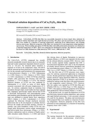
Figure 3. SEM images of CCTO thin films as a function of sintering temperature.
silicon based compounds. However, when the sintering
temperature was increased to 750°C, the second phases
disappeared and pure phase CCTO thin film was
obtained. The film exhibited (220) preferential orientation.
The diffraction patterns showed distinct (220), (400),
(422) and (440) peaks along with low intensity peaks.
The peaks match with the corresponding peaks in bulk
CCTO, revealing polycrystalline nature of the film with
cubic perovskite structure (space group, Im3) (Bochu
et al 1979). With further increase in sintering temperature
and sintering time, no major structural changes were
observed.
Representative SEM surface and lateral images
obtained for the CCTO films as a function of sintering
temperature is shown in figure 3. The SEM images sup-
port the XRD results revealing polycrystalline nature.
The film exhibited exaggerated grain growth and duplex
microstructure consisting of large grains in excess of
400 nm in length and small grains of < 200 nm. The
exaggerated grain growth may be attributed to the CuO
based liquid phase sintering (Leret et al 2007). Trapped
pores were observed in large grains and in grain bounda-
ries when the sintering temperature was above 900°C.
The pores may have developed from the abnormal grain
growth and the grain boundaries moving quickly during
the sintering process (Liu et al 2007). Due to the exa-
ggerated grain growth, any significant variation in grain
growth with sintering temperature was not observed. Lat-
eral view image in the figure corresponds to a three-time
spin coated film sintered at 800°C. The image indicates a
well densified structure with some columnar grains. The
average thickness of a three-time spin coated film was
~ 400 nm. The interface between the CCTO film and
bottom electrode was sharp implying negligible inter-
diffusion across the interface.
3.2 Dielectric properties
The variation of k and the dielectric loss recorded for the
films as a function of frequency of measurement is shown
in figure 4. The dielectric measurements were carried out
in four selected frequencies, viz. 1 kHz, 100 kHz,
500 kHz and 1 MHz. The CCTO film sintered at 750°C
showed a k value of ~ 2100 and a loss tangent of ~ 0⋅06 at
1 kHz. The decrease in k when sintering temperature was
above 900°C is associated with the trapped porosity as
observed by SEM. At higher measuring frequencies, k
decreased gradually, accompanied by a corresponding
increase in loss factor.
The large k at lower frequencies is suggested to be
associated with the Maxwell-Wagner contributions of
4. Viswanathan S Saji and Han Cheol Choe206
Figure 4. Dielectric constant and dielectric loss of CCTO thin film at different sintering temperatures
as a function of measuring frequency.
depletion layers at grain boundaries or interfaces between
the sample and contacts (Adams et al 2002; Lukenheimer
et al 2004). So far, the internal barrier layer capacitor
(IBLC) model has been widely accepted as the most
likely mechanism to elucidate the CDC in CCTO. The
difference of conductivity between grain boundary and
grain volume causes the charge accumulation on the grain
boundary on a mesoscopic scale, which results in large
quantity boundary barrier layer capacitors. On a macro-
scopic scale, the electrode contact effect may play a
significant role in CDC. Liu et al (2008) showed that
electrode and grain boundary act as two depletion layers
with distinct relaxation. On increasing the frequency, the
space charge polarization relaxes leading to decrease in k.
It has been shown that the frequency of dielectric relaxa-
tion was much lower in the case of CCTO film when
compared to that of the bulk ceramic (Shri Prakash et al
2008). The dielectric properties of the film obtained in
the present work is comparable with that reported for
polycrystalline CCTO thin films (Si et al 2002; Fang and
Shen 2003; Fang et al 2004; Shri Prakash et al 2008).
The high dielectric constant obtained for the CCTO film
in the present study indicates its possible application in
microelectronic devices.
4. Conclusions
Highly oriented CCTO thin films were successfully
deposited on boron doped silica substrate at a sintering
temperature of 750°C. Effect of sintering temperature on
the phase and microstructure of the film was investigated.
The film formed was polycrystalline in nature with (220)
preferential orientation. SEM microstructures of the films
revealed a bimodal size distribution of grains. Dielectric
constant and loss tangent at 1 kHz obtained for the film
sintered at 750°C was k ~ 2000 and tanδ ~ 0⋅05, respec-
tively.
Acknowledgement
The authors express their sincere gratitude to Professor
Yong Soo Cho, Department of Materials Science and
Engineering, Yonsei University, Korea.
5. Chemical solution deposition of CaCu3Ti4O12 thin film 207
References
Adams T B, Sinclair D C and West A R 2002 Adv. Mater. 14
1321
Adams T B, Sinclair D C and West A R 2006 Phys. Rev. B73
094124
Bochu B, Deschizeaux M N and Joubert J C 1979 J. Solid State
Chem. 29 291
Briźe V, Gruener G, Wolfman J, Fstyeyeva K, Tabellout M and
Gervais F 2006 Mater. Sci. Eng. B129 135
Chung S Y, Kim I L and Kang S J L 2004 Nat. Mater. 3 774
Cohen M H, Neaton J B, He L and Vanderbilt D 2003 J. Appl.
Phys. 94 3299
Fang L and Shen M 2003 Thin Solid Films 440 60
Fang L, Shen M and Cao W 2004 J. Appl. Phys. 95 6483
Feng L, Wang Y, Yan Y, Cao G and Jiao Z 2006 Appl. Surf.
Sci. 253 2268
Homes C C, Vogt T, Shapiro S M, Wakimoto S and Ramirez
A P 2001 Science 293 673
Jiménez R, Calzada M L, Bretos I, Goes J C and Sombra A S B
2007 J. Eur. Ceram. Soc. 27 3829
Leret P, Fernandez J F, de Frutos J and Fernandez-Hevia D
2007 J. Eur. Ceram. Soc. 27 3901
Liu L, Fan H, Fang P and Jin L 2007 Solid State Commun. 142
573
Liu L, Fan H, Wang L, Chen X and Fang P 2008 Philos. Mag.
88 537
Lu W, Feng L, Cao G and Jiao Z 2004 J. Mater. Sci. 39 3523
Lukenheimer P, Fichtl R, Ebbinghaus S G and Loidl A 2004
Phys. Rev. B70 172102.
Martin L, Guillemet-Fritsch S, Durand B, Levchenko A A,
Navrotsky A and Lebey T 2008 J. Am. Ceram. Soc. 91 485
Ramirez A P, Subramanian M A, Gardel M G, Blumberg G, Li
D, Vogt T and Shapiro S M 2000 Solid State Commun. 115 217
Schwartz R W 1997 Chem. Mater. 9 2325
Shri Prakash B, Varma K B R, Michau D and Maglione M 2008
Thin Solid Films 516 2874
Si W, Cruz E M, Johnson P D, Barnes P W, Woodward P and
Ramirez A P 2002 Appl. Phys. Lett. 81 2056
Subramanian M A, Li D, Duan N, Reisner B A and Sleight A W
2000 J. Solid State Chem. 151 323
Sun D L, Wu A Y and Yin S T 2008 J. Am. Ceram. Soc. 91 169