2. To develop integrated, simple to use SMT packaged Customer friendly parts
that eliminates complex and expensive chip Assembly and related
performance degradation.
IMS-2010
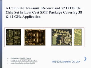
3. Laminate Package
Chip Scale Package High performance at frequencies from DC-mmW
Eliminates one assembly step of die attach and wire bonding as
complete package is processed with IC.
Virtually eliminates parasitic associated with plastic, lead frames
and bond wires & provides true air cavity
Enables ultra-thin IC substrates to dissipate heat and whole
package is thinner than current solutions so much better for
thermal dissipation for PAs.
Finished GaAsCap wafer can be RF probed as accurately as ‘on
wafer’ probing and so suitable for large scale manufacturing test
and does not need any PCB or custom test fixture/contactor board
for testing.
Estimated cost is $0.10/mm2) even at mmW frequencies.
Built to specifications, Uses Rogers 4350
material for base and lid
IMS-2010
5. IF1
IF2
Balun
Balun
RF
LO
Parameter Unit Spec.
LO Frequency GHz 17-23
IF Frequency GHz DC-5
Conversion Gain dB 10
Gain Dynamic
Range
dB 24
NF dBm 17/23
Input IP3 dBm +7/+16
LO Power dBm 20
2*LO Leakage dBc 10
S.B. Suppression dBc 15
RL dB 10
Current (5V) mA 300
Diesize:2.65x3x0.1mm
IMS-2010