1. Re-configurable High Speed Arithmetic Functions in a Non-Volatile FPGA
1
Rufino T. Olay III
Customer Engineer
ABSTRACT
Achieving 200 MHz multiplier data rates are easily attainable by placing the predetermined
multiplier values in RAM. This paper will explore the reconfigurablity of these multipliers and
other arithmetic functions in a Non-Volatile FPGA with embedded RAM.
INTRODUCTION
Arithmetic functions such as multipliers require many levels of logic, which have an
undesirable effect on system speed. Even with pipelining techniques, the speeds above
100MHz are hard to attain. By configuring a Dual Port RAM as a ROM, the predetermined
results of the multiplier can be loaded in one clock domain and read on another. This
technique does not require any pipelining and thereby provides the desired arithmetic output
on the next clock cycle. The three design techniques illustrated below will concentrate on
multipliers in RAM, but any arithmetic function, pattern generator or set of patterns, can be
used in its place.
Quicklogic’s QuickRAM family with its embedded RAM, routing rich architecture, and
abundant logic cells, provide an excellent platform for this type of implementation. The
technique of loading the predetermined arithmetic values into the RAM will allow the designer
to remove any gating factors associated with arithmetic functions.
FUNCTIONAL DESCRIPTION
SYSTEM LEVEL FUNCTIONALITY
The RAM in the QuickLogic QuickRAM family can be configured as a ROM, RAM or FIFO.
Two different approaches illustrate the techniques. The first method, “RAM loaded via
external EEPROM”, is the general approach to loading the RAM with the arithmetic values.
The second method, “RAM loaded via internal logic”, is a novel approach that allows the user
to load the RAM with dynamic arithmetic values.
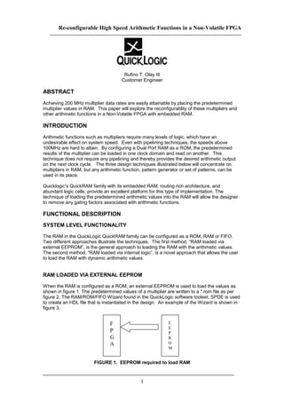
RAM LOADED VIA EXTERNAL EEPROM
When the RAM is configured as a ROM, an external EEPROM is used to load the values as
shown in figure 1. The predetermined values of a multiplier are written to a *.rom file as per
figure 2. The RAM/ROM/FIFO Wizard found in the QuickLogic software toolset, SPDE is used
to create an HDL file that is instantiated in the design. An example of the Wizard is shown in
figure 3.
FIGURE 1. EEPROM required to load RAM
F
P
G
A
E
E
P
R
O
M
2. Re-configurable High Speed Arithmetic Functions in a Non-Volatile FPGA
2
FIGURE 2. 4x4 Multiplier ROM File Example
// 4x4 ROM file example
rom=rom4x4
depth=256
width=8
asyncread=false
radix=binary
data
[0] = "00000000" // 4’h0 * 4’h0 = 8’h0;
.
.
[16] = "00000000" // 4’h0 * 4’hF = 8’h0;
[17] = "00000001" // 4’h1 * 4’h0 = 8’h1;
.
.
[255] = "11100001" // 4’hF * 4’hF = 8’hE1
end
FIGURE 3. RAM/ROM/FIFO Wizard
3. Re-configurable High Speed Arithmetic Functions in a Non-Volatile FPGA
3
RAM LOADED VIA INTERNAL LOGIC
The second method is utilized when designs require the ability to have variable high-speed
arithmetic functions, but the use of an external EEPROM is either not available or prohibited.
The design can be partitioned into two major systems as shown in figure 4.
FIGURE 4. Block diagram for internal initialization
The block on the left “Low speed ckt to load RAM w/ values” initializes the Dual Port RAM and
contains three building blocks:
- counter
- multiplier
- clock divider
Circuit that handles user configureable multiplier values
In DSP functions, such as FIR and IIR filters, a frame is multiplied by a constant coefficient.
The following circuit handles the case when the multiplier value needs to be reconfigureable,
such as during debug or field upgrades.
Figure 5. Specific Block Diagram 1 for initializing RAM with internal Logic
Low speed
ckt to load
RAM w/
values
R
A
M High
speed
Data
Low
speed
Data
counter
Multiplier value
Multiplicand
CLK
Address
Data
Address
Data
Frame
Data
R
A
M
Ready
4. Re-configurable High Speed Arithmetic Functions in a Non-Volatile FPGA
4
The high-speed clock is divided and then fed to the clock inputs of the multiplier and counter.
After the reset has been de-asserted, the counter will cycle through all the values. The
counter is used to represent all the input values of a multiplier. For instance, an 8-bit value
has 256 permutations.
The count values are used in two places:
- Address pointer for the RAM
- Multiplicands for the multiplier
The count values are sent to the multiplier as the multiplicands, and then multiplied with the
user-supplied multiplier value. The user-supplied multiplier value need be valid only for one
cycle and then latched. Table 1 shows the address value as a function of the counter output.
It also shows the constant multiplier value, 8 bit multiplicand value and result of the multiplier
User Entered
Multiplier Value
Counter Value
= Address
Pointer (8-bit
wide
Multiplicand)
Data
(Multiplier Output)
9 0 0
9 1 9
9 2 18
9 254 2286
9 255 2295
Table 1. Multiplier, Multiplicand, Resulting Output
The result 2295 translates to a 12-bit result. QuickLogic’s RAM blocks can be configured as:
- 64x18, 128x9, 256x4, 512x2
For this application 3 RAM blocks are concatenated to implement the above configuration as a
256x12 RAM block. To do this the RAM Wizard is employed to automatically create the
256x12 RAM. The output of the Wizard is an HDL, that is instantiated inside the top level
design.
The Ready signal is asserted upon the completion of the initialization of the RAM.
Figure 6. Creating a 256x12 RAM block from the RAM Wizard
5. Re-configurable High Speed Arithmetic Functions in a Non-Volatile FPGA
5
Circuit that handles constant multiplier values
In designs that do not require re-configurable multipliers but still require the high-speed
characteristics of a ROM, the configuration below is appropriate.
The design shown in figure 7 utilizes a counter and a multiplier to load the Dual Port RAM.
The counter width equals the total number of bits to be multiplied. For instance, a 4x4
multiplier would require an 8-bit counter. The counter is split in half. Bits [3:0] represent the
multiplier value and bits [7:4] represent the multiplicand.
As the counter sequences through the count values, each half of the counter bits are sent to
the multiplier. This same value is also used as the address pointer. See Table 2 for details.
After cycling through the count values the Ready signal is asserted to indicate the completion
of the initialization of the RAM.
Figure 7. Specific Block Diagram 2 for initializing RAM with internal Logic
counter
LSBs MSBs
CLK
Address
Data
Address
Data
Frame
Data
R
A
M
Ready
6. Re-configurable High Speed Arithmetic Functions in a Non-Volatile FPGA
6
MSB of counter LSB of counter Address Data
Multiplier Outputs
0 0 0 0
0 1 1 0
. . . .
0 15 15 0
1 0 16 0
1 1 17 1
. . . .
15 15 255 E1
Table 2. Counter Values, Address and Output Values
RESULTS
Below is a matrix that shows the different clock rates achievable for the various multiplier
types. By placing the arithmetic functions in RAM, performance was increased at least two
fold.
Multiplier Type Clock Rate (MHz) Speed Grade
4x4 (non piped) 87 -4
4x4 in RAM 200 -4
4’h9 * 8 bit
multiplicand
(non-piped)
95 -4
4’h9 * 8 bit in
RAM
200 -4
SUMMARY
As was shown, there are many different approaches to achieving very fast arithmetic
functions, three of which were proposed here. The predetermined output values of arithmetic
functions can be placed in RAM as a ROM. This provides the user with an extremely fast
arithmetic operation without pipelining. These techniques employ only a limited amount of
complementary logic, but garner the added value of a much faster sampling rate. Gating
factors concerning arithmetic operations are removed and are now replaced by 200 MHz, full
functional solutions.
![Re-configurable High Speed Arithmetic Functions in a Non-Volatile FPGA
2
FIGURE 2. 4x4 Multiplier ROM File Example
// 4x4 ROM file example
rom=rom4x4
depth=256
width=8
asyncread=false
radix=binary
data
[0] = "00000000" // 4’h0 * 4’h0 = 8’h0;
.
.
[16] = "00000000" // 4’h0 * 4’hF = 8’h0;
[17] = "00000001" // 4’h1 * 4’h0 = 8’h1;
.
.
[255] = "11100001" // 4’hF * 4’hF = 8’hE1
end
FIGURE 3. RAM/ROM/FIFO Wizard](data:image/gif;base64,R0lGODlhAQABAIAAAAAAAP///yH5BAEAAAAALAAAAAABAAEAAAIBRAA7)