An analytical method with numerical results to be used in the design of optic...
Poster_STEM_Research
1. Carbon Nanotube-Based Nanoelectronic Devices and Circuits
Xavier Crutcher, John Elike, Richard Hamnond, Joe’l Johnson, Jada Gray, Alishia Reynolds, and Meskerem Zergaw
M t D Zhi Xi d D S til i B d k
AAMU
Mentor: Dr. Zhigang Xiao and Dr. Satilmis Budak
Department of Electrical Engineering and Computer Science, Alabama A&M University
GOALS
1) To control the positioning and assembly of carbon
nanotubes using dielectropheresis technique.
2) To implement Sb2Te3 and Bi2Te2Se semiconductor
MOTIVATION AND SIGNIFICANCE The fabrication of CNTFETs has been the subject of extensive research, but challenges remain. One of the
major problems is the control of the positioning and assembly of carbon nanotubes. Another main obstacle is the low yield of well performing devices
because currently there is no effective way to separate metallic carbon nanotubes, which shunt FET characteristics, from semiconducting tubes, which
are the active elements of the device.
2) To implement Sb2Te3 and Bi2Te2Se semiconductor
materials as the source and drain contact material in
the fabrication of carbon nanotube field-effect
transistors (CNTFETs) in order to improve their
electrical properties such as drain-source current (IDS)
on/off ratio and saturation.
To circumvent these problems, in this work dielectrophoresis has been used for the deposition and alignment of tubes, while semiconducting electrodes
have been employed to selectively turn off metallic nanotubes. The reason for this substitution resides in the current-blocking action produced by the
back-to-back metal–semiconductor junctions formed at the interfaces between semiconducting electrodes and metallic nanotubes. This current-blocking
action electrically isolates metallic nanotubes and as a result improves the performance of the device.
This novel fabrication process has general meaning, and could be employed in future wafer-scale CNTFET-based nanoelectronic circuits with
semiconductor contact materials.
APPROACH
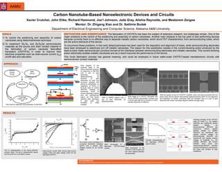
Fl di f th
SWCNT
powder
(3 mg)
NMP
(20 ml)
+
Dispersion
Ultrasonication (2
hrs)
Flow diagram of the
essential steps in the
device fabrication process.
(a) Alignment of SWCNTs
onto a pair of gold
electrodes via
dielectrophoresis. (b)
Removal of gold
electrodes by gold and
chromium etchants (PR
stands for photoresist). (c)
Deposition of Sb Te or
Centrifuge
(14000 rpm/30
min)
Flow chart for dispersion and purification of SWCNTs.
Deposition of Sb2Te3 or
Bi2Te2Se layer to contact
SWCNTs, followed by
photoresist lift-off to
remove deposited material
from the interelectrode
region. (d) Final device
obtained after deposition
of gate oxide and
formation of metal
contacts.
SEM of SWNTs aligned onto a
pair of gold electrodes via
dielectrophoresis.
SEM image of a CNTFET fabricated with
Sb2Te3-SWCNT source/drain contacts and
a narrow gate defined by focused ion beam
assisted deposited of platinum.
SEM micrograph of part of a CNTFET oscillator, which has been processed with one
photo mask and the electric field-directed dielectrophoresis (DEP) for the alignment
and deposition of carbon nanotubes (left) and enlarged view of a pair of gold
electrode with carbon nanotubes aligned between the gap (right).
RESULTS
Working principle of the CNTFET
valid for small VDS: (a) metallic
SWCNTs are channel-off without
applied voltage; (b)
semiconducting SWCNTs areg
channel-on without applied
positive voltage; (c) metallic
SWCNTs are channel-off with
applied positive voltage; (d)
semiconducting SWCNTs are
channel-off with applied positive
voltage. At moderate VDS, the
metallic SWCNTs still remain
blocked since while one
semiconductor/SWCNT Schottky
junction increases its conductance,
An inverter circuit consisting of a
p-channel field-effect transistor
(pFET) and a resistor (left);
diagram symbol for an inverter
SEM micrograph of a
fabricated CNTFET-based
inverter. SEM micrograph of the
Transfer characteristics of
the fabricated CNTFET-
based inverter.
The IV characteristics of the Sb2Te3-SWCNT
junction diode. The dot is measurement results
and the solid line is simulation results.
Drain-source current (IDS) versus drain-source
voltage (VDS) and gate voltage (VGS) for the
fabricated CNTFET.
the other one remains at high
impedance.
Acknowledgements
The authors thank National Science Foundation and Department of Homeland Security for financial support for this research.
(right).
inverter. g p
CNTFET in the inverter and
the CNTs aligned between
the electrodes.