Design and Implementation of VLSI Architecture for Image Scaling Processor
•
0 gefällt mir•640 views

In many Digital image processing applications, for processing of images or displaying the images on different size displays, they are use image scaling techniques in order to scale up/scale down of an image. In this paper, we are implement the 7 stage VLSI architecture at low cost with the edge oriented area-pixel scaling technique for achieve better image quality compared to other techniques. This method achieves better visual quality compared to previous methods. The seven-stage VLSI architecture of our image scaling processor yields a processing rate of about 200 MHz by using TSMC 0.18- m technology
![Design and Implementation of VLSI Architecture for Image Scaling Processor
| IJMER | ISSN: 2249–6645 | www.ijmer.com | Vol. 4 | Iss.9| Sept. 2014 | 27|
According to the required computations and memory space, we can divide the existing scaling methods
into two classes’ lower complexity and higher complexity scaling techniques. The complexity of the former is
very low and comparable to conventional bilinear method. The latter yields visually pleasing images by utilizing
more advanced scaling methods. In many practical real-time applications, the scaling process is included in end-user
equipment, so a good lower complexity scaling technique, which is simple and suitable for low-cost VLSI
implementation, is needed. In this project, to be consider the lower complexity scaling techniques only.
In this method area-pixel model is used instead of common point-pixel model. From the original image
it takes four pixels for calculating the one pixel of a scaled image. The modified area pixel scaling algorithm is
used in this method for obtain better edge preservation requires two times more of computations than the
bilinear method.
The main goal is to achieve low cost, for that edge-oriented area pixel scaling is used in this method. In
this design VLSI circuit is approximated and implemented at low cost.
II. Analysis of Image Scaling Technique
A. Area –Pixel Model
Instead of Common point model area pixel scaling technique performs scale-up/scale-down
transformation by taking each pixel is treated as one small rectangle but not a point. For example A source
image of 4 X 4 pixels is scaled up to the target image of 5 X 5 pixels. Obviously, the area of a target pixel is less
than that of a source pixel. the number of source pixels overlapped by the current target pixel window is one,
two, or a maximum of four. Let the luminance values of four source pixels overlapped by the window of current
target pixel at coordinate (k,l) be denoted as Fs(m,n), Fs(m+1,n), Fs(m,n+1) and Fs(m+1,n+1) and, respectively.
The estimated value of current target pixel denoted as can be calculated by weighted averaging the
luminance values of four source pixels with area coverage ratio as
Where W(m,n) ,W(m+1,n),W(m,n+1), and W(m+1,n+1) represent the weight factors of neighbouring source
pixels for the current target pixel at (k,l).Assume that the regions of four source pixels overlapped by current
target pixel window are denoted as A(m+1,n), A(m,n+1),and A(m+1,n+1),respectively, and the area of the
target pixel window is denoted as Asum..The weighted factors of four source pixels can be given as
Where Asum = A(m,n)+A(m+1,n)+ A(m,n+1)+A(m+1,n+1),
Let the width and height of the overlapped region Asum. be denoted as left(k,l)and top(k,l), and the width
and height of A(m+1,n+1) be denoted as right(k,l) and bottom(k,l). Then, the areas of overlapped regions can
be calculated by
[A(m,n),A(m+1,n), A(m,n+1),and A(m+1,n+1)] =
[left(k,l)xtop(k,l),right(k,l)xtop(k,l),left(k,l)bottom(k,l),right(k,l)bottom(k,l)]. (3)
The hardware implementation of area pixel model is very difficult at low cost. It requires many
manipulation operations like additions, multiplications, floating point operations to calculate one target pixel.
In order to reduce this computational complexity, we implement VLSI architecture to determine those
necessary coordinate values efficiently and quickly
We know that the direct implementation of area-pixel scaling requires some extensive floating-point
computations for the current target pixel at (k,l) to determine the four parameters, left (k,l),top (k,l),right (k,l) ,
and bottom (k,l). In the proposed process, we use an approximate technique suitable for low-cost VLSI
implementation to achieve that goal properly.
(1)
[W(m,n),W(m+1,n), ,W(m,n+1), ,W(m+1,n+1)] =
[A(m,n)/ Asum, A(m+1,n)/ Asum, A(m,n+1)/ Asum, A(m+1,n+1)/ Asum](2)] (2)
Where Asum = A(m,n)+A(m+1,n)+ A(m,n+1)+A(m+1,n+1)
[A(m,n),A(m+1,n),A(m,n+1),and A(m+1,n+1)] =
[left(k,l)xtop(k,l),right(k,l)xtop(k,l),left(k,l)bottom(k,l),right(k,l)bottom(k,l)]. (3)
We modify (3) and implement the calculation of areas of the overlapped regions as
[A’(m,n),A’(m+1,n),A’(m,n+1),A’(m+1,n+1)]](data:image/gif;base64,R0lGODlhAQABAIAAAAAAAP///yH5BAEAAAAALAAAAAABAAEAAAIBRAA7)
Empfohlen
Weitere ähnliche Inhalte
Was ist angesagt?
Was ist angesagt? (19)
Andere mochten auch
Andere mochten auch (20)
Ähnlich wie Design and Implementation of VLSI Architecture for Image Scaling Processor
Ähnlich wie Design and Implementation of VLSI Architecture for Image Scaling Processor (20)
Mehr von IJMER
Mehr von IJMER (20)
Kürzlich hochgeladen
Kürzlich hochgeladen (20)
Design and Implementation of VLSI Architecture for Image Scaling Processor
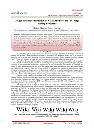
- 1. International OPEN ACCESS Journal Of Modern Engineering Research (IJMER) | IJMER | ISSN: 2249–6645 | www.ijmer.com | Vol. 4 | Iss.9| Sept. 2014 | 26| Design and Implementation of VLSI Architecture for Image Scaling Processor Bukya. Balaji1, Yarra. Naresh2 1Associate Professor,2Assistant professor/Gandhi Academy of technical Education/JNTUH/T.S/ INDIA. I. Introduction In computer graphics, image scaling is the process of resizing a digital image. Scaling is a non-trivial process that involves a trade-off between efficiency, smoothness and sharpness. As the size of an image is increased, so the pixels which comprise the image become increasingly visible, making the image appears "soft". Conversely, reducing an image will tend to enhance its smoothness and apparent sharpness. Apart from fitting a smaller display area, image size is most commonly decreased (or sub sampled or down sampled) in order to produce thumbnails. Enlarging an image (up sampling or interpolating) is generally common for making smaller imagery fit a bigger screen in full screen mode, for example. In “zooming” an image, it is not possible to discover any more information in the image than already exists, and image quality inevitably suffers. However, there are several methods of increasing the number of pixels that an image contains, which evens out the appearance of the original pixels.Pixel art scaling algorithms are image scaling algorithms specifically designed to up sample (enlarge) low-resolution pixel and line art that contains thin lines, solid areas of color rather than gradient fills or shading, and has not been anti-aliased. IMAGE scaling is widely used in many fields, ranging from consumer electronics to medical imaging. It is indispensable when the resolution of an image generated by a source device is different from the screen resolution of a target display. For example, we have to enlarge images to fit HDTV or to scale them down to fit the mini-size portable LCD panel. The most simple and widely used scaling methods are the nearest neighbour and bilinear techniques. An image size can be changed in several ways. The Fig 1(a) is Consider to doubling the size, The easiest way of doubling its size is nearest-neighbor interpolation, replacing every pixel with four pixels of the same color in Fig 1(b). The resulting image is larger than the original, and preserves all the original detail, but has undesirable jaggedness. The diagonal lines of the W, for example, now show the characteristic "stairway" shape. Other scaling methods are better at preserving smooth contours in the image. For example, bilinear interpolation produces the result in Fig 1(c).Linear (or bilinear, in two dimensions) interpolation is typically better than the nearest-neighbor system for changing the size of an image, but causes some undesirable softening of details and can still be somewhat jagged. Better scaling methods include bi cubic interpolation in Fig 1(d).For magnifying computer graphics with low resolution and/or few colors (usually from 2 to 256 colors) the best results will be achieved by hqx or other pixel art scaling algorithms. These produce sharp edges and maintain high level of detail. hq2x is in Fig 1(e). For scaling photos (and raster images with lots of colors) see also anti- aliasing algorithms called super sampling. (a) (b) (c) (d) (e) Fig 1: Different Scaled Images (a) Original image (b) Nearest-neighbor interpolation (c) Linear Interpolation (d) bi cubic (e) hq2x Abstract: In many Digital image processing applications, for processing of images or displaying the images on different size displays, they are use image scaling techniques in order to scale up/scale down of an image. In this paper, we are implement the 7 stage VLSI architecture at low cost with the edge oriented area-pixel scaling technique for achieve better image quality compared to other techniques. This method achieves better visual quality compared to previous methods. The seven-stage VLSI architecture of our image scaling processor yields a processing rate of about 200 MHz by using TSMC 0.18- m technology.
- 2. Design and Implementation of VLSI Architecture for Image Scaling Processor | IJMER | ISSN: 2249–6645 | www.ijmer.com | Vol. 4 | Iss.9| Sept. 2014 | 27| According to the required computations and memory space, we can divide the existing scaling methods into two classes’ lower complexity and higher complexity scaling techniques. The complexity of the former is very low and comparable to conventional bilinear method. The latter yields visually pleasing images by utilizing more advanced scaling methods. In many practical real-time applications, the scaling process is included in end-user equipment, so a good lower complexity scaling technique, which is simple and suitable for low-cost VLSI implementation, is needed. In this project, to be consider the lower complexity scaling techniques only. In this method area-pixel model is used instead of common point-pixel model. From the original image it takes four pixels for calculating the one pixel of a scaled image. The modified area pixel scaling algorithm is used in this method for obtain better edge preservation requires two times more of computations than the bilinear method. The main goal is to achieve low cost, for that edge-oriented area pixel scaling is used in this method. In this design VLSI circuit is approximated and implemented at low cost. II. Analysis of Image Scaling Technique A. Area –Pixel Model Instead of Common point model area pixel scaling technique performs scale-up/scale-down transformation by taking each pixel is treated as one small rectangle but not a point. For example A source image of 4 X 4 pixels is scaled up to the target image of 5 X 5 pixels. Obviously, the area of a target pixel is less than that of a source pixel. the number of source pixels overlapped by the current target pixel window is one, two, or a maximum of four. Let the luminance values of four source pixels overlapped by the window of current target pixel at coordinate (k,l) be denoted as Fs(m,n), Fs(m+1,n), Fs(m,n+1) and Fs(m+1,n+1) and, respectively. The estimated value of current target pixel denoted as can be calculated by weighted averaging the luminance values of four source pixels with area coverage ratio as Where W(m,n) ,W(m+1,n),W(m,n+1), and W(m+1,n+1) represent the weight factors of neighbouring source pixels for the current target pixel at (k,l).Assume that the regions of four source pixels overlapped by current target pixel window are denoted as A(m+1,n), A(m,n+1),and A(m+1,n+1),respectively, and the area of the target pixel window is denoted as Asum..The weighted factors of four source pixels can be given as Where Asum = A(m,n)+A(m+1,n)+ A(m,n+1)+A(m+1,n+1), Let the width and height of the overlapped region Asum. be denoted as left(k,l)and top(k,l), and the width and height of A(m+1,n+1) be denoted as right(k,l) and bottom(k,l). Then, the areas of overlapped regions can be calculated by [A(m,n),A(m+1,n), A(m,n+1),and A(m+1,n+1)] = [left(k,l)xtop(k,l),right(k,l)xtop(k,l),left(k,l)bottom(k,l),right(k,l)bottom(k,l)]. (3) The hardware implementation of area pixel model is very difficult at low cost. It requires many manipulation operations like additions, multiplications, floating point operations to calculate one target pixel. In order to reduce this computational complexity, we implement VLSI architecture to determine those necessary coordinate values efficiently and quickly We know that the direct implementation of area-pixel scaling requires some extensive floating-point computations for the current target pixel at (k,l) to determine the four parameters, left (k,l),top (k,l),right (k,l) , and bottom (k,l). In the proposed process, we use an approximate technique suitable for low-cost VLSI implementation to achieve that goal properly. (1) [W(m,n),W(m+1,n), ,W(m,n+1), ,W(m+1,n+1)] = [A(m,n)/ Asum, A(m+1,n)/ Asum, A(m,n+1)/ Asum, A(m+1,n+1)/ Asum](2)] (2) Where Asum = A(m,n)+A(m+1,n)+ A(m,n+1)+A(m+1,n+1) [A(m,n),A(m+1,n),A(m,n+1),and A(m+1,n+1)] = [left(k,l)xtop(k,l),right(k,l)xtop(k,l),left(k,l)bottom(k,l),right(k,l)bottom(k,l)]. (3) We modify (3) and implement the calculation of areas of the overlapped regions as [A’(m,n),A’(m+1,n),A’(m,n+1),A’(m+1,n+1)]
- 3. Design and Implementation of VLSI Architecture for Image Scaling Processor | IJMER | ISSN: 2249–6645 | www.ijmer.com | Vol. 4 | Iss.9| Sept. 2014 | 28| =[left’(k,l) x top’(k.,l),right’(k,l) x top’(k,l), left’(k,l) x bottom’ (k, l), right’ (k, l) x bottom’ (k, l)]. (4) Those left’ (k, l),top’ (k.,l),right’(k,l) and bottom’ (k, l) are all 6-b integers and given as [left’ (k,l), top’ (k,l),right’ (k,l) , bottom’ (k,l)]= Appr[left(k,l),top (k,l),right (k,l) , bottom (k,l)] (5) Where Appr represents the approximate operator adopted in this design and will be explained in detail later. To obtain better visual quality, a simple low-cost edge catching technique is employed to preserve the edge features effectively by taking into account the local characteristic existed in those available source pixels around the target pixel. The final areas of the overlapped regions are given as [A”(m.n),A”(m+1,n),A”(m,n+1),A”(m+1,n+1)] = ([ A’(m.n),A’(m+1,n),A’(m,n+1),A’(m+1,n+1)]) (6) Where we adopt a tuning operator to tune the areas of four overlapped regions according to the edge features obtained by edge-catching technique. By applying (6) to (1) and (2), we can determine the estimated luminance value of the current target pixel. Then we describe the low-cost edge-catching technique in detail. III. VLSI Architechture for Edge- Oriented Image Scaling Fig 2: Block diagram of VLSI architecture for Edge oriented Area Pixel scaling Method. Edge oriented Area Pixel scaling method requires low computational complexity and only one line memory buffer, so it is suitable for low-cost VLSI implementation. Fig.2 shows block diagram of the seven- stage VLSI architecture for this scaling method. The architecture consists of seven main blocks: approximate module (AM), register bank (RB), area generator (AG), edge catcher (EC), area tuner (AT), target generator (TG), and the controller. Each of them is described briefly in the following subsections. A Approximate Module When a source image of SW X SH pixels is scaled up or down to the target image OF TW X TH pixels, the AM generates left(k,l),top(k,l),right(k,l),bottom(k,l), respectively, for each target pixel from left to right and from top to bottom. In this VLSI implementation n is set to 3, so each rectangular target pixel is treated as 23 x 23 uniform-sized grids. It is composed two stage pipelined architecture. B Register Bank In this design, the estimated value of the current target pixel is calculated by using the luminance values of 2 x 4 neighbour ing sour ce pixel s Fs(m-1,n),Fs (m,n),Fs(m+1,n), Fs(m+2,n), Fs(m- 1,n+1), Fs(m,n+1), Fs(m+1,n+1,),and Fs(m+2,n+1). The register bank, consisting of eight registers, is used to provide those source luminance values at exact time for the estimated process of current target pixel. the
- 4. Design and Implementation of VLSI Architecture for Image Scaling Processor | IJMER | ISSN: 2249–6645 | www.ijmer.com | Vol. 4 | Iss.9| Sept. 2014 | 29| line buffer is used to store the pixel values of one row in the source image. It has totally eight registers. When the controller enables the shift operation in RB, two new values are read into RB (Reg3 and Reg7) and the rest 6-pixel values are shifted to their right registers one by one. The 8-pixel values stored in RB will be used by EC for edge catching and by TG for target pixel estimating. C Area Generator For each target pixel ,AG calculates the areas of the overlapped regions A’(m,n),A’(m+1,n),and A’(m+1,n+1).the architecture of area generator consists of pipeline register and 4 x 4 integer multipliers. D Edge catcher Fig. 3: Architecture of edge catcher E Area Tuner AT is used to modify the areas of the four overlapped regions based on the current local edge information ( and U GE provided by EC). Fig.4 shows the two-stage pipeline architecture of AT. If U GE is equal to 1, the upper row (row ) in current pixel window is more important. On the contrary, if U-GE is equal to 0, the lower row (row n+1) is more important. finally ,the tuned areas A’’(m,n),A’’(m+1,n),A’’(m,n+1) and A’’(m+1,n+1) are sent to TG. Fig.4: Architecture of area tuner
- 5. Design and Implementation of VLSI Architecture for Image Scaling Processor | IJMER | ISSN: 2249–6645 | www.ijmer.com | Vol. 4 | Iss.9| Sept. 2014 | 30| EC implements the proposed low-cost edge-catching technique and outputs the evaluating parameter LA, which represents the local edge characteristic of current pixel at coordinate. Fig.3 shows the architecture of EC where SUB unit generates the difference of two inputs and lSUBl unit generates the two inputs’ absolute value of difference. The comparator CMP outputs logic 1 if the input value is greater than or equal to Winh/2. The binary compared result, denoted as U_GE, is used to decide whether the upper row (row n) in current pixel window is more important than the lower row (row n+1) in regards to catch edge features. F Target Generator By weighted averaging the luminance values of four source pixels with tuned-area coverage ratio ,TG implements and determines the F^T(k,l).Fig.5 shows the shows the two-stage pipe line architecture of TG. Four MULT units and three ADD units are used . Fig.5 Architecture of target generator G CONTROLLER The controller, realized with a finite-state machine, monitors the data flow and sends proper control signals to all other components. In the design, AM, AT, and TG require two clock cycles to complete their functions, respectively. Both AG and EC need one clock cycle to finish their tasks, and they work in parallel because no data dependency between them exists. For each target pixel, seven clock cycles are needed to output the estimated value F^T(k,l). IV. Result Analysis To reduce hardware cost, we adopt the low-cost technique suitable for VLSI implementation to perform area-pixel scaling. To verify the computational complexity, the scaling method is implemented in VHDL language on the 2.8-GHz Pentium 4 processor with 512-MB memory and the 520-MHz INTEL XScale PXA270 with 64-MB memory, respectively. Table 6.1 shows the computing time (in the unit of second) of enlarging image from the size of 352 x 288 to the size of 300 x 200 for the two processors. Obviously, this method requires less computing time than previous method, and previous method needs much longer time due to extensive computations. To explore the performance of quantitative evaluation for image enlargement and reduction, first we scale the twelve 352 x 288 test images to the size of 400 x300, and 300 x 200, respectively, by using this method. .Here, the output images of Edge- Oriented image scaling method are generated by the proposed VLSI circuit after post-layout transistor-level simulation. The output images of other scaling methods are all generated with software C programs. Simulation results show that this design achieves better quantitative quality than the previous low-complexity scaling methods. A Simulation Results: The below Fig.6 shows the simulation results of the Scaled down image. Various signals involved in the simulation of the Scaled down image are Input Signals: blue, green, image_scaleion, imgcolumns, imglines, red, clk, image scaled image, Mono, processRGB, reset Output Signals: processingRGB, image_scaleing, addr, din,we
- 6. Design and Implementation of VLSI Architecture for Image Scaling Processor | IJMER | ISSN: 2249–6645 | www.ijmer.com | Vol. 4 | Iss.9| Sept. 2014 | 31| Fig.6: Simulation results of Scaled down Image The below Fig.7 shows the simulation results of the Scaled up image. Various signals involved in the simulation of the Scaled up image are Input Signals: blue, green, image_scaleion, imgcolumns, imglines, red, clk, image_scaledimage, Mono, processRGB, reset Output Signals: processingRGB, image_scaleing, addr, din, we Fig.7 Simulation results of Scaled up Image
- 7. Design and Implementation of VLSI Architecture for Image Scaling Processor | IJMER | ISSN: 2249–6645 | www.ijmer.com | Vol. 4 | Iss.9| Sept. 2014 | 32| B RTL (Register Transfer Level) Schematic View Fig.8 RTL (Register Transfer Level) View Observations: The above Fig.8 Shows RTL view, which displays the top level Schematic symbol for the design. It is the integration of all sub modules as a whole. RTL view gives the various design elements and connectivity between them. C Input and Output Images: (a) Input Images Fig.9 Input images (a) Fruits image of 352 x 288 pixels (b) Building image of 352 x 288 pixels To achieve the goal of low cost, the edge oriented area-pixel scaling technique is implemented with low-complexity VLSI architecture in this design. Here we apply images of size 352x288 as an input. (b) Output images:
- 8. Design and Implementation of VLSI Architecture for Image Scaling Processor | IJMER | ISSN: 2249–6645 | www.ijmer.com | Vol. 4 | Iss.9| Sept. 2014 | 33| Scaled down images: The proposed architecture is edge oriented image scaling technique. It is adopted to preserve the image edge features effectively so as to achieve better image quality. Here we get scaled down images of size 300x200 as for requirement by using this technique. Fig.10 Output Scaled Down images (a) Fruits image of 300 x 200 pixels (b) Building image of 300 x 200 pixels Scaled up images: (a) (b) Fig.11 Output Scaled up images (a) Fruits image of 400 x 300 pixels (b) Building image of 400 x 300 pixels V. Conclusion A low-cost image scaling process is proposed in this project. The experimental results demonstrate that our design achieves low computational complexity and only one line memory buffer, so it is suitable for low- cost better performances in both objective and subjective image quality than other low-complexity scaling methods. This scaling method requires VLSI implementation.Furthermore; an efficient VLSI architecture for the proposed method is presented. In this simulation, this project simulation is operates with a clock period of 5 ns and achieves a processing rate of 200 mega pixels/second. The architecture works with monochromatic images, RGB colour images easily. Finally it is implemented the image scaled up in 352x288 to 400x300 and scaled down in 352x288 to 300x200,and without effecting the input image. The output results show that our design achieves better quantitative quality than the previous low-complexity scaling methods. The simple edge catching technique is adopted to preserve the image edge features effectively, so it achieved better image quality.
- 9. Design and Implementation of VLSI Architecture for Image Scaling Processor | IJMER | ISSN: 2249–6645 | www.ijmer.com | Vol. 4 | Iss.9| Sept. 2014 | 34| REFERENCES [1] C. Kim, S. M. Seong, J. A. Lee, and L. S. Kim, “Winscale: An image scaling algorithm using an area pixel model,” IEEE Trans. Circuits Syst. Video Technol., vol. 13, no. 6, pp. 549–553, Jun. 2003. [2] I. Andreadis and A. Amanatiadis, “Digital image scaling,” in Proc.IEEE Instrum. Meas. Technol. Conf.,May 2005, vol. 3, pp. 2028–2032. [3] H. A. Aly and E. Dubois, “Image up-sampling using total-variation regularization with a new observation model,” IEEE Trans. Image Process., vol. 14, no. 10, pp. 1647–1659, Oct. 2005. [4] K. Ramchandran, A. Ortega, K. Metin Uz, and M. Vetterli, “Multiresolution broadcast fordigital HDTV using joint source/channel coding.” IEEE Journal on Selected Areas in Communications, 11(1):6−23, January 1993. [5] R. C. Gonzalez and R. E.Woods, Digital Image Processing. Reading,MA: Addison-Wesley, 1992. [6] W. K. Pratt, Digital Image Processing. New York: Wiley-Interscience,1991. [7] T. M. Lehmann, C. Gonner, and K. Spitzer, “Survey: Interpolation methods in medical image processing,” IEEE Trans. Med. Imag., vol.18, no. 11, pp. 1049–1075, Nov. 1999. [8] C.Weerasnghe, M. Nilsson, S. Lichman, and I. Kharitonenko, “Digital zoom camera with image sharpening and suppression,” IEEE Trans.Consumer Electron., vol. 50, no. 3, pp. 777–786, Aug. 2004. [9] S. Fifman, “Digital rectification of ERTS multispectral imagery,” in Proc. Significant Results Obtained from Earth Resources Technology Satellite-1, 1973, vol. 1, pp. 1131–1142. [10] J. A. Parker, R. V. Kenyon, and D. E. Troxel, “Comparison of interpolation methods for image resampling,” IEEE Trans. Med. Imag., vol.MI-2, no. 3, pp. 31–39, Sep. 1983. BIOGRAPHIES B.Balaji received the B.Tech degree in Electronics & Communication Engineering from JBIET college in JNTU Hyderabad and his Masters degree from NCET College-Kakinada in 2003 and 2009 respectively. He is currently working as Associate Professor in Gandhi Academy of Technical Education His interests are Imag processing, VLSI Chip design,etc. Yarra.Naresh received the B.Tech degree in Electronics & Communication Engineering and his Masters degree from Anurag Engineering college in JNTU Hyderabad in 2008 and 2011 respectively. He is currently working as Assistant Professor in Gandhi Academy of Technical Education His interests are Imag processing, VLSI Chip design,etc. .