1. Intersubband Absorption in InAlN/GaN Superlattices
Amanda M. Landcastle, Colin Edmunds, Oana Malis
Department of Physics
By growing a superlattice of alternating Indium Aluminum Nitride (InAlN) and Gallium
Nitride (GaN) layers, the quantum properties of the structure are used to achieve
energy transitions that cannot be accessed with typical semiconducting materials,
reaching the previously inaccessible 1.5-3.0 μm range. By utilizing the energy gap
difference of the two materials, a conduction band offset (CBO) arises, forming a
quantum well with quantized energy levels obeying the fundamental laws of quantum
mechanics. The InAlN is the barrier material while the GaN is the well material. The
width of the quantum well can be varied by changing the thickness of the GaN layer,
which allows the energy transitions in the well to be tailored to the goals of the
research. These transitions are known as intersubband transitions, occurring in the
energy levels of the CBO as opposed interband transitions which occur between the
energy levels in the conduction band to the valence band. The intersubband
transitions are made more likely to occur by δ-doping with silicon to push the Fermi
level closer to the conduction band which allows for easier excitations of the electrons
into the CBO to undergo the intersubband transitions. Fourier Transform Infrared
Spectroscopy is used to measure the optical properties of the superlattice. Several
geometries and measurement techniques are used to obtain spectra which can be
analyzed to further the progress of the research.
Abstract
What are semiconductors, and why are they important?
𝑓 𝐸 =
1
𝑒
(𝐸−𝐸 𝑓)
𝑘𝑇 + 1
Fermi function predicts the probability
of an electron existing above the Fermi
Level when T is above zero kelvin.
The valence band is filled with electrons while the conduction band is empty. In a
conductor, the electrons are free to move between the valence and conduction band.
An insulator’s valence and conduction bands have a large energy gap. With the Fermi
level located an equidistance from the two bands, the energy required for an electron
to make it past the Fermi level is too high for conduction to occur.
A semiconductor’s energy gap is smaller than an insulator’s, allowing for more
conducting electrons via thermal population, but not enough for use in advanced
technological devices.
The Fermi Level is the level
at absolute zero which the
electrons cannot be excited
past. The probability of
electrons able to be excited
past the Fermi level is
determined by the Fermi
function, which is dependent
on temperature.
Doping a semiconductor means that you add
impurities to the material in order to change the
location of the Fermi level in relation to either the
conduction band or the valence band.
We use n-type doping, which increases the
conductivity of the intrinsic semiconductor by adding
electron energy levels near the conduction band.
The electrons in these energy levels can be easily
excited into the conduction band.
δ-Doping
InAlN and GaN are both intrinsic semiconductors
with different bang gaps.
The purpose of doping the InAlN/GaN superlattice is to make the excitation of
electrons into the conduction band offset more probable.
A semiconductor is δ-doped if it is grown with Molecular Beam Epitaxy and the
doped layer is smaller than the de Broglie wavelength of the electrons.
400 600 800 1000 1200
-0.1
0.0
0.1
0.2
0.3
0.4
0.5
4.4 nm QWs
3 nm QWs
2.2 nm QWs
Absorption(arb.units)
energy (meV)
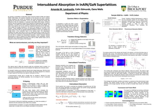
Transition Energy Selection
The graph to the right is a plot of transition
energies observed as the well thickness is
varied. As the well layer is grown thicker, the
transition energy associated with the nth energy
level decreases, by a factor of ~
1
𝐿2.
Using the infinite potential well is a good approximation for the transition energies
observed.
This is the familiar infinite square well equation for energy levels.
𝐸𝑙 ∶ energy which depends on the shape of the band
𝑚∗ ∶ effective mass
𝐿 ∶ width of the well
n: quantum number of energy level
𝐸𝑙 =
ћ2
𝜋2
𝑛2
2𝑚∗ 𝐿2
Quantum Wells in Superlattice
A superlattice of InAlN and GaN is grown.
Since they have different band gap energies,
a conduction band offset (CBO) is formed. A
quantum well comes about in the CBO, and
the quantized energy levels allow for
transitions of electrons which are inaccessible
in typical semiconducting materials.
Fermi’s golden rule is used to calculate the probability of transitions per unit time
from one energy eigenstate of a quantum system into another energy eigenstate
due to a perturbation, which is the incident light.
The system begins in an eigenstate ∣ 𝑖⟩ of a given Hamiltonian to a final state ∣ 𝑓⟩,
where the initial state is the ground state and the final state is the excited state.
Intersubband Transitions
Interband transitions occur between the
conduction and valence bands, so the
transition energy is determined by the
material properties.
Electrons are either thermally excited or optically pumped to the bottom of the
conduction band and are then excited into the conduction band offset where
they interact with the intersubband transitions.
Intersubband transitions occur in the
quantized energy levels of the quantum
well, allowing access to energies that
are not dependent on the band gap
energy of the material.
Intersubband Absorption
Fermi’s Golden Rule – rate of absorption
𝛼 = ћ𝜔
𝑊𝑎𝑏𝑠
𝑃
𝑁𝑢𝑚𝑏𝑒𝑟 𝑜𝑓 𝑝ℎ𝑜𝑡𝑜𝑛𝑠 𝑎𝑏𝑠𝑜𝑟𝑏𝑒𝑑 𝑝𝑒𝑟 𝑠𝑒𝑐𝑜𝑛𝑑 𝑝𝑒𝑟 𝑢𝑛𝑖𝑡 𝑣𝑜𝑙𝑢𝑚𝑒
𝑁𝑢𝑚𝑏𝑒𝑟 𝑜𝑓 𝑖𝑛𝑗𝑒𝑐𝑡𝑒𝑑 𝑝ℎ𝑜𝑡𝑜𝑛𝑠 𝑝𝑒𝑟 𝑠𝑒𝑐𝑜𝑛𝑑 𝑝𝑒𝑟 𝑢𝑛𝑖𝑡 𝑎𝑟𝑒𝑎
P is the optical intensity in
𝑊
𝑐𝑚2
Absorption coefficient
• Purdue University Department of Physics
• Dr. Oana Malis, Purdue University
• Colin Edmunds, Purdue University
• National Science Foundation (NSF)
• The College at Brockport: State University
of New York
Acknowledgements
Sample 052813a – InAlN – 14.8% Indium
Fourier Transform Infrared Spectroscopy is used to
find the absorption spectra for the sample. Direct
absorption measurement is used first. Photoinduced
absorption is used when electrons need to be
optically pumped in order to make more
intersubband transitions. This increases the
absorption.
Growth Scheme
Direct Absorption Method
No Gaussian or Lorentzian peak is
seen in either spectra, so no
absorption is observed.
Photoinduced Absorption Method
The doping scheme for this sample was thought to be optimal, so the fact that there was no
absorption was curious. The sample was mounted to indium film in the attempt to shift the
electromagnetic interference wave to be maximum at the quantum well surface. A simulation
of this concept is illustrated below.
The incident light undergoes total internal reflection within the sample. This leads to light
bouncing off the sides and interfering with itself. These interferences cause the ripples in the
image above. When the light waves interfere, a maximum is formed when constructive
interference occurs. Mounting the sample to indium should work because the complex index
of refraction for indium with the 2μm wavelength we are using is
ñ 2𝜇𝑚 = 2.97 + 14.5𝑖
This changes the boundary conditions and leads to a maximum at the semiconductor-metal
interface. This method worked, as seen in the spectrum above. There was absorption
observed at the energy expected. We were not able to recreate these results, but it shows
promise.
Conclusions and Future Work
The reason for InAlN/GaN not working is attributed
to inhomogeneities, referred to as InAlN nanorods,
embedded in the barrier materials of the
superlattice. This shows that the charge density
becomes localized in the nanorod, while the
superlattice remains relatively depleted. A high
charge density is needed for absorption.