PB FM 1990-2009 - Modeling Digital System Interconnections Using Time Domain Reflectometry Measurements
•
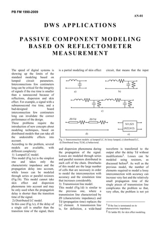
0 gefällt mir•209 views

![PB 1990-2009
[mrho] (DWS Waveform Viewer). This
40 A C methodology is also usable after
20 D the prototyping phase in order to
verify the behavior of the
S11 0 E prototype in all the situations by
replacing the pre-layout models
-20
B (with lumped or distributed
-40 parameters) with the measure-
based models. As a consequence it
0 10 20 30 40 50 60 70 80 90 100 is possible to use the simulation
TIME[nS] tool for investigating the signal
Fig. 2: Measured TDR response of the parameter S11 for a coaxial cable waveform where it is not possible
to measure it, for example inside
solvable with conventional SPICE- simulations a high degree of the package.
derived simulators. realism. Standard component
The DWS simulation engine, not libraries are already available, and
only allows designers to simulate the user can easily create new
the models already presented, but models with the utilities offered by
also, thanks to a new the graphic environment DWV
methodology, allows them to
use both standard models [mrho]
and behavioral descriptions 40
3
based on REFLECTOMETER 20
4
5
MEASUREMENTS in time 6
S11 7
0
domain (BTM - Behavioral Time 2
Modeling). -20
Using a reflectometer (TDR - -40 1
Time Domain Reflectometer) it is
possible to make a wide-band 0 10 20 30 40 50 60 70 80 90 100
TIME[nS]
characterization of one or two a)
port3 devices by means of the [rho] 1.0
4 7
measure of their scattering 5 6
0.8
parameters S11, S22, S21 e S12. 3
0.6
These models are very useful
S21
where sections of interconnection, 0.4
pieces of coaxial cable, packages,
0.2
etc. can be characterized 2
experimentally. Usually, an 0.0 1
accurate electrical modeling of 10 12 14 16 18 20 22 24 26 28 30
TIME[nS]
passive devices is not possible, b)
because of their complicated Fig. 3: Measure and PWL extraction of the S11(a) and S21(b).
* Coaxial cable: TDR and TDT simulation for model validation
*
******************************************************************
geometries. The utilization of field *
*
* Coaxial cable description using S-parameters with PWL extraction
simulators for the extraction of the *
BCOAX 20 0 30 0 S11=PWL ( 0.0NS -3.26e-02 18.6NS -1.99e-03 19.2NS 3.23e-02
parameters of the cross section + 20.4NS 2.49e-02 25.8NS 1.7e-02 47.2NS 8.42e-03 96.6NS 2.5e-03) Z0=50 TD=0
+ S21=PWL ( 0.0NS -1.53e-03 0.2NS 1.33e-01 .44NS 6.6e-01 .64NS 8.19e-01
shows a lot of troubles (first of all + 1.12NS 8.99e-01 2.2NS 9.42e-01 17.6NS 9.975e-01) Z0=50 TD=9.15NS
*
the input description) and can't *
* termination resistor
*
take into account the RLOAD 30 0 50
*
discontinuities that sometimes are *
*
* TDR step generator: a 2V step shows the result equivalent in RHO scale.
present along the device (for *
VTDR 20 0 PWL ( 0.0PS 0.0 3.25NS 0.0 3.28NS 2 ) 50
*
example connectors). The *
* analysis
measures are directly utilizable *
.TRAN TSTEP=30P TSTOP=100N A(VTDR, 20) V(30) LIMPTS=1000
.END
by the simulator giving the
Fig. 4: Simulation file (DWS syntax) used for model validation.
3Models with more than two ports will be
soon available.](data:image/gif;base64,R0lGODlhAQABAIAAAAAAAP///yH5BAEAAAAALAAAAAABAAEAAAIBRAA7)
Empfohlen
Weitere ähnliche Inhalte
Was ist angesagt?
Was ist angesagt? (19)
Andere mochten auch
Andere mochten auch (7)
Ähnlich wie PB FM 1990-2009 - Modeling Digital System Interconnections Using Time Domain Reflectometry Measurements
Ähnlich wie PB FM 1990-2009 - Modeling Digital System Interconnections Using Time Domain Reflectometry Measurements (20)
Mehr von Piero Belforte
Mehr von Piero Belforte (20)
Kürzlich hochgeladen
Kürzlich hochgeladen (20)
PB FM 1990-2009 - Modeling Digital System Interconnections Using Time Domain Reflectometry Measurements
- 1. PB FM 1990-2009 AN-01 DWS APPLICATIONS PASSIVE COMPONENT MODELING BASED ON REFLECTOMETER MEASUREMENT The speed of digital systems is is a partial modeling of skin effect circuit, that means that the input showing up the limits of the standard modeling based on lumped circuit parameters. Interconnections few centimeters long can be critical for the integrity of signals if the rise time is smaller a) b) than a nanosecond because of reflections, dispersion and skin effect. For example, a signal with a subnanosecond rise time, and a bad-designed board c) interconnection few centimeters long can invalidate the correct performance of the design. Z0 Td Z0 Td These problems require the S11,S21 introduction of new concepts about (S22,S12) modeling techniques, based on distributed models that can take all d) e) the undesirable effects into account. Fig. 1: Interconnection models: a) lumped LC, b) lossy lumped, c) distributed LC, d) Distributed lossy TLM, e) behavioral. According to the problem, several models are available, with and dispersion phenomena during waveform is transferred to the different complexity: the propagation of the signal. output after the delay Td without 1) Lumped LC model. Losses are modeled through series modifications1. Losses can be This model (Fig.1a) is the simplest and parallel resistors distributed in modeled using resistors, as one and takes only the each cell of the chain. Drawbacks discussed before2. As well as the characteristic impedance and the of this model are the large number previous model, the number of propagation delay into account, of cells that are necessary in order elements required to model a lossy while losses can be modeled to model the interconnection with interconnection with accuracy can through series or parallel resistors accuracy and the simulation time increase very fast and the relatively (Fig.1b). This model cannot take that increases considerably. small propagation time of the skin effect and dispersion 3) Transmission line model. single pieces of transmission line phenomena into account and may This model (Fig.1d) is similar to complicates the problem so that, be only used when the propagation the previous one, where a very often, the problem is not yet delay is shorter than the transition transmission line characterized by time of the signal. Z0 (characteristic impedance) and 2) Distributed LC model. Td (propagation time) replaces the In this case (Fig.1c), if the delay of LC element. A transmission line 1 If the line is terminated on its a single cell is smaller than the is, for definition, a wide-band characteristic impedance. transition time of the signal, there 2 Or ladder RL for skin effect modeling.
- 2. PB 1990-2009 [mrho] (DWS Waveform Viewer). This 40 A C methodology is also usable after 20 D the prototyping phase in order to verify the behavior of the S11 0 E prototype in all the situations by replacing the pre-layout models -20 B (with lumped or distributed -40 parameters) with the measure- based models. As a consequence it 0 10 20 30 40 50 60 70 80 90 100 is possible to use the simulation TIME[nS] tool for investigating the signal Fig. 2: Measured TDR response of the parameter S11 for a coaxial cable waveform where it is not possible to measure it, for example inside solvable with conventional SPICE- simulations a high degree of the package. derived simulators. realism. Standard component The DWS simulation engine, not libraries are already available, and only allows designers to simulate the user can easily create new the models already presented, but models with the utilities offered by also, thanks to a new the graphic environment DWV methodology, allows them to use both standard models [mrho] and behavioral descriptions 40 3 based on REFLECTOMETER 20 4 5 MEASUREMENTS in time 6 S11 7 0 domain (BTM - Behavioral Time 2 Modeling). -20 Using a reflectometer (TDR - -40 1 Time Domain Reflectometer) it is possible to make a wide-band 0 10 20 30 40 50 60 70 80 90 100 TIME[nS] characterization of one or two a) port3 devices by means of the [rho] 1.0 4 7 measure of their scattering 5 6 0.8 parameters S11, S22, S21 e S12. 3 0.6 These models are very useful S21 where sections of interconnection, 0.4 pieces of coaxial cable, packages, 0.2 etc. can be characterized 2 experimentally. Usually, an 0.0 1 accurate electrical modeling of 10 12 14 16 18 20 22 24 26 28 30 TIME[nS] passive devices is not possible, b) because of their complicated Fig. 3: Measure and PWL extraction of the S11(a) and S21(b). * Coaxial cable: TDR and TDT simulation for model validation * ****************************************************************** geometries. The utilization of field * * * Coaxial cable description using S-parameters with PWL extraction simulators for the extraction of the * BCOAX 20 0 30 0 S11=PWL ( 0.0NS -3.26e-02 18.6NS -1.99e-03 19.2NS 3.23e-02 parameters of the cross section + 20.4NS 2.49e-02 25.8NS 1.7e-02 47.2NS 8.42e-03 96.6NS 2.5e-03) Z0=50 TD=0 + S21=PWL ( 0.0NS -1.53e-03 0.2NS 1.33e-01 .44NS 6.6e-01 .64NS 8.19e-01 shows a lot of troubles (first of all + 1.12NS 8.99e-01 2.2NS 9.42e-01 17.6NS 9.975e-01) Z0=50 TD=9.15NS * the input description) and can't * * termination resistor * take into account the RLOAD 30 0 50 * discontinuities that sometimes are * * * TDR step generator: a 2V step shows the result equivalent in RHO scale. present along the device (for * VTDR 20 0 PWL ( 0.0PS 0.0 3.25NS 0.0 3.28NS 2 ) 50 * example connectors). The * * analysis measures are directly utilizable * .TRAN TSTEP=30P TSTOP=100N A(VTDR, 20) V(30) LIMPTS=1000 .END by the simulator giving the Fig. 4: Simulation file (DWS syntax) used for model validation. 3Models with more than two ports will be soon available.
- 3. PB 1990-2009 [mrho] 40 SCATTERING PARAMETERS 20 S11 0 The measurement of the time- measure -20 domain scattering parameters (or S- parameters) during the -40 model characterization of circuital parts 0 10 20 30 40 50 60 70 80 90 100 allows the user to quickly define TIME[nS] accurate models, also for high a) frequency applications. One of the [rho] 1.0 advantages of this technique is the 0.8 wide band of the measure (10- 20GHz) and the termination 0.6 required at the ports of the network S21 0.4 under test, usually 50 . Other measurement techniques require 0.2 sometimes creating shorts or open 0.0 circuits in the network, that are 10 12 14 16 18 20 22 24 26 28 30 conditions usually difficult to b) TIME[nS] realize for high frequency. Fig. 5: Comparison between simulations and actual responses: a) S11, b) S21. The S-parameter technique is based on the measurement of reflected b(t) = S(t) * a(t) or only three in the case the device or transmitted voltage waves when is not symmetrical. Some the device is stimulated by an where S(t) is the impulse response applications are presented in the incident wave. Simple bipoles, of the one-port device obtainable following. whose model presents only one from TDR measure and the symbol port, are modeled by only one * means time-convolution operator. COAXIAL CABLE scattering parameter S(t). Two-port devices require four The relationship between the scattering parameters but only two One of the characteristics of coaxial reflected wave b and the incident measures are enough if the device is cables is the uniformity of the wave a is: both symmetrical and reciprocal electrical parameters along it: for (because the others are identical), this reason the cable may be modeled by a reciprocal (S21 = S12) and symmetrical (S22 = S11) two-port element. Fig. 2 shows a typical measured TDR response of the parameter S11 for a section of a) micro coaxial cable 2 meters long with a characteristic impedance of 50 . The response is displayed with the graphic environment DWV after the measure has been captured from the measure set-up. The vertical scale is expressed in m (it is reminded that = 0 is equivalent to a 50 resistance, = 1 an b) open circuit and = -1 a short). The peak A is a parasitic effect due to the end of the launch cable, in the point where it is jointed with the device under test. The section B shows the reflection during the Fig. 6: PWL extraction of the scattering parameters S11(a) and S22(b).
- 4. PB 1990-2009 ********************************************************** *** CONNECTOR MODEL *** the most significant portion of the ********************************************************** measure. The approximation starts .SUBCKT CONCTOR 1 2 after the first peak that is a parasitic * 1=backpanel side, 2=board side effect due to the end of the launch * cable, in the point where it is * behavioural description BCON 1 0 2 0 jointed with the device under test, + S11=PWL(0 -1.53e-03 50PS 3.72e-01 160PS -3.78e-01 240PS -2.61e-01 and must be ignored. It is possible + 280PS -9.34e-02 340PS -2.22e-01 400PS -1.67e-01 430PS -8.73e-02 to note the strong discontinuities + 560PS -1.53e-03) Z0=50 TD=0 present in the device that are + S21=PWL(0 0 50PS 1) Z0=50 TD=230PS detected as Z0 changes. Fig. 6b + S22=PWL(0 2.91e-04 60PS -1.07e-01 110PS -7.93e-02 190PS -2.74e-01 + 220PS -2.74e-01 280PS -1.23e-01 330PS -3.48e-01 400PS -3.48e-01 shows the measure and its related + 510PS 2.7e-01 550PS 3.11e-02 560PS -2.69e-03) Z0=50 TD=0 PWL extraction of the S22 * parameter (board side). .END CONCTOR The descriptions of the two Fig. 7: Connector model description (DWS syntax). parameters plus a simple description of the S21 parameter propagation of the incident wave4 the interconnection. It is possible are then combined in a single DWS along the cable. now to validate the model by means statement representing the model of The vertical step is due to the of a simulation, for example, of the the connector. Fig. 7 shows a listing mismatch between the impedance same measure scheme. The listing of the model. It is possible now to of the micro coaxial cable and the of the input file used for the validate the model by means of a reference impedance at the port 1 simulation is shown in Fig.4 and the simulation, for example, of the (50 ) and its value is about-30m correspondent results are shown in same measure scheme used for the (corresponding to a Z0 of about Fig. 5a e 5b: it is possible to point S11 characterization. 47.1 ). The slope of the B section out the good correspondence is a typical effect of the skin effect. between the simulation responses CONCLUSION It is possible to note the versus the actual measure. The discontinuities due to small changes models can be used in chains or sub A very accurate and easy-to-do of geometry that are detected as Z0 circuits, for modeling longer modeling approach has been changes. The point C shows the sections of cable. presented. The methodology is well discontinuity at the far end of the applicable for both passive and cable and the E amplitude at the BACKPLANE CONNECTOR active (see AN-02) devices. The end of the D section (constituted by models are extracted from the multiple reflections inside the This example shows a connector as measurements using the utilities of cable for skin effect) corresponds to a typical asymmetrical device, the graphic environment DWV and the ohmic resistance of the cable whose structure is very difficult to allow the DWS simulator to achieve (about 250 m in this example). model in terms of lumped result accuracy, otherwise DWS is able to directly utilize the parameters because of its electrical impossible, still maintaining run samples captured from the measure, discontinuities. For this reason a times orders of magnitude shorter but in order to avoid useless behavioral model is more accurate than those of traditional products. increase of the simulation time, it is and easy to build. useful to extract the most The model we are going to propose significant part of the measure takes the asymmetry of the device using the PWLEXTRACT utility of (S22 not equal to S11) into account. DWV: Fig.3a shows an example of In this example, the device is piecewise linear extraction with reciprocal (S21 = S12) so only a only 7 samples. transmitting measure is required. Fig.3b shows the measure of the Fig.6a shows a typical TDR S21 and its related PWL extraction. response during the measurement of The two-parameter descriptions are the parameter S11 (backplane side). then combined in a single DWS The response is displayed using the statement representing the model of graphic environment DWV after the measure has been captured from the 4 In this case, the incident wave is a voltage measure set-up. The same picture step with a rise time of 25ps. reports also the PWL extraction of