
Empfohlen
Weitere ähnliche Inhalte
Was ist angesagt?
Was ist angesagt? (20)
Andere mochten auch
Andere mochten auch (20)
Ähnlich wie Asic design flow
Ähnlich wie Asic design flow (20)
Kürzlich hochgeladen
Kürzlich hochgeladen (20)
Asic design flow
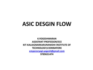
- 1. K.YOGESHWARAN ASSISTANT PROFESSOR/ECE KIT-KALAIGNARKARUNANIDHI INSTITUTE OF TECHNOLOGY,CIOMBATORE emperoryogi.yogesh@gmail.com 9789631474 ASIC DESGIN FLOW
- 2. Design Flow
- 3. LOGICAL DESIGN(FRONTEND) Consists of following steps 1.Design Entry 2.Logic Synthesis 3.System Partitioning 4.Pre Layout Simulation PHYSICAL DESIGN(BACKEND) Consists of following steps 1.Floorplanning 2.Placement 3.Routing 4.Circuit Extraction 5.Post Layout Simulation
- 4. 1. Design entry - Using a hardware description language ( HDL ) or schematic entry 2. Logic synthesis - Produces a netlist - logic cells and their connections 3. System partitioning - Divide a large system into ASIC-sized pieces 4. Prelayout simulation - Check to see if the design functions correctly 5. Floorplanning - Arrange the blocks of the netlist on the chip 6. Placement - Decide the locations of cells in a block 7. Routing - Make the connections between cells and blocks 8. Extraction - Determine the resistance and capacitance of the interconnect 9. Postlayout simulation - Check to see the design still works with the added loads of the interconnect
- 5. 1.Design Entry The designer starts the design with a text description or system specific language like HDL, C language etc. 2.Logic Synthesis Logic synthesis is the process of converting a high- level description of design into an optimized gate-level representation. It generally helps to produce the netlist consisting the description and interconnection of logic cells.
- 6. 3.System Partitioning Goal: Partition of a System into number of ASIC’s Objective: Minimize the number of external connection between each ASIC. Keep each ASIC smaller than max size.
- 7. Partitioning of a large design into a small ASIC design takes place. This is done mainly to separate different functional blocks and also to make placement and routing easier.
- 8. 4.Pre Layout Simulation Prelayout Simulation allows checking whether the design functions correct or not. Gate level functionality and timing(Delay) details can be verified. It is also called as Functional Verification.
- 9. 5.Floorplanning Goal: Calculate the size of blocks and assign them locations. Objective: Keep highly connected blocks physically close to each other. It is the first step in the physical design flow. Arrange the blocks of the netlist on the chip. It is the Tentative placement of its major functional blocks.
- 10. Slicing Floorplan: One that can be obtained by repetitively subdividing (slicing) rectangles horizontally or vertically. Non-Slicing Floorplan: One that may not be obtained by repetitively subdividing alone.
- 11. 6.Placement Goal: Assign the interconnect areas and the locations of all the logic cells with in the flexible block. Objective: Minimize the ASIC area and the interconnects. Allows the placement of cells present in the block. Assigns exact locations for various circuit components within the chip’s core area. Placement is much more suited to automation than Floorplanning.
- 13. 7.Routing Make the connections between cells and blocks. It is the process of creating physical connections based on logical connectivity. signal pins are connected by routing metal interconnects. Global Routing: Goal: Determine the location of all the interconnects. Objective: Minimize the total interconnect area. Wire segments are tentatively assigned (embedded) within the chip layout .
- 14. Detailed Routing: Goal: Completely route all the interconnects on the chip. Objective: Minimize the total interconnect length used. Find actual geometric layout of each net within assigned routing regions.
- 15. 8.Circuit Extraction Determine the resistance and capacitance of the interconnect. Basically it’s link between two domains. 1.Physical Domain 2.Electrical Domain Physical domain -it’s uses the physical information like shapes of the design. Electrical domain-provide the electrical information's (connectivity of C,R,L)
- 16. 9.Postlayout simulation Post-layout simulation you can extract the parasitic interconnect. To verify that your functional stimulus still works with accurate timing.
- 17. THANK YOU