Data flow model -Lecture-4
•Als PPTX, PDF herunterladen•
1 gefällt mir•887 views

This Data Flow Modelling - Verilog Programming is for Absolute Beginners.you can watch the video on you tube. https://youtu.be/hvfETrEGW4E

Empfohlen
Weitere ähnliche Inhalte
Was ist angesagt?
Was ist angesagt? (20)
Ähnlich wie Data flow model -Lecture-4
Ähnlich wie Data flow model -Lecture-4 (20)
Mehr von Dr.YNM
Mehr von Dr.YNM (20)
Kürzlich hochgeladen
Kürzlich hochgeladen (20)
Data flow model -Lecture-4
- 1. Digital Design Using Verilog -For Absolute Beginners LECTURE4 :DATA FLOW MODELLING
- 2. Introduction-Data Flow Modelling •For simple circuits, the gate-level modeling approach works fine because the number of gates is limited and the designer can instantiate and connect every gate individually. •Also, the gate-level modeling is very intuitive to a designer with a basic knowledge of digital logic design. •But , in complex designs where the number of gates is very large it is not the case. (that easy) •So, for efficient designing, the designers prefer a higher level of abstraction than gate level .
- 3. contd • An important point here is, as the designer is aware of how data flows between hard ware components (Registers) and how data is being processed in the design, this model is more convenient to the designers. • Another reason for importance of Data flow modelling is the unprecedented growth in the gate density on a chip which made the Gate level modelling very complicated. • Also, presently automated tools are readily available, to create a gate level circuit from data flow design description easily.(This process is called Synthesis).
- 4. contd.. • This Data Flow model is also known as Continuous Assignment model. • This type of modelling or style is more suitable for combinational logic circuits where clock is not involved as any control signal . • As the output of a logic gate is continuously driving the input of another gate ,it is popularly known as Continuous assignment model. • The Assignment statement starts with the keyword “assign” 17 June 2020 4yayavaram@yahoo.com
- 5. Continuous Assignments • A continuous assignment is the most basic statement in dataflow modeling, used to drive a value onto a net. • This assignment replaces gates in the description of the circuit and describes the circuit at a higher level of abstraction. • The assignment statement starts with the keyword assign. • For ex: assign A = B | C ( B OR C). • Similarly A = B & C • Here the assignment is continuously active. 17 June 2020 5yayavaram@yahoo.com
- 6. Contd • The assign keyword creates a static binding between RHS and LHS of the above expressions. • So, w.r.t simulation, the output is continuously active. i.e Continuous assignments are always active. • The assignment expression is evaluated as soon as one of the right-hand-side operands changes . • The operands on the right-hand side can be registers or nets or function calls. Registers or nets can be scalars or vectors. 17 June 2020 6yayavaram@yahoo.com
- 7. contd • The left hand side of an assignment must always be a scalar or vector net or a concatenation of scalar and vector nets. It cannot be a scalar or vector register. • Here net and Reg are a kind of data types. • In a simple terminology Nets represent connection between components. Ex: wire B; • Nets must be continuously driven and are used model connections between continuous assignments & instantiations. 17 June 2020 7yayavaram@yahoo.com
- 8. contd • Where as the Reg(Register) retains the last value assigned to it until another assignment statement changes their value. • Its often used to represent storage elements. • Net and Register data types can be declared as vectors (multiple bit width). • For ex: wire [3:0] a; • wire[31:0]b; • reg[7:0] c; • reg[31:0] d; 17 June 2020 8yayavaram@yahoo.com
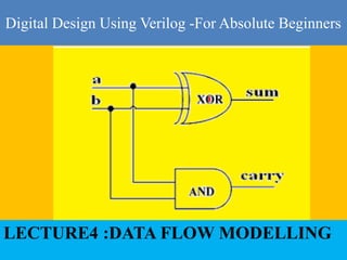
- 9. Ex 1: HALF ADDER • module Half_ adder(s,c,a,b); input a , b; // Declare input Ports output s, c; // Declare out ports assign s = a ^ b; // assign statement for x-or assign c= a & b; // assign statement for logical and endmodule. 17 June 2020 9yayavaram@yahoo.com
- 10. Ex 2: Multiplexer • The block diagram of Mux is shown below. 17 June 2020 10yayavaram@yahoo.com
- 11. contd • The out put of Mux is here S is the select line and A,B are inputs. • Here two logical ‘and’ operations, one NOT operation and one OR operations are involved. • Using the assign statements the Verilog can be written . 17 June 2020 11yayavaram@yahoo.com
- 12. Verilog code-Mux module mymux2_1(A,B,S,Y); output y; input A,B,S; assign Y= (A &(~S) | (B &S)); endmodule In the above code, & denotes logical ‘and’, ~ Denotes not , | denotes logical or operations. 17 June 2020 12yayavaram@yahoo.com
- 13. Verilog code-Mux(Aliter) The same code can also be written by another simple method shown below. module mymux2_1(A,B,S,Y); output Y; input A,B,S; assign Y= S ? B:A; endmodule Note: here ? is the conditional Operator. Y = B when S=1 else Y=A. (This is a ternary operator) 17 June 2020 13yayavaram@yahoo.com
- 14. Conditional operator (?) • ? Is a conditional operator which is a very useful ternary operator. • The conditional operator(? :) takes three operands. • Usage is ”condition-expr ? true-expr : false-expr ;” • The condition expression (condition-expr ) is first evaluated. • If the result is true (logical 1), then the true-expr is evaluated. If the result is false (logical 0), then the false-expression is evaluated. 17 June 2020 14yayavaram@yahoo.com
- 15. Ex 3: Full Adder • Full adder has three input bits and two output bits sum and carry-out as shown in the diagram below. • In the diagram A, B, Cin are inputs and Sum & Cout are outputs. 17 June 2020 15yayavaram@yahoo.com
- 16. Verilog code-Full Adder module myFA1(S,Cout,A,B,Cin); //Port declaration output S,Cout; input A,B,Cin; assign S= (A^B^Cin); //x-or operation assign Cout = (A&B | B & Cin | Cin & A); endmodule 17 June 2020 16yayavaram@yahoo.com
- 17. Full Adder -16 bit module myHA_16(S,Cout,A,B,Cin); output [15:0]S; output Cout ; input [15:0]A ; //here A,B ,S are defined as wire input [15:0] B; input Cin ; assign S[15:0] = A[15:0]^B[15:0]^Cin ; assign Cout = A[15:0]&B[15:0] | B[15:0]&Cin | Cin & A[15:0]; endmodule17 June 2020 17yayavaram@yahoo.com
- 18. 2-4 Decoder with Enable • Decoder is a combinational circuit that has ‘n’ input lines and maximum of 2n output lines. • The diagram shows a 2 to 4 Decoder with two inputs A & B , an enable pin E and four outputs D3,D2,D1,D0 . 17 June 2020 18yayavaram@yahoo.com
- 19. contd • The working of the decoder can be under stood from the truth table shown below. 17 June 2020 19yayavaram@yahoo.com
- 20. Ex: 2 to 4 Line Decoder • module decoder2_4 (A,B,E,D); input A,B,E; output [3:0]D; assign D[3] =~(~A & ~B & ~E); assign D[2] =~(~A & B & ~E); assign D[1] =~( A & ~B & ~E); assign D[0] =~( A & B & ~E); endmodule 17 June 2020 20yayavaram@yahoo.com
- 21. Ex: Half Subtractor • The diagram below shows the Half Subtractor.It has two inputs .A & B and two outputs Difference (D) and borrow(B). • Difference is given by = A ^ B • Borrow is given by Bo = 17 June 2020 21yayavaram@yahoo.com
- 22. Verilog Code • module half_sub(D,Bo,A,B); input A; input B; output D, Bo; assign D = A ^ B ; • assign borrow=(~A)&B; • endmodule 17 June 2020 22yayavaram@yahoo.com
- 23. Full Subtractor • Similar to Full adder, Full subtractor has three input bits and two output bits, Difference and Borrow. • The logic diagram is shown below. 17 June 2020 23yayavaram@yahoo.com
- 24. contd • In the diagram A,B,C are inputs ;and D and Bo are outputs. • The Difference of the Full subtractor is given by • D = A^(B^C) • Bo =(B&C)|(A&(B^C)’) 17 June 2020 24yayavaram@yahoo.com
- 25. Verilog Code • module full_sub (D,Bo,A,B,C); input A,B,C; output D, Bo; assign X = B^C; • assign D = A ^ X; • assign N =~ C; • assign Y=B & N; • assign N1 =~ X; • assign z = A & N1; • assign Bo = Y | z; • endmodule 17 June 2020 25yayavaram@yahoo.com
- 26. Verilog Code(Another way) From the Block Diagram the assignment model is • module full_sub (D,Bo,A,B,C); input A,B,C; output D, Bo; assign D = A ^ (B^C); assign Bo = B & C| (A&(B^C)’); • endmodule 17 June 2020 26yayavaram@yahoo.com
- 27. THANQ FOR WATCHING PATIENTLY 17 June 2020 27yayavaram@yahoo.com