
Empfohlen
Weitere ähnliche Inhalte
Was ist angesagt?
Was ist angesagt? (20)
Ähnlich wie Module 3 Soft lithography and LTCC.pptx
Ähnlich wie Module 3 Soft lithography and LTCC.pptx (20)
Kürzlich hochgeladen
Kürzlich hochgeladen (20)
Module 3 Soft lithography and LTCC.pptx
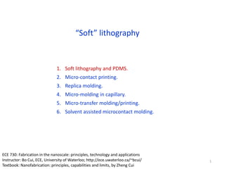
- 1. “Soft” lithography 1. Soft lithography and PDMS. 2. Micro-contact printing. 3. Replica molding. 4. Micro-molding in capillary. 5. Micro-transfer molding/printing. 6. Solvent assisted microcontact molding. 1 ECE 730: Fabrication in the nanoscale: principles, technology and applications Instructor: Bo Cui, ECE, University of Waterloo; http://ece.uwaterloo.ca/~bcui/ Textbook: Nanofabrication: principles, capabilities and limits, by Zheng Cui
- 2. Soft lithography George M. Whitesides (Harvard) Soft lithography: • Low cost • Molding, printing or transferring • Resolution usually not very high • Application in microfluidic, biomedical … “Soft” means no energetic particles (electron, ions) or radiation (UVs, X-ray) is involved. Instead, soft elastomeric stamp is used. Soft lithography opportunity assessment “Size is not the only thing that matters, function is more important” (something like this), Whiteside 2
- 3. PDMS: poly(dimethyl-siloxane) PDMS properties: • Silicone elastomer with a range of viscosities • Flexible (1 MPa Young’s modulus, typical polymer 1 GPa) and easy to mold. • Elastomer, conforms to surface over large areas. • Chemically inert, optically transparent • Low surface energy: bonds reversibly (or permanent). • Seals to flat and clean surfaces for micro-fluidic channels • Durable (reusable), low thermal expansion • Biocompatible (even used for food additive) • Environmentally safe • Best Resolution: 2-10 nm (for hard PMDS) Dow Corning brand 3
- 4. PDMS surface treatment Plasma oxidation Air (10 min) Upon treatment in oxygen plasma, PDMS seals to itself, glass, silicon, silicon nitride, and some plastic materials. contact PDMS surfaces Irreversible seal: formation of covalent bonds Biggest issue: it becomes hydrophobic quickly, very bad for micro-fluidic applications. (liquid hard to get into the channels once it becomes hydrophobic) PMDS is absolutely the most popular material for bio-medical lab-on-chip (microfluidic) applications, but may not be suitable for commercial applications, which need chemically stable surface. 4
- 5. PDMS problems: soft, low Young’s modulus Shrinking makes accurate (< few m) alignment very difficult. 5
- 6. “Soft” lithography 1. Soft lithography and PDMS. 2. Micro-contact printing. 3. Replica molding. 4. Micro-molding in capillary. 5. Micro-transfer molding/printing. 6. Solvent assisted microcontact molding. 6
- 7. Micro - contact printing (μCP) 100mm stamp 20m 7
- 8. Test structures in Au, smallest dimension 400nm Micro - contact printing (μCP) 8
- 9. Micro - contact printing (μCP), with roller Xia & Whitesides, Angew. Chem. Int. Ed. 1998, 37, 550-575. A. Kumar & G. Whitesides, Applied Physics Lett. 1993 a. Printing on a planar surface with a planar stamp. b. Printing on a planar surface with a rolling stamp c. Printing on a non-planar surface with a planar stamp 9
- 10. Substrate Molecules Popular “ink” molecules 10
- 11. “Soft” lithography 1. Soft lithography and PDMS. 2. Micro-contact printing. 3. Replica molding. 4. Micro-molding in capillary. 5. Micro-transfer molding/printing. 6. Solvent assisted microcontact molding. 11
- 12. Replica molding (REM) Xia & Whitesides et al, Advanced Materials, 1997, 9, 147 PU = polyurethane It is similar to UV-curing nanoimprint lithography 12
- 13. Replica molding (REM) The patterning process has high fidelity, with little feature size loss. 13
- 15. “Soft” lithography 1. Soft lithography and PDMS. 2. Micro-contact printing. 3. Replica molding. 4. Micro-molding in capillary. 5. Micro-transfer molding/printing. 6. Solvent assisted microcontact molding. 15
- 16. Uses capillary forces to fill the gaps between substrate and PDMS master. 1. The PDMS master is pressed tightly on a planar substrate. 2. Elastic PDMS seals off walls and creates capillary channels. 3. A drop of liquid prepolymer is placed at the ends of these channels and fills them automatically due to capillary force. 4. PDMS can absorb the solvent, which creates a partial vacuum inside the PDMS cavity and helps to draw in liquid polymer. 5. Cure and peel of the PDMS master. Micro-molding in capillary (MIMIC) Line-width: 100nm Liquid pre- polymer Nano-molding in capillaries is possible 16
- 17. Micro-molding in capillary (MIMIC) Kim & Whitesides et al, Nature, 1995, 376, 581 Xia, Y.; Whitesides, G. M. Ann. Rev. Mater. Sci 1998, 28, 153. a: PU (polyurethane) on Si b: polyaniline c: ZrO2 d: polystryene colloids e+f: free standing PU 17
- 18. “Soft” lithography 1. Soft lithography and PDMS. 2. Micro-contact printing. 3. Replica molding. 4. Micro-molding in capillary. 5. Micro-transfer molding/printing. 6. Solvent assisted microcontact molding. 18
- 19. • Apply the liquid prepolymer • Planarize the prepolymer • Place the master on a planar substrate • UV exposure or heating solidifies the prepolymer that sticks to the substrate Micro - transfer molding (μTM) TM fabrication of a). one-layer microstructures; b). three-layer polymer microstructures. PDMS Pre-polymer Substrate 19
- 20. Micro - transfer molding (μTM) Zhao & Whitesides et al, Advanced Materials, 1996, 8, 837. Microstructures fabricated using TM. a) An SEM image of a fractured sample showing a pattern of isolated stars of UV-cured polyurethane (NOA 73) on Ag. b) An array of parallel lines of spin-on glass on Si with an aspect ratio (height/width) of 8. c) A two-layer structure: isolated micro-cylinders (1.5m in diameter) on 5m-wide lines, supported on a glass cover slide. d) A two-layer structure: a continuous web over a layer of 5m-wide lines, supported on a glass cover slide. e) A three-layer structure on a glass cover slide. The layers of 4 m-wide lines are oriented at 60o from each other. Structures in c-e were made of heat-cured epoxy (F109CLR). 20
- 21. Metal transfer assisted nanolithography a) SEM image of the transferred metal grating onto PMMA layer with period of 700nm on SiO2 substrate. b) Period 220nm on PET substrate. c) After O2 RIE of b. d) After metallization and lift-off process of c. Guo, “Metal transfer assisted nanolithography on rigid and flexible substrates”, JVST B, 2008 21 Glass transition temperature is 105oC
- 22. Metal transfer assisted nanolithography: line-width reduction Schematic of shadow (angle) evaporation of metals to reduce pattern line-width. The line-width is reduced by the thickness of the metal on the PDMS grating sidewall. SEM image of the metal grating on PET substrate after line-width reduction. The inset is a zoom-in view showing that the line-width was reduced to 50nm. 22
- 23. “Soft” lithography 1. Soft lithography and PDMS. 2. Micro-contact printing. 3. Replica molding. 4. Micro-molding in capillary. 5. Micro-transfer molding/printing. 6. Solvent assisted microcontact molding. 23
- 24. Solvent assisted microcontact molding (SAMIM) (solvent assisted imprinting) Kim & Whitesides et al, Advanced Materials, 1997, 9,651. Substrates Silicon Glass Flexible transparency Polymer SU-8 (1μm) Shipley 1805 Photoresist (500nm) 3% PMMA (70nm) Solvent SU-8 (ethanol) Shipley 1805 photoresist (ethanol) 3% PMMA (acetone) Uses a solvent to wet the PDMS stamp and soften the structure polymer. Dissipate and evaporate the solvent through PDMS. (PDMS stamp can absorb the solvent because of the solvent permeability of PDMS.) The molded polymer structure becomes solidified in a few minutes after evaporation of solvent, while the stamp is still in conformable contact with the substrate. 24
- 25. SAMIM of SU-8 in ethanol SU-8 2m diameter 25
- 26. SAMIM of PMMA in acetone Au structure fabrication 26
- 27. Advantages: • Convenient and low cost • Rapid prototyping • Deformation of PDMS provides route to complex patterns • No optical diffraction limit • Non-planar or curved surfaces • Generation of 3D -structures • Control over surface chemistry • A broad range of materials • Applicable to manufacturing • Patterning over large areas Disadvantages: • Distortion of patterns • Poor registration/alignment • Compatibility with IC processes • Defects and their densities • μCP can only be applied to a number of surfaces • MIMIC is a relatively slow process Soft lithography: advantages and disadvantages 27
- 28. PDMS elastomer for mold making 28
- 29. PDMS elastomer for mold making 29
- 30. PDMS elastomer for mold making 30
- 31. PDMS elastomer for mold making 31
- 32. PDMS elastomer for mold making University of Washington (coat mold release agent) 32
- 33. 33
- 34. Low temperature co-fired ceramic processing • The very rapid evolution of semiconductor IC technology has put immense pressure on the packaging technologies. • The new packages must have increasingly smaller footprints, simultaneously offering improved performance in handling high frequency clocks, very large number of pin-outs and capability to handle and dissipate large heat densities. • In other realms there is a need for multilayer solution for miniaturizing the HF circuits in GHz range, while the Micro Electro Mechanical System (MEMS) devices need an one technology solution for packaging sensors / actuators requiring electrical, optical, fluidic and mechanical ‘interconnects’. • The Low Temperature Co-fired Ceramic (LTCC) Technology offers and ‘integrated’ solutions to these problems.
- 35. LTCC (Low Temperature Co-fired Ceramics) is a multi-layer glass ceramic substrate which is Co-fired with low resistance metal conductors at low firing temperature (less than 1000℃). It is sometimes referred to as "Glass Ceramics" because its composition consists of glass and alumina.
- 36. Low temperature co-fired ceramic processing
- 37. Low temperature co-fired ceramic processing
- 38. LTCC Fabrication Process • The process starts with via punching of each layer as per individual layer design. • If the layer requires any open or buried cavity, it is prepared using the same machine. • The alignment holes are also punched using via puncher. • Via filling is done subsequently, using stencil printing. • This is followed by screen printing of conductor pattern using usual screen printing process. • Once individual layers are ready, those layers are stacked in sequence, and aligned mechanically. • The stacks are then sealed in a plastic bag are and laminated under prescribed temperature- pressure cycle using isostatic laminator. • The individual circuits are then singulated using cutter and fired using a special programmable batch furnace. • All the fabrication processes described above, are carried out in Class 10000 Clean Room. • For preparing packages, there are two main post firing processes that remain at this stage. One, processes for preparing BGA, and second, processes for sealing. We have chosen two possible options for sealing processes, viz. Solder sealing and Seam sealing and three BGA formation processes, viz. sphere attachment, stencil printing and electroplating. Following is the brief description of sealing and BGA formation processes.
- 39. Solder sealing Solder sealing is done using solder performs. This needs conducting and solderable surfaces on either side. Further, interconnection from lid to base would also require similar pads. As per present plan, these conducting surfaces would be made using a co-fired Ag-Pd paste. Finally, solder sealing is done by reflow after components are placed. Seam Sealing Seam sealing requires brazing of metallic parts to the ceramic substrate. Brazing is a three step process that requires post-fire adhesion layer, post fire barrier layer, brazing layer, each being individually printed and fired. The brazing layer is a low temperature alloy, and is required to be fired with the metallic part. The BGA could then be formed by one of the processes described below. It may be noted here that final sealing process by seam sealing can be done only after components are placed inside the base. BGA Formation Processes The three process options selected here have their own advantages and disadvantages. Sphere attachment is done using pre-formed solder spheres which could be attached using another solder paste or through reflow of the same BGA spheres. This process is simple, and cheap, but has limitations in terms of minimum BGA size. The stencil printing process is also cheap, slightly more process dependent but can make BGAs with sizes up to even 100µm but with relaxed pitch. The electroplating process is having more process steps making it costlier, but is capable of even sub-100µm BGA with equal pitch. Through the present project we are attempting an exploration of each one of this process. The materials selection for each process has to be done very carefully so as to ensure subsequently lower temperature steps.
- 40. Sphere Attachment BGA by solder sphere attachment is done by directly placing micro-spheres of high-Pb solder on conducting pads with high alignment accuracy. The solder pads are dispensed with a viscous flux or attachment solder paste prior to this placement. Reflow of these solder spheres or attachment solder paste would produce BGAs. Stencil printing For good adhesion, one requires Under Bump Metallurgy (UBM) or adhesion / barrier layers before solder deposition. High lead Sn-Pb Solder is deposited by printing solder paste onto the Under Bump Metallurgy (UBM) by stencil printing process and reflowing the solder paste to form a spherical solder bump. Electroplating In this case the UBM consists typically of an evaporated adhesion layer that provides conducting path for electroplating, followed by photolithography to open areas of BGA pads. The BGA pads are then electroplated with adhesion enhancing and solder-barrier layers. Plating of the high lead Sn-Pb solder alloy is then done over the UBM followed by removal of resist and underlying evaporated seed layer. The final step is of reflow that forms the solder bump.
- 41. LTCC Advantages •Multilayer capability- means interconnect density limited only by the installed process capabilities •Compatibility with flip chip process means capability to handle and redistribute large number of I/Os •Capability to integrate passives means appropriation of additional components within the package which otherwise are accommodated out of the package •HF capability up to millimeter wave… means integration of front-end modules in communication devices •Integration of Si and other technology devices simultaneously Flexibility to choose integration scheme •but the system designer has to work in tandem with chip manufacturers Ceramic process brings high reliability •Capability of handling electrical, optical, fluidic and mechanical interconnects in and out of the package Amenable to automated wafer assembly; useful tool for fast prototyping •TCE matching with semiconductor device materials High working temperature
- 42. Application examples - Nozzles that require conductors. • Nozzle for atmospheric pressure plasma cleaning equipment. It is possible to appropriately design the internal conductor pattern shape and the distance between conductors depending on the type of gas used. The shape for rectification at the nozzle tip is also available. - Substrate utilizing the hollow as a flow path. • Sensor unit that analyzes gas and liquid components. • Substrate that resists high temperatures by the flow of cooling gas and liquid through it. - Substrate with special characteristics, created by filling the hollow part with a different material. • Substrate with excellent high frequency characteristics. • Substrate filled with high shielding material to reduce signal interference. • High heat dissipation substrate filled with high heat dissipation material. - Built-in integrated component substrate for miniaturization and space saving. (Note: The mounting part requires an opening) • Component mounting, or built-in cavity substrate. - Substrate that requires partial thermal insulation due to product configuration. • Substrate where the effective temperature range differs between the upper and lower