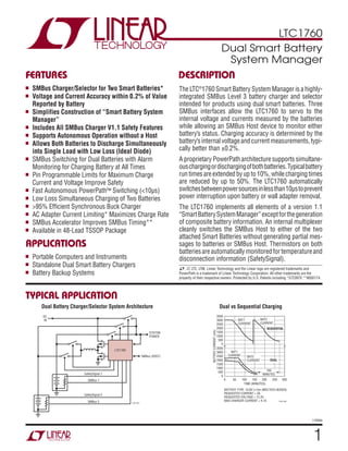
SlideShare ist ein Scribd-Unternehmen logo
1 von 48
Downloaden Sie, um offline zu lesen
LTC1760
1
1760fa
TYPICAL APPLICATION
FEATURES DESCRIPTION
Dual Smart Battery
System Manager
The LTC®
1760 Smart Battery System Manager is a highly-
integrated SMBus Level 3 battery charger and selector
intended for products using dual smart batteries. Three
SMBus interfaces allow the LTC1760 to servo to the
internal voltage and currents measured by the batteries
while allowing an SMBus Host device to monitor either
battery’s status. Charging accuracy is determined by the
battery’sinternalvoltageandcurrentmeasurements,typi-
cally better than ±0.2%.
A proprietary PowerPatharchitecture supports simultane-
ouschargingordischargingofbothbatteries.Typicalbattery
run times are extended by up to 10%, while charging times
are reduced by up to 50%. The LTC1760 automatically
switchesbetweenpowersourcesinlessthan10μstoprevent
power interruption upon battery or wall adapter removal.
The LTC1760 implements all elements of a version 1.1
“SmartBatterySystemManager”exceptforthegeneration
of composite battery information. An internal multiplexer
cleanly switches the SMBus Host to either of the two
attached Smart Batteries without generating partial mes-
sages to batteries or SMBus Host. Thermistors on both
batteriesareautomaticallymonitoredfortemperatureand
disconnection information (SafetySignal).
Dual vs Sequential Charging
APPLICATIONS
n SMBus Charger/Selector for Two Smart Batteries*
n Voltage and Current Accuracy within 0.2% of Value
Reported by Battery
n Simplifies Construction of “Smart Battery System
Manager”
n Includes All SMBus Charger V1.1 Safety Features
n Supports Autonomous Operation without a Host
n Allows Both Batteries to Discharge Simultaneously
into Single Load with Low Loss (Ideal Diode)
n SMBus Switching for Dual Batteries with Alarm
Monitoring for Charging Battery at All Times
n Pin Programmable Limits for Maximum Charge
Current and Voltage Improve Safety
n Fast Autonomous PowerPath™ Switching (<10μs)
n Low Loss Simultaneous Charging of Two Batteries
n >95% Efficient Synchronous Buck Charger
n AC Adapter Current Limiting* Maximizes Charge Rate
n SMBus Accelerator Improves SMBus Timing**
n Available in 48-Lead TSSOP Package
n Portable Computers and Instruments
n Standalone Dual Smart Battery Chargers
n Battery Backup Systems
LTC1760
DC
IN
SYSTEM
POWER
SMBus (HOST)
1760 TA01
SafetySignal 1
SMBus 1
SafetySignal 2
SMBus 2
TIME (MINUTES)
BATTERYCURRENT(mA)
3500
3000
2500
2000
1500
1000
500
0
3500
3000
2500
2000
1500
1000
500
0
1760 TA03
0 50 100 150 200 250 300
BAT1
CURRENT
BAT2
CURRENT
SEQUENTIAL
DUAL
BAT1
CURRENT
100
MINUTES
BATTERY TYPE: 10.8V Li-Ion (MOLTECH NI2020)
REQUESTED CURRENT = 3A
REQUESTED VOLTAGE = 12.3V
MAX CHARGER CURRENT = 4.1A
BAT2
CURRENT
Dual Battery Charger/Selector System Architecture
L, LT, LTC, LTM, Linear Technology and the Linear logo are registered trademarks and
PowerPath is a trademark of Linear Technology Corporation. All other trademarks are the
property of their respective owners. Protected by U.S. Patents including *5723970 **6650174.
LTC1760
2
1760fa
PIN CONFIGURATIONABSOLUTE MAXIMUM RATINGS
DCIN, SCP, SCN, CLP,
VPLUS, SW to GND.....................................–0.3V to 32V
SCH1, SCH2 to GND...................................–0.3V to 28V
BOOST to GND...........................................–0.3V to 37V
CSP, CSN, BAT1, BAT2 to GND...................–0.3V to 28V
LOPWR, DCDIV to GND ............................. –0.3V to 10V
VCC2, VDDS to GND.......................................–0.3V to 7V
SDA1, SDA2, SDA, SCL1,
SCL2, SCL, SMBALERT to GND....................–0.3V to 7V
MODE to GND .................................–0.3V to VCC2 +0.3V
COMP1 to GND............................................–0.3V to 5V
Maximum DC Current Into Pin
SDA1, SDA2, SDA, SCL1, SCL2, SCL ................ ±3mA
TH1A, TH2A..................................................... –5mA
TH1B, TH2B ................................................... –102μA
Operating Junction Temperature Range
(Note 6).................................................. –40°C to 125°C
Storage Temperature..............................–65°C to 150°C
Lead Temperature (Soldering, 10 sec)...................300°C
(Note 1)
1
2
3
4
5
6
7
8
9
10
11
12
13
14
15
16
17
18
19
20
21
22
23
24
TOP VIEW
FW PACKAGE
48-LEAD PLASTIC TSSOP
48
47
46
45
44
43
42
41
40
39
38
37
36
35
34
33
32
31
30
29
28
27
26
25
SCH2
GCH2
GCH1
SCH1
TGATE
BOOST
SW
DCIN
VCC
BGATE
PGND
COMP1
CLP
CSP
CSN
VLIMIT
ILIMIT
TH1B
TH1A
SMBALERT
TH2A
TH2B
MODE
VCC2
VPLUS
BAT2
BAT1
SCN
SCP
GDCO
GDCI
GB1O
GB1I
GB2O
GB2I
LOPWR
VSET
ITH
ISET
DCDIV
SCL2
SCL
SCL1
VDDS
SDA2
SDA
SDA1
GND
TJMAX = 125°C, θJA = 110°C/W
ORDER INFORMATION
LEAD FREE FINISH TAPE AND REEL PART MARKING PACKAGE DESCRIPTION TEMPERATURE RANGE
LTC1760CFW#PBF LTC1760CFW#TRPBF LTC1760CFW 48-Lead Plastic TSSOP 0°C to 85°C
LTC1760IFW#PBF LTC1760IFW#TRPBF LTC1760IFW 48-Lead Plastic TSSOP –40°C to 125°C
Consult LTC Marketing for parts specified with wider operating temperature ranges.
Consult LTC Marketing for information on non-standard lead based finish parts.
For more information on lead free part marking, go to: http://www.linear.com/leadfree/
For more information on tape and reel specifications, go to: http://www.linear.com/tapeandreel/
LTC1760
3
1760fa
ELECTRICAL CHARACTERISTICS
SYMBOL PARAMETER CONDITIONS MIN TYP MAX UNITS
Supply and Reference
DCIN Operating Range DCIN Selected 6 28 V
ICH0
ICH1
DCIN Operating Current Not Charging (DCIN Selected) (Note 10)
Charging (DCIN Selected) (Note 10)
1
1.3
1.5
2
mA
mA
IVCC2_AC1
IVCC2_AC0
VCC2 Operating Current AC Present (Note 11)
AC Not Present (Note 11)
0.75
75
1
100
mA
μA
Battery Operating Voltage Range Battery Selected, PowerPath Function
Battery Selected, Charging Function (Note 2)
6
0
28
28
V
V
IBAT Battery Drain Current Battery Selected, Not Charging, VDCIN = 0V (Note 10) 175 μA
VFDC
VFB1
VFB2
VFSCN
VPLUS Diodes Forward Voltage:
DCIN to VPLUS
BAT1 to VPLUS
BAT2 to VPLUS
SCN to VPLUS
IVCC = 10mA
IVCC = 0mA
IVCC = 0mA
IVCC = 0mA
0.8
0.7
0.7
0.7
V
V
V
V
UVLO Undervoltage Lockout Threshold VPLUS Ramping Down, Measured at VPLUS to GND l 3 5 V
VVCC VCC Regulator Output Voltage l 4.9 5.2 5.5 V
VLDR VCC Load Regulation IVCC = 0mA to 10mA l 0.2 1 %
Switching Regulator
VTOL Voltage Accuracy With Respect to Voltage Reported by Battery
VCHMIN < Requested Voltage < VLIMIT
l –32 32 mV
ITOL Current Accuracy With Respect to Current Reported by Battery
4mV/RSENSE < Requested Current < ILIMIT (Min)
(Note 12)
RILIMIT = 0 (Short to GND)
RILIMIT = 10k ±1%
RILIMIT = 33k ±1%
RILIMIT = Open (or Short ILIMIT to VCC2)
l
l
l
l
–2
–4
–8
–8
2
4
8
8
mA
mA
mA
mA
f0SC Regulator Switching Frequency 255 300 345 kHz
fDO Regulator Switching Frequency in Low
Dropout Mode
Duty Cycle ≥99% 20 25 kHz
DCMAX Regulator Maximum Duty Cycle 99 99.5 %
IMAX Maximum Current Sense Threshold VITH = 2.2V 140 155 190 mV
ISNS CA1 Input Bias Current VCSP = VCSN > 5V 150 μA
CMSL CA1 Input Common Mode Low 0 V
CMSH CA1 Input Common Mode High VDCIN – 0.2 V
VCL1 CL1 Turn-On Threshold
C-Grade (Note 6)
I-Grade (Note 6)
l
l
95
94
90
100
100
100
105
108
108
mV
mV
mV
TG tr
TG tr
TGATE Transition Time:
TGATE Rise Time
TGATE Fall Time
CLOAD = 3300pF, 10% to 90%
50
50
90
90
ns
ns
BG tr
BG tf
BGATE Transition Time
BGATE Rise Time
BGATE Fall Time
CLOAD = 3300pF, 10% to 90%
50
40
90
80
ns
ns
The l denotes the specifications which apply over the full operating
junction temperature range, otherwise specifications are at TA = 25°C (Note 6). VDCIN = 20V, VBAT1 = 12V, VBAT2 = 12V, VVDDS = 3.3V,
VVCC2 = 5.2V unless otherwise noted.
LTC1760
4
1760fa
SYMBOL PARAMETER CONDITIONS MIN TYP MAX UNITS
Trip Points
VTR DCDIV/LOPWR Threshold VDCDIV or VLOPWR Falling
C-Grade (Note 6)
I-Grade (Note 6)
l
l
1.166
1.162
1.19
1.19
1.215
1.215
V
V
VTHYS DCDIV/LOPWR Hysteresis Voltage VDCDIV or VLOPWR Rising 30 mV
IBVT DCDIV/LOPWR Input Bias Current VDCDIV or VLOPWR = 1.19V 20 200 nA
VTSC Short-Circuit Comparator Threshold VSCP – VSCN, VCC ≥ 5V
C-Grade (Note 6)
I-Grade (Note 6)
l
l
90
88
100
100
115
115
mV
mV
VFTO Fast PowerPath Turn-Off Threshold VDCDIV Rising from VCC 6 7 7.9 V
VOVSD Overvoltage Shutdown Threshold as a
Percent of Programmed Charger Voltage
VSET Rising from 0.8V until TGATE and BGATE
Stop Switching
107 %
DACs
IRES IDAC Resolution Guaranteed Monotonic 10 Bits
tIP
tILOW
IDAC Pulse Period:
Normal Mode
Wake-Up Mode
6 10
50
15 μs
ms
Charging Current Granularity RILIMIT = 0 (Short ILIMIT to GND)
RILIMIT = 10k ±1%
RILIMIT = 33k ±1%
RILIMIT = Open (or Short ILIMIT to VCC2 )
1
2
4
4
mA
mA
mA
mA
IWAKE_UP Wake-Up Charging Current (Note 5) 60 80 100 mA
ILIMIT Charging Current Limit C-Grade (Note 6)
RILIMIT = 0 (Short ILIMIT to GND)
RILIMIT = 10k ±1%
RILIMIT = 33k ±1%
RILIMIT = Open (or Short ILIMIT to VCC2 )
I-Grade (Note 6)
RILIMIT = 0 (Short ILIMIT to GND)
RILIMIT = 10k ±1%
RILIMIT = 33k ±1%
RILIMIT = Open (or Short ILIMIT to VCC2 )
l
l
l
l
l
l
l
l
980
1960
2490
3920
930
1870
2380
3750
1000
2000
3000
4000
1000
2000
3000
4000
1070
2140
3210
4280
1110
2220
3320
4430
mA
mA
mA
mA
mA
mA
mA
mA
VRES VDAC Resolution Guaranteed Monotonic (5V < VBAT < 25V) 11 Bits
VSTEP VDAC Granularity 16 mV
VLIMIT Charging Voltage Limit
(Note 7)
RVLIMIT = 0 (Short VLIMIT to GND)
RVLIMIT = 10k ±1%
RVLIMIT = 33k ±1%
RVLIMIT = 100k ±1%
RVLIMIT = Open (or Short VLIMIT to VCC2 )(Note 13)
l
l
l
l
l
8400
12608
16832
21024
8432
12640
16864
21056
32768
8464
12672
16896
21088
mV
mV
mV
mV
mV
Charge MUX Switches
tONC GCH1/GCH2 Turn-On Time VGCHX – VSCHX > 3V, CLOAD = 3000pF 5 10 ms
tOFFC GCH1/GCH2 Turn-Off Time VGCHX – VSCHX < 1V, from Time of
VCSN < VBATX – 30mV, CLOAD = 3000pF
15 μs
VCON CH Gate Clamp Voltage
GCH1
GCH2
ILOAD = 1μA
VGCH1 – VSCH1
VGCH2 – VSCH2
5
5
5.8
5.8
7
7
V
V
ELECTRICAL CHARACTERISTICS The l denotes the specifications which apply over the full operating
junction temperature range, otherwise specifications are at TA = 25°C (Note 6). VDCIN = 20V, VBAT1 = 12V, VBAT2 = 12V, VVDDS = 3.3V,
VVCC2 = 5.2V unless otherwise noted.
LTC1760
5
1760fa
SYMBOL PARAMETER CONDITIONS MIN TYP MAX UNITS
VCOFF CH Gate Off Voltage
GCH1
GCH2
ILOAD =10μA
VGCH1 – VSCH1
VGCH2 – VSCH2
–0.8
–0.8
–0.4
–0.4
0
0
V
V
VTOC CH Switch Reverse Turn-Off Voltage VBATX – VCSN, 5V ≤ VBATX ≤ 28V
C-Grade (Note 6)
I-Grade (Note 6)
l
l
5
2
20
20
40
40
mV
mV
VFC CH Switch Forward Regulation Voltage VCSN – VBATX, 5V ≤ VBATX ≤ 28V l 15 35 60 mV
IOC(SRC)
IOC(SNK)
GCH1/GCH2 Active Regulation:
Max Source Current
Max Sink Current
VGCHX – VSCHX = 1.5V
–2
2
μA
μA
VCHMIN BATX Voltage Below Which
Charging is Inhibited
(Note 14) 3.5 4.7 V
PowerPath Switches
tDLY Blanking Period after UVLO Trip Switches Held Off 250 ms
tPPB Blanking Period after LOPWR Trip Switches in 3-Diode Mode 1 sec
tONPO GB1O/GB2O/GDCO Turn-On Time VGS < –3V, from Time of Battery/DC
Removal, or LOPWR Indication, CLOAD = 3000pF
l 5 10 μs
tOFFPO GB1O/GB2O/GDCO Turn-Off Time VGS > –1V, from Time of Battery/DC
Removal, or LOPWR Indication, CLOAD = 3000pF
l 3 7 μs
VPONO Output Gate Clamp Voltage
GB1O
GB2O
GDCO
ILOAD = 1μA
Highest (VBAT1 or VSCP) – VGB1O
Highest (VBAT2 or VSCP) – VGB2O
Highest (VDCIN or VSCP) – VGDCO
4.75
4.75
4.75
6.25
6.25
6.25
7
7
7
V
V
V
VPOFFO Output Gate Off Voltage
GB1O
GB2O
GDCO
ILOAD = –25μA
Highest (VBAT1 or VSCP) – VGB1O
Highest (VBAT2 or VSCP) – VGB2O
Highest (VDCIN or VSCP) – VGDCO
0.18
0.18
0.18
0.25
0.25
0.25
V
V
V
VTOP PowerPath Switch Reverse
Turn-Off Voltage
VSCP – VBATX or VSCP – VDCIN
6V ≤ VSCP ≤ 28V
C-Grade (Note 6)
I-Grade (Note 6)
l
l
5
2
20
20
60
60
mV
mV
VFP PowerPath Switch Forward
Regulation Voltage
VBATX – VSCP or VDCIN – VSCP
6V ≤ VSCP ≤ 28V
l 0 25 50 mV
IOP(SRC)
IOP(SNK)
GDCI/GB1I/GB2I Active Regulation:
Source Current
Sink Current
(Note 3)
–4
75
μA
μA
tONPI Gate B1I/B2I/DCI Turn-On Time VGS < –3V, CLOAD = 3000pF (Note 4) 300 μs
tOFFPI Gate B1I/B2I/DCI Turn-Off Time VGS > –1V, CLOAD = 3000pF (Note 4) 10 μs
VPONI Input Gate Clamp Voltage
GB1I
GB2I
GDCI
ILOAD = 1μA
Highest (VBAT1 or VSCP) – VGB1I
Highest (VBAT2 or VSCP) – VGB2I
Highest (VDCIN or VSCP) – VGDCI
4.75
4.75
4.75
6.7
6.7
6.7
7.5
7.5
7.5
V
V
V
VPOFFI Input Gate Off Voltage
GB1I
GB2I
GDCI
ILOAD = –25μA
Highest (VBAT1 or VSCP) – VGB1I
Highest (VBAT2 or VSCP) – VGB2I
Highest (VDCIN or VSCP) – VGDCI
0.18
0.18
0.18
0.25
0.25
0.25
V
V
V
ELECTRICAL CHARACTERISTICS The l denotes the specifications which apply over the full operating
junction temperature range, otherwise specifications are at TA = 25°C (Note 6). VDCIN = 20V, VBAT1 = 12V, VBAT2 = 12V, VVDDS = 3.3V,
VVCC2 = 5.2V unless otherwise noted.
LTC1760
6
1760fa
SYMBOL PARAMETER CONDITIONS MIN TYP MAX UNITS
Thermistor
Thermistor Trip
COLD-RANGE to OVER-RANGE
CLOAD(MAX) = 300pF (Note 9)
R1A = R2A = 1130Ω ±1%
R1B = R2B = 54900Ω ±1%
l 95 100 105 kΩ
Thermistor Trip
IDEAL-RANGE to COLD-RANGE
CLOAD(MAX) = 300pF (Note 9)
R1A = R2A = 1130Ω ±1%
R1B = R2B = 54900Ω ±1%
l 28.5 30 32.5 kΩ
Thermistor Trip
HOT-RANGE to IDEAL-RANGE
CLOAD(MAX) = 300pF (Note 9)
R1A = R2A = 1130Ω ±1%
R1B = R2B = 54900Ω ±1%
C-Grade (Note 6)
I-Grade (Note 6)
l
l
2.85
2.83
3
3
3.15
3.15
kΩ
kΩ
Thermistor Trip
UNDER-RANGE to HOT-RANGE
CLOAD(MAX) = 300pF (Note 9)
R1A = R2A = 1130Ω ±1%
R1B = R2B = 54900Ω ±1%
l 425 500 575 Ω
Logic Levels
SCL/SCL1/SCL2/SDA/SDA1/
SDA2 Input Low Voltage (VIL)
l 0.8 v
SCL/SCL1/SCL2/SDA/SDA1/
SDA2 Input High Voltage (VIH)
l 2.1 v
SCL/SCL1/SCL2/SDA/SDA1/
SDA2 Input Leakage Current
VSDA, VSCL, VSDA1, VSCL1,
VSDA2, VSCL2 = 0.8V
l –5 5 μA
SCL/SCL1/SCL2/SDA/SDA1/
SDA2 Input Leakage Current
VSDA, VSCL, VSDA1, VSCL1, VSDA2,
VSCL2 = 2.1V
l –5 5 μA
IPULLUP SCL1/SDA1/SCL2/SDA2 Pull-Up
Current When Not Connected to
SMBus Host
VSCL1, VSDA1, VSCL2, VSDA2 = 0.4V
VVCC2 = 4.85V and 5.55V (Current is Through
Internal Series Resistor and Schottky to VCC2)
165 220 350 μA
SCL1/SDA1/SCL2/SDA2
Series Impedance to Host SMBus
VSDA1, VSCL1, VSDA2, VSCL2 = 0.8V l 300 Ω
SCL/SDA Output Low Voltage (VOL).
LTC1760 Driving the Pin
IPULLUP = 350μA l 0.4 V
SCL1/SDA1/SCL2/SDA2 Pullup
Output Low Voltage (VOL).
LTC1760 Driving the Pin with Battery
SMBus not Connected to Host SMBus
IPULLUP Internal to LTC1760 l 0.4 V
SCL1/SDA1/SCL2/SDA2
Output Low Voltage (VOL).
LTC1760 Driving the Pin with Battery
SMBus Connected to Host SMBus
IPULLUP = 350μA on Host Side l 0.4 V
SCL/SCL1/SCL2/SDA/SDA1/ SDA2/
SMBALERT Power Down Leakage
VVCC2 = 0V, VVDDS = 0V,
VSCL, VSCL1, VSCL2, VSDA,
VSDA1, VSDA2, VSMBALERT = 5.5V
l 2 μA
SMBALERT Output Low Voltage (VOL) IPULLUP = 500μA l 0.4 V
SMBALERT Output Pull-Up Current VSMBALERT = 0.4V 3.5 10 17.5 μA
VIL_VDDS
VIH_VDDS
VDDS Input Low Voltage (VIL)
VDDS Input High Voltage (VIH)
VDDS Operating Voltage
VDDS Operating Current VSCL, VSDA = VVDDS , VVDDS = 5V
l
l
l
2.6
3
1.5
5.5
18
V
V
V
μA
VIL_MODE MODE Input Low Voltage (VIL) VVCC2 = 4.85V l VVCC2 • 0.3 V
ELECTRICAL CHARACTERISTICS The l denotes the specifications which apply over the full operating
junction temperature range, otherwise specifications are at TA = 25°C (Note 6). VDCIN = 20V, VBAT1 = 12V, VBAT2 = 12V, VVDDS = 3.3V,
VVCC2 = 5.2V unless otherwise noted.
LTC1760
7
1760fa
SYMBOL PARAMETER CONDITIONS MIN TYP MAX UNITS
VIH_MODE MODE Input High Voltage (VIH) VVCC2 = 4.85V l VVCC2 • 0.7 V
MODE Input Current (IIH) MODE = VVCC2 • 0.7V, VVCC2 = 4.85V l –1 1 μA
MODE Input Current (IIL) MODE = VVCC2 • 0.3V, VVCC2 = 4.85V l –1 1 μA
Charger Timing
tTIMEOUT Timeout for Wake-Up Charging and
Controlled Charging
l 140 175 210 sec
tQUERY Sampling Rate Used by the LTC1760 to
Update Charging Parameters
1 sec
SMBus Timing
SCL Serial-Clock High Period(tHIGH) At IPULLUP = 350μA, CLOAD = 150pF (Note 8) l 4 μs
SCL Serial-Clock Low Period (tLOW) At IPULLUP = 350μA, CLOAD = 150pF (Note 8) l 4.7 μs
SDA/SCL Rise Time (tr) CLOAD = 150pF, RPU = 9.31k (Note 8) l 1000 ns
SDA/SCL Fall Time (tf) CLOAD = 150pF, RPU = 9.31k (Note 8) l 300 ns
SMBus Accelerator Trip Voltage Range l 0.8 1.42 V
Start-Condition Setup Time (tSU:STA) l 4.7 μs
Start-Condition Hold Time (tHD:STA) l 4 μs
SDA to SCL Rising-Edge
Setup Time (tSU:DAT)
l 250 ns
SDA to SCL Falling-Edge Hold Time,
Slave Clocking in Data (tHD:DAT)
l 300 ns
tTIMEOUT_
SMB
The LTC1760 will Release the SMBus
and Terminate the Current Master or
Slave Command if the Command is not
Completed Before this Time
l 25 35 ms
ELECTRICAL CHARACTERISTICS The l denotes the specifications which apply over the full operating
junction temperature range, otherwise specifications are at TA = 25°C (Note 6). VDCIN = 20V, VBAT1 = 12V, VBAT2 = 12V, VVDDS = 3.3V,
VVCC2 = 5.2V unless otherwise noted.
Note 1: Stresses beyond those listed under Absolute Maximum Ratings
may cause permanent damage to the device. Exposure to any Absolute
Maximum Rating condition for extended periods may affect device
reliability and lifetime.
Note 2: Battery voltage must be adequate to drive gates of PowerPath
P-channel FET switches. This does not affect charging voltage of the
battery, which can be zero volts during wake-up charging.
Note 3: DCIN, BAT1, BAT2 are held at 12V and GDCI, GB1I, GB2I are
forced to 10.5V. SCP is set at 12V to measure source current at GDCI,
GB1I and GB2I. SCP is set at 11.9V to measure sink current at GDCI, GB1I
and GB2I.
Note 4: Extrapolated from testing with CL = 50pF.
Note 5: Accuracy dependent upon external sense resistor and
compensation components.
Note 6: The LTC1760 is tested under pulsed load conditions such that TJ ≈
TA. The LTC1760C is guaranteed to meet specifications from 0°C to 70°C
junction temperature. Specifications over the –40°C to 85°C operating
junction temperature range are assured by design, characterization and
correlation with statistical process controls. The LTC1760I is guaranteed
over the –40°C to 125°C operating junction temperature range.
Note 7: Charger servos to the value reported by a Voltage() query. This is
the internal cell voltage measured by the battery electronics and may be
lower than the terminal voltage. Refer to “Operation Section 3.7” for more
information.
Note 8: CLOAD is the combined capacitance on the host’s SMBus
connection and the selected battery’s SMBus connection.
Note 9: CLOAD_MAX is the maximum allowed combined capacitance on
THxA, THxB and the battery’s SafetySignalx connections.
Note 10: Does not include current supplied by VCC to VCC2 (IVCC2_AC1 or
IVCC2_AC0)
Note 11: Measured with thermistors not present, RVLIMIT and RILIMIT
removed and SMBALERT = 1. See Applications Information section:
“Calculating IC Operating Current” for example on how to calculate total IC
operating current.
Note 12: Requested currents below 44mV/RSENSE may not servo correctly
due to charger offsets. The charging current for requested currents below
4mV/RSENSE will be between 4mV/RSENSE and (Requested Current – 8mA).
Refer to Applications Information: “Setting Charger Output Current Limit”
for values of RSENSE.
Note 13: This limit is greater than the absolute maximum for the charger.
Therefore, there is no effective limitation for the voltage when this option
is selected.
Note 14: Does not apply to Wake-Up Mode.
LTC1760
8
1760fa
TYPICAL PERFORMANCE CHARACTERISTICS
Dual Charging Batteries with
Different Charge State
Dual Battery Discharge Time vs
Sequential Battery Discharge
(Li-Ion)
Dual Battery Dischage Time vs
Sequential Battery Discharge
(NiMH)
Charging Voltage Accuracy Charging Current Accuracy
Dual Battery Charge Time vs
Sequential Battery Charging
ChargingVoltage() (mV)
4700
Voltage()–ChargingVoltage()(mV)
–10
–5
0
14428
1760 G01
–15
–20
–25
7132 9564 11996 16860
ChargingCurrent() (mA)
–20
Current()–ChargingCurrent()(mA)
–10
0
10
–15
–5
5
800 1600 2400 3200
1760 G02
40000
TIME (MINUTES)
BATTERYCURRENT(mA)
3500
3000
2500
2000
1500
1000
500
0
3500
3000
2500
2000
1500
1000
500
0
1760 G03
0 50 100 150 200 250 300
BAT1
CURRENT
BAT2
CURRENT
SEQUENTIAL
DUAL
BAT1
CURRENT
100
MINUTES
BATTERY TYPE: 10.8V Li-Ion (MOLTECH NI2020)
REQUESTED CURRENT = 3A
REQUESTED VOLTAGE = 12.3V
MAX CHARGER CURRENT = 4.1A
BAT2
CURRENT
BAT2
VOLTAGE
BAT2
CURRENT
BAT1
CURRENT
BAT1
VOLTAGE
BAT1 INITIAL CAPACITY = 0%
BAT2 INITIAL CAPACITY = 90%
PROGRAMMED CHARGER CURRENT = 3A
PROGRAMMED CHARGER VOLTAGE = 16.8V
TIME (MINUTES)
0
BATTERYVOLTAGE(V)
120
1760 G04
40 80 160
17.0
16.5
16.0
15.5
15.0
14.5
14.0
13.5
20 60 100 140
BATTERYCURRENT(mA)
3500
3000
2500
2000
1500
1000
500
0
TIME (MINUTES)
0
BATTERYVOLTAGE(V)
120
12.0
11.0
10.0
9.0
8.0
12.0
11.0
10.0
9.0
8.0
1760 G05
20 18040 60 80 100 140 160
BAT1
VOLTAGE
BAT1
VOLTAGE
DUAL
SEQUENTIAL
BAT2
VOLTAGE
BAT2
VOLTAGE
BATTERY TYPE: 10.8V Li-Ion (MOLTECH NI2020)
LOAD CURRENT = 3A
11
MINUTES
TIME (MINUTES)
0 12020 40 60 80 100 140
BATTERYVOLTAGE(V)
15
14
13
12
11
10
15
14
13
12
11
10
1760 G06
BAT2
VOLTAGE
BAT2
VOLTAGE
BAT1
VOLTAGE
BAT1
VOLTAGE
BATTERY TYPE: 12V NiMH (MOLTECH NJ1020)
LOAD: 33W
16
MINUTES
DUAL
SEQUENTIAL
LTC1760
9
1760fa
Efficiency vs Charging Current Load Dump Load Regulation
TYPICAL PERFORMANCE CHARACTERISTICS
PowerPath Switching 1 and 2 SMBus Accelerator Operation
IOUT (A)
0
0
EFFICIENCY(%)
10
30
40
50
100
70
0.025 0.10
1760 G07
20
80
90
60
0.50 2.5 4.0
TIME (ms)
–4 –2
BAT1VOLTAGE(V)
14
12
10
8
6
4
2
0
1760 G08
42 10 12 14 160 6 8
VIN = 20V
VDAC = 12.29V
IDAC = 3000mA
LOAD CURRENT = 1A
TA = 25°C
BAT1
OUTPUT
LOAD
CONNECTED
LOAD
DISCONNECTED
CHARGE CURRENT (mA)
0
BAT1VOLTAGE(V)
4000
1760 G09
1000 2000 3000
12.4
12.3
12.2
12.1
12.0
11.9
11.8
11.7
11.6
VIN = 20V
VDAC = 12.288V
IDAC = 4000mA
TA = 25°C
TIME (μs)
16
15
14
13
12
11
10
9
8
7
6
LOADVOLTAGE(V)
1960 G10
–50 –40 –30 –10 0 10 20 30 40 50–20
CLOAD = 20F
ILOAD = 0.8A
TA = 25°C
LOPWR
THRESHOLD
1μs/DIV
1760 G11
5V
0V
RPULLUP = 15k
LTC1760
VCC = 5V
CLD = 200pF
TA = 25°C
PIN FUNCTIONS
Input Power Related
SCN (Pin 4): PowerPath Current Sensing Negative Input.
This pin should be connected directly to the “bottom”
(output side) of the sense resistor, RSC, in series with the
three PowerPath switch pairs, for detecting short-circuit
currentevents.AlsopowerstheLTC1760internalcircuitry
when all other sources are absent.
SCP (Pin 5): PowerPath Current Sensing Positive Input.
This pin should be connected directly to the “top” (switch
side) of the sense resistor, RSC, in series with the three
PowerPath switch pairs, for detecting short-circuit cur-
rent events.
GDCO (Pin 6): DCIN Output Switch Gate Drive. Together
with GDCI, this pin drives the gate of the P-channel switch
in series with the DCIN input switch.
GDCI(Pin7):DCINInputSwitchGateDrive.Togetherwith
GDCO, this pin drives the gate of the P-channel switch
connected to the DCIN input.
LTC1760
10
1760fa
GB1O (Pin 8): BAT1 Output Switch Gate Drive. Together
with GB1I, this pin drives the gate of the P-channel switch
in series with the BAT1 input switch.
GB1I (Pin 9): BAT1 Input Switch Gate Drive. Together with
GB1O, this pin drives the gate of the P-channel switch
connected to the BAT1 input.
GB2O (Pin 10): BAT2 Output Switch Gate Drive. Together
with GB2I, this pin drives the gate of the P-channel switch
in series with the BAT2 input switch.
GB2I (Pin 11): BAT2 Input Switch Gate Drive. Together
withGB2O,thispindrivesthegateoftheP-channelswitch
connected to the BAT2 input.
CLP (Pin 36): The Positive Input to the Supply Current
LimitingAmplifierCL1.Thethresholdissetat100mVabove
the voltage at the DCIN pin. When used to limit supply
current, a filter is needed to filter out the switching noise.
Battery Charging Related
VSET (Pin 13): The Tap Point of a Programmable Resistor
Divider which Provides Battery Voltage Feedback to the
Charger. A capacitor from CSN to VSET and from VSET to
GND provide necessary compensation and filtering for
the voltage loop.
ITH (Pin 14): The Control Signal of the Inner Loop of the
Current Mode PWM. Higher ITH voltage corresponds to
higher charging current in normal operation. A capacitor
of at least 0.1μF to GND filters out PWM ripple. Typical
full-scale output current is 30μA. Nominal voltage range
for this pin is 0V to 2.4V.
ISET (Pin 15): A capacitor from ISET to GND is required to
filterhigherfrequencycomponentsfromthedelta-sigmaIDAC.
ILIMIT (Pin 32): An external resistor (RILIMIT) is connected
between this pin and GND. The value of the external resis-
torprogramstherangeandresolutionoftheprogrammed
charger current.
VLIMIT (Pin33):Anexternalresistor(RVLIMIT)isconnected
between this pin and GND. The value of the external resis-
tor programs the range and resolution of the voltage DAC.
CSN (Pin 34): Current Amplifier CA1 Input. Connect this
to the common output of the charger MUX switches.
CSP (Pin 35): Current Amplifier CA1 Input. This pin and
the CSN pin measure the voltage across the charge cur-
rent sense resistor, RSENSE, to provide the instantaneous
currentsignalsrequiredforbothpeakandaveragecurrent
mode operation.
COMP1 (Pin 37): The Compensation Node for the Am-
plifier CL1. A capacitor is required from this pin to GND
if input current amplifier CL1 is used. At input adapter
current limit, this node rises to 1V. By forcing COMP1 to
GND, amplifier CL1 will be defeated (no adapter current
limit). COMP1 can source 10μA.
BGATE (Pin 39): Drives the gate of the bottom external
MOSFET of the battery charger buck converter.
SW (Pin 42): PWM Switch Node. Connected to the source
of the top external MOSFET. Used as reference for top
gate driver.
BOOST (Pin 43): Supply to Topside Floating Driver. The
bootstrap capacitor is returned to this pin. Voltage swing
at this pin is from a diode drop below VCC to (DCIN + VCC).
TGATE(Pin44):DrivesthegateofthetopexternalMOSFET
of the battery charger buck converter.
SCH1 (Pin 45), SCH2 (Pin 48): Charger MUX N-Channel
Switch Source Returns. These two pins are connected to
the sources of the back-to-back switch pairs Q3/Q4 and
Q9/Q10 (see Typical Applications). A small pull-down cur-
rent source returns these nodes to 0V when the switches
are turned off.
GCH1 (Pin 46), GCH2 (Pin 47): Charger MUX N-Channel
Switch Gate Drives. These two pins drive the gates of the
back-to-back switch pairs, Q3/Q4 and Q9/Q10, between
the charger output and the two batteries (see Typical
Applications).
External Power Supply Pins
VPLUS (Pin 1): Supply. The VPLUS pin is connected via
four internal diodes to the DCIN, SCN, BAT1, and BAT2
pins. Bypass this pin with a 0.1μF capacitor and a 1μF
capacitor (see Typical Applications for complete circuit).
BAT1 (Pin 3), BAT2 (Pin 2): These two pins are the inputs
from the two batteries for power to the LTC1760.
PIN FUNCTIONS
LTC1760
11
1760fa
LOPWR (Pin 12): LOPWR Comparator Input from SCN
ExternalResistorDividertoGND.IfthevoltageatLOPWR
pin is lower than the LOPWR comparator threshold, then
system power has failed and power is autonomously
switched to a higher voltage source, if available.
DCDIV (Pin 16): External DC Source Comparator Input
from DCIN External Resistor Divider to GND. If the
voltage at DCDIV pin is above the DCDIV comparator
threshold, then the AC_PRESENT bit is set and the wall
adapter power is considered to be adequate to charge
the batteries. If DCDIV rises more than 1.8V above VCC,
then all of the power path switches are latched off until
all power is removed. A capacitor from DCDIV to GND is
recommendedtopreventnoise-inducedfalseemergency
turn-offconditionsfrombeingdetected.Referto“Section
8.3” and “Typical Application”.
DCIN(Pin41):Supply.ExternalDCpowersource.A0.1μF
bypass capacitor must be connected to this pin as close
as possible. No series resistance is allowed, since the
adapter current limit comparator input is also this pin.
Internal Power Supply Pins
VDDS (Pin 20): Power Supply for SMBus Accelerators.
Also used in conjunction with MODE pin to modify the
LTC1760 operating mode.
GND (Pin 24): Ground for Low Power Circuitry.
VCC2 (Pin 25): Power Supply is used Primarily to Power
Internal Logic Circuitry. Must be connected to VCC.
PGND (Pin 38): High Current Ground Return for BGATE
Driver.
VCC (Pin 40): Internal Regulator Output. Bypass this
output with at least a 2μF to 4.7μF capacitor. Do not use
this regulator output to supply external circuitry except
as shown in the application circuit.
SBS Interface Pins
SCL2(Pin17):SMBusClockSignaltoSmartBattery2.Do
not connect to an external pull-up. The LTC1760 connects
this pin to an internal pull-up (IPULLUP) when required.
SCL (Pin 18): SMBus Clock Signal to SMBus Host. Also
usedtodetermineflashingrateforstand-alonechargeindi-
cators.RequiresanexternalpulluptoVDDS (normalSMBus
operatingmode).ConnectedtointernalSMBusaccelerator.
SCL1(Pin19):SMBusClockSignaltoSmartBattery1.Do
not connect to an external pull-up. The LTC1760 connects
this pin to an internal pull-up (IPULLUP) when required.
SDA2 (Pin 21): SMBus Data Signal to Smart Battery 2. Do
not connect to an external pull-up. The LTC1760 connects
this pin to an internal pull-up (IPULLUP) when required.
SDA (Pin 22): SMBus Data Signal to SMBus Host. Also
used to indicate charging status of Battery 2. Requires
an external pullup to VDDS. Connected to internal SMBus
accelerator.
SDA1 (Pin 23): SMBus Data Signal to Smart Battery 1. Do
not connect to an external pull-up. The LTC1760 connects
this pin to an internal pull-up (IPULLUP) when required.
MODE (Pin 26): Used in conjunction with VDDS to allow
SCL,SDAandSMBALERTtoindicatechargingstatus.May
also be used as a hardware charge inhibit.
TH2B (Pin 27): Thermistor Force/Sense Connection
to Smart Battery 2 SafetySignal. Connect to Battery 2
thermistor through resistor network shown in “Typical
Application.”
TH2A (Pin 28): Thermistor Force/Sense Connection
to Smart Battery 2 SafetySignal. Connect to Battery 2
thermistor through resistor network shown in “Typical
Application.”
SMBALERT (Pin 29): Active Low Interrupt Pin. Signals
SMBus Host that there has been a change of status in
battery or AC presence. Open drain with weak current
source pull-up to VCC2 (with Schottky to allow it to be
pulled to 5V externally). Also used to indicate charging
status of Battery 1.
TH1A (Pin 30): Thermistor Force/Sense Connection
to Smart Battery 1 SafetySignal. Connect to Battery 1
thermistor through resistor network shown in “Typical
Application.”
TH1B (Pin 31): Thermistor Force/Sense Connection
to Smart Battery 1 SafetySignal. Connect to Battery 1
thermistor through resistor network shown in “Typical
Application.”
PIN FUNCTIONS
LTC1760
12
1760fa
BLOCK DIAGRAM
SHORT CIRCUIT
SEQUENCER
10-BIT ΔΣ
CURRENT DAC
LIMIT
DECODER
PowerPath
CONTROLLER
SMBus
INTERFACE
CHARGE
+
–
+
–
–
–
–
–
11-BIT ΔΣ
VOLTAGE DAC
100Ω
100mV
SWB1
DRIVER
CHARGE
PUMP
SWB2
DRIVER
SWDC
DRIVER
CSN
+
–ON
+
–ON
DCIN
GCH1
SCH2
GCH2
SCH1
TGATE
PGND
BGATE
SW
BAT1
GND
DCDIV
LOPWR
VCC
VCC2
DCIN
DCIN
VSET
VPLUS
BAT2
OSCILLATOR
LOW DROP
DETECT TON
BOOST
BGATE
VCC
PWM
LOGIC
+
+
+
+
Q
S
R
100mV
CLP
+
40mV
+–
15
SCN
GB1I GB1O GB2I GB2O GDCI GDCO
SCP
SCN
CSP
TH2B
TH2A
TH1B
TH1A
CSN
ISET
CA1
3k
3k
0.8V
BUFFERED ITH
gm = 1.4m
gm = 0.4m
Ω
gm = 1.4m
Ω
IREV
ICMP
ITHCOMP1
CSP-CSN
3kΩ
36
38
39
42
44
43
13
41
16
12
40
24
25
1
2
3
48
47
45
46
9 8 11 10 7 6
37 14
5
4
MODE26
30
31
28
27
15
35
34
CL1
CA2
VCC
REGULATOR
SAFETY
SIGNAL
DECODER
1.19V
0.86V
CSN
0V
400k
EA
0.8V
AC_PRESENT
ILIMIT32
VLIMIT33
1760 BD
3mV
SDA2
SCL2
SDA1
SCL1
SDA
SCL
VDDS
VCC2
18
22
19
23
17
21
20
SMBALERT29
10μA
+
–
+
–
+
–
–
LTC1760
13
1760fa
1 Overview ............................................................................................................................................................................................. 13
2 The SMBus Interface .......................................................................................................................................................................... 13
2.1 SMBus Interface Overview............................................................................................................................................................... 13
2.2 Data Bit Definition of Supported SMBus Functions.......................................................................................................................... 14
2.3 Description of Supported SMBus Functions .................................................................................................................................... 17
2.3.1 BatterySystemState() (0×01) ....................................................................................................................................................... 17
2.3.2 BatterySystemStateCont() (0×02)................................................................................................................................................ 18
2.3.3 BatterySystemInfo() (0×04)......................................................................................................................................................... 19
2.3.4 LTC() (0×3C) ................................................................................................................................................................................ 20
2.3.5 BatteryMode() (0×03) .................................................................................................................................................................. 20
2.3.6 Voltage() (0×09)........................................................................................................................................................................... 20
2.3.7 Current() (0×0A) .......................................................................................................................................................................... 21
2.3.8 ChargingCurrent() (0×14) ............................................................................................................................................................ 21
2.3.9 ChargingVoltage() (0×15) ............................................................................................................................................................ 21
2.3.10 AlarmWarning() (0×16)................................................................................................................................................................ 21
2.3.11 AlertResponse() ........................................................................................................................................................................... 22
2.4 SMBus Dual Port Operation ............................................................................................................................................................. 22
2.5 LTC1760 SMBus Controller Operation.............................................................................................................................................. 23
2.6 LTC1760 SMBALERT Operation........................................................................................................................................................ 26
3 Charging Algorithm Overview ............................................................................................................................................................. 26
3.1 Wake-Up Charging Initiation ............................................................................................................................................................ 26
3.2 Wake-Up Charging Termination ....................................................................................................................................................... 26
3.3 Wake-Up Charging Current and Voltage Limits................................................................................................................................ 27
3.4 Controlled Charging Initiation .......................................................................................................................................................... 27
3.5 Controlled Charging Termination...................................................................................................................................................... 27
3.6 Controlled Charging Current Programming...................................................................................................................................... 28
3.6.1 Current Limits When Charging A Single Battery........................................................................................................................... 28
3.6.2 Current Limits When Charging Two Batteries (TURBO Mode Disabled) ....................................................................................... 28
3.6.3 Current Limits When Charging Two Batteries (TURBO Mode Enabled)......................................................................................... 29
3.7 Controlled Charging Voltage Programming...................................................................................................................................... 29
4 System Power Management Algorithm and Battery Calibration .......................................................................................................... 29
4.1 Turning Off System Power ............................................................................................................................................................... 29
4.2 Power-By Algorithm When No Battery is Being Calibrated............................................................................................................... 29
4.3 Power-By Algorithm When a Battery is Being Calibrated.................................................................................................................. 30
4.4 Power-By Reporting......................................................................................................................................................................... 30
5 Battery Calibration (Conditioning) ....................................................................................................................................................... 30
5.1 Selecting a Battery to be Calibrated.................................................................................................................................................. 30
5.2 Initiating Calibration of Selected Battery .......................................................................................................................................... 31
5.3 Terminating Calibration of Selected Battery...................................................................................................................................... 31
6 MODE Pin Operation ........................................................................................................................................................................... 31
6.1 Stand Alone Charge Indication......................................................................................................................................................... 31
6.2 Hardware Charge Inhibit .................................................................................................................................................................. 32
6.3 Charging When SCL and SDA are Low............................................................................................................................................. 32
6.4 Charging With an SMBus Host......................................................................................................................................................... 32
7 Battery Charger Controller ................................................................................................................................................................. 32
7.1 Charge MUX Switches...................................................................................................................................................................... 33
7.2 Dual Charging .................................................................................................................................................................................. 33
8 PowerPath Controller ......................................................................................................................................................................... 33
8.1 Autonomous PowerPath Switching.................................................................................................................................................. 34
8.2 Short-Circuit Protection ................................................................................................................................................................... 34
8.3 Emergency Turn-Off......................................................................................................................................................................... 34
8.4 Power-Up Strategy........................................................................................................................................................................... 34
9 The Voltage DAC Block ...................................................................................................................................................................... 34
10 The Current DAC Block ........................................................................................................................................................................ 35
(For Operation Section)TABLE OF CONTENTS
LTC1760
14
1760fa
OPERATION
1 Overview
The LTC1760 is composed of an SMBus interface with
dual port capability, a sequencer for managing system
power and the charging and discharging of two batteries,
a battery charger controller, charge MUX controller, Pow-
erPath controller, a 10-bit current DAC (IDAC) and 11-bit
voltage DAC (VDAC). When coupled with optional system
software for generating composite battery information,
it forms a complete Smart Battery System Manager for
charging and selecting two smart batteries. The battery
charger is controlled by the sequencer which uses a Level
3 SMBus interface to read ChargingVoltage(), Voltage(),
ChargingCurrent(),Current(),Alarm()andBatteryMode().
Thisinformation,togetherwiththermistormeasurements
allows the sequencer to select the charging battery and
safely servo on voltage and current. Charging can be
accomplished only if the voltage at DCDIV indicates that
sufficientvoltageisavailablefromtheinputpowersource,
usually an AC adapter. The charge MUX, which selects
the battery to be charged, is capable of charging both
batteries simultaneously. The charge MUX switch drivers
are configured to allow charger current to share between
the two batteries and to prevent current from flowing in
a reverse direction in the switch. The amount of current
that each battery receives will depend upon the relative
capacity of each battery and the battery voltage. This can
resultinsignificantlyshorterchargingtimes(upto50%for
Li-Ion batteries) than sequential charging of each battery.
The sequencer also selects which of the pairs of PFET
switches will provide power to the system load. If the
system voltage drops below the threshold set by the
LOPWR resistor divider, then all of the output-side PFETs
are turned on quickly. The input-side PFETs act as diodes
in this mode and power is taken from the highest voltage
source available at the DCIN, BAT1, or BAT2 inputs. The
input-sidePowerPathswitchdriverthatisdeliveringpower
then closes its input switch to reduce the power dissipa-
tion in the PFET bulk diode. In effect, this system provides
diode-like behavior from the FET switches, without the
attendant high power dissipation from diodes. The Host
is informed of this 3-Diode mode status when it polls the
PowerPath status register via the SMBus interface. High
speed PowerPath switching at the LOPWR trip point is
handled autonomously.
Simultaneous discharge of both batteries is supported.
The switch drivers prevent reverse current flow in the
switches and automatically discharge both batteries into
theload,sharingcurrentaccordingtotherelativecapacity
ofthebatteries.Simultaneousdualdischargecanincrease
battery operating time by up to 10% by reducing losses
in the switches and reducing internal battery losses as-
sociated with high discharge rates.
2 The SMBus Interface
2.1 SMBus Interface Overview
The SMBus interface allows the LTC1760 to communi-
cate with two batteries and the SMBus Host. The SMBus
Interface supports true dual port operation by allowing
the SMBus Host to be connected to the SMBus of either
battery. The LTC1760 is able to operate as an SMBus
Master or Slave device. The LTC1760 SMBUS address is
0×14 (8-bit format).
References:
Smart Battery System Manager Specification: Revision
1.1, SBS Implementers Forum.
Smart Battery Data Specification: Revision 1.1, SBS Imp-
lementers Forum.
Smart Battery Charger Specification: Revision 1.1, SBS Imp-
lementers Forum
SystemManagementBusSpecification:Revision1.1,SBS
Implementers Forum
I2C-Bus and How to Use it: V1.0, Philips Semiconductor.
(Refer to Block Diagram and Typical Application Figure)
LTC1760
15
1760fa
2.2 Data Bit Definition of Supported SMBus Functions.
Function
LTC1760
SMBus
Mode Access
SMBus
Address
Command
Code
Data
Type
Data Bit or Nibble Definition/Allowed Values
(See section 2.3 for Details)
D15 D14 D13 D12 D11 D10 D09 D08 D07 D06 D05 D04 D03 D02 D01 D00
BatterySystemState() Slave Read/
Write
7-bit:
0001_010b
8-bit:
0×14
0×01 Status/
Control
SMB_BAT4
SMB_BAT3
SMB_BAT2
SMB_BAT1
POWER_BY_BAT4
POWER_BY_BAT3
POWER_BY_BAT2
POWER_BY_BAT1
CHARGE_BAT4
CHARGE_BAT3
CHARGE_BAT2
CHARGE_BAT1
PRESENT_BAT4
PRESENT_BAT3
PRESENT_BAT2
PRESENT_BAT1
0 0 0/1 0/1 0 0 0/1 0/1 0 0 0/1 0/1 0 0 0/1 0/1
BatterySystemStateCont() Slave Read/
Write
7-bit:
0001_010b
8-bit:
0×14
0×02 Status/
Control
RESERVED
RESERVED
RESERVED
RESERVED
CALIBRATE_BAT4
CALIBRATE_BAT3
CALIBRATE_BAT2
CALIBRATE_BAT1
RESERVED
CALIBRATE
CHARGER_POR
CHARGING_INHIBIT
CALIBRATE_REQUEST
CALIBRATE_REQUEST_SUPPORT
POWER_NOT_GOOD
AC_PRESENT
0 0 0 0 0 0 0/1 0/1 0 0/1 0/1 0/1 0/1 1 0/1 0/1
BatterySystemInfo() Slave Read 7-bit:
0001_010b
8-bit:
0×14
0×04 Status
RESERVED RESERVED
BATTERY
SYSTEM
REVISION
BATTERY
SUPPORTED
0 0 0 0 0 0 0 0 1 0 0 0 0 0 1 1
LTC() Slave Read/
Write
7-bit:
0001_010b
8-bit:
0×14
0×3C Status/
Control
POWER_OFF
RESERVED
RESERVED
RESERVED
RESERVED
RESERVED
RESERVED
RESERVED
TURBO
RESERVED
RESERVED
RESERVED
LTC_VERSION3
LTC_VERSION2
LTC_VERSION1
LTC_VERSION0
0/1 0 0 0 0 0 0 1 0/1 0 0 0 0 0 0 1
BatteryMode() Master Read 7-bit:
0001_011b
8-bit:
0×16
0×03 Status
RESERVED
RESERVED
RESERVED
RESERVED
RESERVED
RESERVED
RESERVED
RESERVED
CONDITION_FLAG
RESERVED
RESERVED
RESERVED
RESERVED
RESERVED
RESERVED
RESERVED
0/1 0/1 0/1 0/1 0/1 0/1 0/1 0/1 0/1 0/1 0/1 0/1 0/1 0/1 0/1 0/1
OPERATION
LTC1760
16
1760fa
Function
LTC1760
Mode Access
SMBus
Address
Command
Code
Data
Type
Data Bit or Nibble Definition/Allowed Values
(See section 2.3 for Details)
D15 D14 D13 D12 D11 D10 D09 D08 D07 D06 D05 D04 D03 D02 D01 D00
Current() Master Read 7-bit:
0001_011b
8-bit:
0×16
0×0A Value
IA15
IA14
IA13
IA12
IA11
IA10
IA09
IA08
IA07
IA06
IA05
IA04
IA03
IA02
IA01
IA00
0/1 0/1 0/1 0/1 0/1 0/1 0/1 0/1 0/1 0/1 0/1 0/1 0/1 0/1 0/1 0/1
Voltage() Master Read 7-bit:
0001_011b
8-bit:
0×16
0×09 Status/
Control
VA15
VA14
VA13
VA12
VA11
VA10
VA09
VA08
VA07
VA06
VA05
VA04
VA03
VA02
VA01
VA00
0/1 0/1 0/1 0/1 0/1 0/1 0/1 0/1 0/1 0/1 0/1 0/1 0/1 0/1 0/1 0/1
ChargingCurrent() Master Read 7-bit:
0001_011b
8-bit:
0×16
0×14 Status
IR15
IR14
IR13
IR12
IR11
IR10
IR09
IR08
IR07
IR06
IR05
IR04
IR03
IR02
IR01
IR00
0/1 0/1 0/1 0/1 0/1 0/1 0/1 0/1 0/1 0/1 0/1 0/1 0/1 0/1 0/1 0/1
ChargingVoltage() Master Read 7-bit:
0001_011b
8-bit:
0×16
0×15 Status/
Control
VR15
VR14
VR13
VR12
VR11
VR10
VR09
VR08
VR07
VR06
VR05
VR04
VR03
VR02
VR01
VR00
0/1 0/1 0/1 0/1 0/1 0/1 0/1 0/1 0/1 0/1 0/1 0/1 0/1 0/1 0/1 0/1
AlarmWarning() Master Read 7-bit:
0001_010b
8-bit:
0×16
0×16 Status
OVER_CHARGED
TERMINATE_CHARGE_ALARM
TERMINATE_CHARGE_RESERVED
OVER_TEMP_ALARM
TERMINATE_DISCHARGE_ALARM
RESERVED
RESERVED
RESERVED
RESERVED
RESERVED
RESERVED
FULLY_DISCHARGED
RESERVED
RESERVED
RESERVED
RESERVED
0/1 0/1 0/1 0/1 0/1 0/1 0/1 0/1 0/1 0/1 0/1 0/1 0/1 0/1 0/1 0/1
AlertResponse()
see (1)
Slave Read
Byte
7-bit:
0001_100b
8-bit:
0×18
N/A Register
ARA_ADD07
ARA_ADD06
ARA_ADD05
ARA_ADD04
ARA_ADD03
ARA_ADD02
ARA_ADD01
ARA_ADD00
0 0 0 1 0 1 0 0
(1) Read-byte format. 0×14 is returned as the interrupt address of the LTC1760.
OPERATION
LTC1760
17
1760fa
OPERATION
2.3 Description of Supported SMBus Functions
The functions are described as follows:
Function Name() (command code)
Description:
A brief description of the function.
Purpose:
The purpose of the function, and an example where ap-
propriate.
SMBus Protocol: Refer to Section 2.5 and to the SMBus
specification for more details.
Input, Output or Input/Output: A description of the data
supplied to, or returned by, the function.
Whenever the LTC1760 encounters a valid command with
invalid data, it ACKs the command, and ignores the invalid
data. For example, if an attempt is made to select Battery
1 and 2 to simultaneously communicate with the system
host, the LTC1760 will just ignore the request.
2.3.1 BatterySystemState() (0×01)
Description:
This function returns the present state of the LTC1760 and
allows access to individual batteries. The information is
broken into four nibbles that report:
Which battery is communicating with the SMBus Host
Which batteries, if any, or AC is powering the system
Which batteries are connected to the Smart Charger
Which batteries are present.
The LTC1760 provides a mechanism to notify the system
whenever there is a change in its state. Specifically, the
LTC1760providesthesystemwithanotificationwhenever:
• Abatteryisaddedorremoved(PollingorSMBALERT).
• AC power is connected or disconnected (Polling or
SMBALERT).
• The LTC1760 autonomously changes the configura-
tion of the batteries supplying power (Polling only).
• The LTC1760 autonomously changes the configura-
tion of the batteries being charged (Polling only).
Purpose:
Used by the SMBus Host to determine the present state
of the LTC1760 and the attached batteries. It also may be
used to determine the state of the battery system after
the LTC1760 notifies the SMBus Host of a change via
SMBALERT.
SMBus Protocol: Read or Write Word.
Input/Output: word – Refer to “Section 2.2” for bit
mapping.
SMB_BAT[4:1] Nibble
Theread/writeSMB_BAT[4:1]nibbleisusedbytheSMBus
Host to select with which individual battery to commu-
nicate or to determine with which individual battery it is
communicating.
For example, an application that displays the remaining
capacity of all batteries would write to this nibble to in-
dividually select each battery in turn and get its capacity.
Allowed values are:
0010b: SMBus Host is communicating with Battery 2.
0001b:SMBusHostiscommunicatingwithBattery1.
(Power On Reset Value)
To change this nibble, set only one of the lower two bits
of this nibble high. All other values will simply be ignored.
POWER_BY_BAT[4:1] Nibble
The read only POWER_BY_BAT[4:1] nibble is used by the
SMBus Host to determine which batteries are powering
the system. All writes to this nibble will be ignored.
Allowed values are:
0011b: System powered by both Battery 2 and Battery
1 simultaneously.
0010b: System powered by Battery 2 only.
0001b: System powered by Battery 1 only.
0000b: System powered by AC adapter only.
LTC1760
18
1760fa
CHARGE_BAT[4:1] Nibble
The read only CHARGE_BAT[4:1]nibble is used by the
SMBus Host to determine which, if any, battery is being
charged. All writes to this nibble will be ignored.
Allowed values are:
0011b: Both Battery 2 and Battery 1 being charged.
0010b: Only Battery 2 is being charged.
0001b: Only Battery 1 is being charged.
0000b: No battery being charged.
An indication that multiple batteries are being charged
simultaneously does not indicate that the batteries are
being charged at the same rate or that they will complete
their charge at the same time. To actually determine
when an individual battery will be fully charged, use the
SMB_BAT[4:1] nibble to individually select the battery of
interest and read the TimeToFull() value.
PRESENT_BAT[4:1] Nibble
The read only PRESENT_BAT[4:1]nibble is used by the
SMBus Host to determine how many and which batteries
are present. All writes to this nibble will be ignored.
Allowed values are:
0011b: Both Battery 2 and Battery 1 are present.
0010b: Only Battery 2 is present.
0001b: Only Battery 1 is present.
0000b: No batteries are present.
2.3.2 BatterySystemStateCont() (0×02)
Description:
This function returns additional state information of the
LTC1760 and provides a mechanism to prohibit charging.
This command also removes any requirement for the
SMBus Host to communicate directly with the charger to
obtainACpresenceinformation.WhentheLTC1760isused,
access to the charger 8-bit address, 0×012, is blocked.
Purpose:
Used by the SMBus Host to retrieve additional state
information from the LTC1760 and the overall system
power configuration. It may also be used by the system
to prohibit any battery charging.
SMBus Protocol: Read or Write Word.
Input/Output: word - Refer to “Section 2.2” for bit
mapping
AC_PRESENT Bit
The read only AC_PRESENT bit is used to show the user
the status of AC availability to power the system. It may
be used internally by the SMBus Host in conjunction with
other information to determine when it is appropriate to
allow a battery conditioning cycle. Whenever there is a
change in the AC status, the LTC1760 asserts SMBALERT
low. In response, the system has to read this register to
determine the actual presence of AC. The LTC1760 uses
the DCDIV pin to measure the presence of AC.
Allowed values are:
1b: The LTC1760 has determined that AC is present.
0b:TheLTC1760hasdeterminedthatACisnotpresent.
POWER_NOT_GOOD Bit
The read only POWER_NOT_GOOD bit is used to show
thatthevoltagedeliveredtothesystemloadisinadequate.
This is determined by the LOPWR comparator.
ThePOWER_NOT_GOODbitwillalsobesetiftheLTC1760
has detected a short circuit condition (see “Section 8.2”)
or an emergency turn-off condition (see “Section 8.3”).
Under either of these conditions the power paths will be
shut off even if battery or DC power is available.
Allowed values are:
1b: The LTC1760 has determined that the voltage
delivered to the system load is inadequate.
0b: The LTC1760 has determined that the voltage
delivered to the system load is adequate.
CALIBRATE_REQUEST_SUPPORT Bit
The read only CALIBRATE_REQUEST_SUPPORT bit is
always set high to indicate that the LTC1760 has a mecha-
nism to determine when any of the attached batteries are
in need of a calibration cycle.
OPERATION
LTC1760
19
1760fa
OPERATION
CALIBRATE_REQUEST Bit
The read only CALIBRATE_REQUEST bit is set whenever
the LTC1760 has determined that one or both of the con-
nected batteries need a calibration cycle.
Allowed values are:
1b: The LTC1760 has determined that one or both
batteries requires calibration.
0b: The LTC1760 has determined that neither battery
require calibration.
CHARGING_INHIBIT Bit
The read/write CHARGING_INHIBIT bit is used by the
SMBusHosttoinhibitchargingortodetermineifcharging
is inhibited. This bit is also set if the MODE pin is used to
inhibit charging.
Allowed values are:
1b: The LTC1760 will not allow any battery charging
to occur.
0b: The LTC1760 may charge batteries as needed,
(Power On Reset Value).
CHARGER_POR Bit
The read/write CHARGER_POR bit is used to force a char-
ger power on reset.
Writing a 1 to this bit will cause a charger power on reset
with the following effects.
• Charging will be turned off and wake-up charging will
be resumed. This is the same as if the batteries were
removed and then reinserted.
• The three minute wake-up watchdog timer will be
restarted.
Writing a 0 to this bit has no effect. A read of this bit
always returns a 0.
CALIBRATE Bit
The read/write CALIBRATE bit is used either to show the
status of battery calibration cycles in the LTC1760 or to
begin or end a calibration cycle.
CALIBRATE_BAT[4:1] Nibble
The read/write CALIBRATE_BAT[4:1]nibble is used by the
SMBus Host to select the battery to be calibrated or to
determine which individual battery is being calibrated.
Allowed read values are:
0010b: Battery 2 is being calibrated. CALIBRATE must
be 1.
0001b: Battery 1 is being calibrated. CALIBRATE must
be 1.
0000b: No batteries are being calibrated.
Allowed write values are:
0010b: Select Battery 2 for calibration.
0001b: Select Battery 1 for calibration.
0000b: Allow LTC1760 to choose battery
to be calibrated.
All other values will simply be ignored. This provides a
mechanismtoupdatetheotherBatterySystemStateCont()
bits without altering this nibble.
2.3.3 BatterySystemInfo() (0×04)
Description:
The SMBus Host uses this function to determine the
capabilities of the LTC1760.
Purpose:
Allows the SMBus Host to determine the number of bat-
teries the LTC1760 supports as well as the specification
revision implemented by the LTC1760.
SMBus Protocol: Read Word
Input/Output: word — Refer to “Section 2.2” for bit map-
ping.
BATTERIES_SUPPORTED Nibble
The read only BATTERIES_SUPPORTED nibble is used
by the SMBus Host to determine how many batteries the
LTC1760 can support. The two-battery LTC1760 always
returns 0011b for this nibble.
LTC1760
20
1760fa
BATTERY_SYSTEM_REVISION Nibble
The read only BATTERY_SYSTEM_REVISION nibble re-
ports the version of the Smart Battery System Manager
specification supported.
LTC1760 always returns 1000b for this nibble, indicating
Version 1.0 without optional PEC support.
2.3.4 LTC() (0×3C)
Description:
This function returns the LTC version nibble and allows
the user to perform expanded Smart Battery System
Manager functions.
Purpose:
Used by the SMBus Host to determine the version of
the LTC1760 and to program and monitor TURBO and
POWER_OFF special functions.
SMBus Protocol: Read or Write Word.
Input/Output: word — Refer to “Section 2.2” for bit map-
ping.
POWER_OFF Bit
Thisread/writebitallowstheLTC1760toturnoffallpower
paths.
Allowed values:
1b: All power paths are off.
0b:Allpowerpathsareenabled.(poweronresetvalue).
TURBO Bit
This read/write bit allows the LTC1760 to enter TURBO
charging mode. Refer to “section 3.6”.
Allowed values:
1b: Turbo charging mode enabled.
0b: Turbo charging mode disabled. (Power On Reset
Value).
LTC_Version[3:0] Nibble
Thisreadonlynibblealwaysreturns0001bastheLTC1760
version.
OPERATION
2.3.5 BatteryMode() (0×03)
Description:
This function is used by the LTC1760 to read the battery’s
Mode register.
Purpose:
Allows the LTC1760 to determine if a battery requires a
conditioning/calibration cycle.
SMBus Protocol: Read Word. LTC1760 reads Battery 1 or
Battery 2 as an SMBus Master.
Input/Output: word — Refer to “Section 2.2” for bit map-
ping.
CONDITION_FLAG Bit
The CONDITION_FLAG bit is set whenever the battery
requires calibration.
Allowed values:
1b: Battery requires calibration. (Also known as a
Condition Cycle Request).
0b: Battery does not require calibration.
2.3.6 Voltage() (0×09)
Description:
This function is used by the LTC1760 to read the actual
cell-pack voltage .
Purpose:
Allows the LTC1760 to determine the cell pack voltage and
close the charging voltage servo loop.
SMBus Protocol: Read Word. LTC1760 reads Battery 1 or
Battery 2 as an SMBus Master.
Output: unsigned integer — battery terminal voltage in
milli-volts. Refer to “Section 2.2” for bit mapping.
Units: mV.
Range: 0 to 65,535 mV.
LTC1760
21
1760fa
2.3.7 Current() (0×0A)
Description:
This function is used by the LTC1760 to read the actual
current being supplied through the battery terminals.
Purpose:
Allows the LTC1760 to determine how much current a
battery is receiving through its terminals and close the
charging current servo loop.
SMBus Protocol: Read Word. LTC1760 reads Battery 1 or
Battery 2 as an SMBus Master.
Output: signed integer (2’s complement) — charge/dis-
charge rate in mA increments - positive for charge, nega-
tive for discharge. Refer to “Section 2.2” for bit mapping.
Units: mA.
Range: 0 to 32,767 mA for charge or 0 to -32,768 mA
for discharge.
2.3.8 ChargingCurrent() (0×14)
Description:
This function is used by the LTC1760 to read the Smart
Battery’s desired charging current.
Purpose:
Allows the LTC1760 to determine the maximum charging
current.
SMBus Protocol: Read Word. LTC1760 reads Battery 1 or
Battery 2 as an SMBus Master.
Output: unsigned integer — maximum charger output
current in mA. Refer to “Section 2.2” for bit mapping.
Units: mA.
Range: 0 to 65,534 mA.
2.3.9 ChargingVoltage() (0×15)
Description:
This function is used by the LTC1760 to read the Smart
Battery’s desired charging voltage.
Purpose:
Allows the LTC1760 to determine the maximum charging
voltage.
SMBus Protocol: Read Word. LTC1760 reads Battery 1 or
Battery 2 as an SMBus Master.
Output: unsigned integer — charger output voltage in mV.
Refer to “Section 2.2” for bit mapping.
Units: mV.
Range: 0 to 65,534 mV.
2.3.10 AlarmWarning() (0×16)
Description:
This function is used by the LTC1760 to read the Smart
Battery’s Alarm register.
Purpose:
AllowstheLTC1760todeterminethestateofallapplicable
alarm flags.
SMBus Protocol: Read Word. LTC1760 reads Battery 1 or
Battery 2 as an SMBus Master.
Output: unsigned integer – Refer to “Section 2.2” for bit
mapping.
OVER_CHARGED_ALARM Bit
ThereadonlyOVER_CHARGED_ALARMbitisusedbythe
LTC1760 to determine if charging may continue.
Allowed values are:
1b: The LTC1760 will not charge this battery.
0b: The LTC1760 may charge this battery if other
conditions permit charging.
TERMINATE_CHARGE_ALARM Bit
The read only TERMINATE_CHARGE_ALARM bit is used
by the LTC1760 to determine if charging may continue.
Allowed values are:
1b: The LTC1760 will not charge this battery.
0b: The LTC1760 may charge this battery if other
conditions permit charging.
OPERATION
LTC1760
22
1760fa
TERMINATE_CHARGE_RESERVED Bit
ThereadonlyTERMINATE_CHARGE_RESERVEDbitisused
by the LTC1760 to determine if charging may continue.
Allowed values are:
1b: The LTC1760 will not charge this battery.
0b: The LTC1760 may charge this battery if other
conditions permit charging.
OVER_TEMP_ALARM Bit
The read only OVER_TEMP_ALARM bit is used by the
LTC1760 to determine if charging may continue.
Allowed values are:
1b: The LTC1760 will not charge this battery.
0b: The LTC1760 may charge this battery if other
conditions permit charging.
TERMINATE_DISCHARGE_ALARM Bit
The read only TERMINATE_DISCHARGE_ALARM bit is
used by the LTC1760 to determine if discharge from the
battery is still allowed. This is used for PowerPath man-
agement and battery calibration.
Allowed values are:
1b: The LTC1760 will terminate calibration and should
try to not use this battery in the power path. When all
other power paths fail the LTC1760 will ignore this
alarm and still try to supply system power from this
battery.
0b:TheLTC1760maycontinuedischargingthisbattery.
FULLY_DISCHARGED Bit
The read only FULLY_DISCHARGED bit is used by the
LTC1760 to determine if discharge from the battery is
still allowed. This is used for PowerPath management
and battery calibration.
Allowed values are:
1b: The LTC1760 will terminate calibration and should
try to not use this battery in the power path. When
all other power paths fail the LTC1760 will ignore this
alarm and still try to supply system power from this
battery.
0b:TheLTC1760maycontinuedischargingthisbattery.
OPERATION
2.3.11 AlertResponse()
Description:
TheSMBusHostusestheAlertResponseAddress(ARA)to
simultaneously address all devices on the SMBus and de-
terminewhichdevicesarecurrentlyassertingSMBALERT.
Purpose:
This command allows the SMBus Host to identify the
subset of devices that have new status data. This reduces
the number of reads required to refresh all status infor-
mation from the system. The SMBus Host begins an ARA
by transmitting the 8-bit address, 0×18, to all devices.
ARA-compliant devices that are asserting SMBALERT
will then simultaneously return their address on the next
read byte. While transmitting their address each device
monitors SDA. If a lower address is present, the device
transmitting the higher address will see that SDA does not
match and it will stop transmitting its address. When a
device sees its full address has been received it will stop
assertingSMBALERTandtheHostwillknowtoreadstatus
from this device. Subsequent ARA requests will allow the
Host to complete the list of devices requiring servicing.
Output:
The LTC1760 will transmit its 8-bit address, 0x14, in
response to an ARA request. The LTC1760 will stop trans-
mitting its address if another device with a lower address
is also responding to the ARA. The LTC1760 will de-assert
SMBALERT when it successfully returns its address.
The following events will cause the LTC1760 to pull-down
the SMBALERT# bus through the SMBALERT pin:
• Change of AC_PRESENT in the
BatterySystemStateCont() function.
• Change of BATTERY_PRESENT in the BatterySys-
temState() function.
• Internal power on reset condition.
Refer to “Section 2.2” for bit mapping.
2.4 SMBus Dual Port Operation
The SMBus Interface includes the LTC1760’s SMBus
controller, as well as circuitry to arbitrate and connect the
batteryandSMBusHostinterfaces.TheSMBuscontroller
generates and interprets all LTC1760 SMBus functions.
LTC1760
23
1760fa
OPERATION
HOST
SMB*
SMB1*
SMB2*
BAT2
BAT1
HOST, LTC1760 AND BAT1 CAN COMMUNICATE.
BAT2 ORIGINATED COMMANDS ARE IGNORED.
HOST
SMB*
SMB1*
SMB2*
BAT2
BAT1
LTC1760 AND BAT2 CAN COMMUNICATE. HOST AND
BAT1 ORIGINATED COMMANDS ARE STRETCHED IF
THE LTC1760 IS COMMUNICATING WITH BAT2.
LTC1760 AND BAT1 CAN COMMUNICATE. HOST AND
BAT2 ORIGINATED COMMANDS ARE STRETCHED IF
THE LTC1760 IS COMMUNICATING WITH BAT1.
HOST
SMB*
SMB1*
SMB2*
BAT2
BAT1
HOST, LTC1760 AND BAT2 CAN COMMUNICATE.
BAT1 ORIGINATED COMMANDS ARE IGNORED.
HOST
SMB*
SMB1*
SMB2*
BAT2
BAT1
(1b)(1a)
(1d)(1c)
1760 F01
*SMB INCLUDES SCL AND SDA, SMB1 INCLUDES SCL1 AND SDA1, AND SMB2 INCLUDES SCL2 AND SDA2.
LTC1760
SMBus
CONTROLLER
LTC1760
SMBus
CONTROLLER
LTC1760
SMBus
CONTROLLER
LTC1760
SMBus
CONTROLLER
Figure 1. Switch Configurations Used by the LTC1760 for Managing Dual Port Battery Communication
The dual port operation allows the SMBus Host to be
connected to the SMBus of either battery by setting the
SMB_BAT[4:1]nibble.Arbitrationishandledbystretching
anSMBusstartsequencewhenabuscollisionmightoccur.
Whenever configurations are switched, the LTC1760 will
generate a harmless SMBus reset on SMB1 and SMB2 as
required. The four possible configurations are illustrated
in Figure 1. Sample SMBus communications are shown
in Figures 2 and 3.
2.5 LTC1760 SMBus Controller Operation
SMBuscommunicationwiththeLTC1760ishandledbythe
SMBusController,asub-blockoftheSMBusInterface.Data
is clocked into the SMBus Controller block shift register
aftertherisingSCLedge.DataisclockedoutoftheSMBus
Control block shift register after the falling edge of SCL.
TheLTC1760actingasaSlavewillacknowledge(ACK)each
byte of serial data. The Command byte will be NACKed if
an invalid command code is transmitted to the LTC1760.
The SMBus Controller must respond if addressed as a
combinedSmartBatterySystemManagerat8-bitaddress
0×14. A valid address includes a legal Read/Write bit. The
SMBus Controller will ignore invalid data although the
data transmission with the invalid data will still be ACKed.
When the LTC1760, acting as a bus Master receives a
NACK, it will terminate the transmission and provide a
STOP condition on the bus.
Detection of a STOP condition, power on reset, or SMBus
time out will reset the Controller to an initial state at any
time.
The LTC1760 supports ARA, Write Word and Read Word
protocolsasanSMBusSlave.TheLTC1760supportsRead
Word protocol as an SMBus Master.
Refer to “System Management Bus Specification” for a
complete description of required operation and symbols.
LTC1760
24
1760fa
OPERATION
SMBusDUAL
PORT
SCL
SDA
SCL1
SDA1
SCL2
SDA2
Figure2.LTC1760StretchesHost’sCommunicationWithBattery1WhileItCompletesaReadOfBattery2.(Configurationb)
LTC1760
25
1760fa
OPERATION
SMBus
DUALPORT
SCL
SDA
SCL1
SDA1
SCL2
SDA2
Figure3.LTC1760QueriesBattery1FollowedByBattery2ForRequestedCurrent.(Configurationb)
LTC1760
26
1760fa
OPERATION
2.6 LTC1760 SMBALERT Operation
The SMBALERT pin allows the LTC1760 to signal to the
SMBus Host that there has been a change of status.
This pin is asserted low whenever there is a change in
battery presence, AC presence or after a power on reset
event. This pin is cleared during an Alert Response or
any of the following reads:
BatterySystemState(),BatterySystemStateCont(), Bat-
terySystemInfo(), or LTC().
3 Charging Algorithm Overview
3.1 Wake-Up Charging Initiation
The following conditions must be met in order to allow
wake-up charging:
1. The battery thermistor must be COLD-RANGE, IDEAL-
RANGE, or UNDER-RANGE.
2. AC must be present.
3. BatterySystemStateCont(CHARGING_INHIBIT) must
be de-asserted (or low).
4. Hardware controlled charging inhibit must be
de-asserted (MODE not low with VDDS high). Refer to
“Section 6.2”.
Wake-up charging initiates when a newly inserted battery
doesnotrespondtoanyLTC1760Masterreadcommands.
Only one battery will wake-up charge at a time. When two
batteries are inserted and both require wake-up charging,
Battery1willwake-upchargefirst.Battery2willonlywake-
up charge when Battery 1 terminates wake-up charging.
Wake-up charging takes priority over controlled charg-
ing; this prevents one battery from tying up the charger
when it would be advantageous to dual charge two deeply
discharged batteries.
The LTC1760 will attempt to reinitiate wake-up
charging on both batteries after the SMBus Host asserts
BatterySystemStateCont(CHARGER_POR) or a power on
reset event. This will reset any wake-up charging safety
timers and is equivalent to removing and reinserting both
batteries.
The LTC1760 will attempt to reinitiate wake-up charging
on a battery if the battery is not being charged, the therm-
istor is reporting IDEAL-RANGE, and the battery fails to
respond to an SMBus query. This is an important feature
for handling deeply discharged NiMH batteries. These
batteries may begin to talk while being charged and go
silent once charging has stopped.
Wake-up charging is disabled if the battery thermistor is
COLD-RANGEorUNDER-RANGEandthebatteryhasbeen
charged for longer than tTIMEOUT.
3.2 Wake-Up Charging Termination
The LTC1760 will terminate wake-up charging when any
of the following conditions are met:
1. Battery removal (thermistor indicating OVER-RANGE)
2. AC is removed.
3. The SMBus Host issues a calibration request by setting
BatterySystemStateCont(CALIBRATE) high.
4. Any response to an LTC1760 Master read of Charg-
ingCurrent(), Current(), ChargingVoltage(), or Voltage().
Note that the LTC1760 ignores all writes from the battery.
5.AnyofthefollowingAlarmWarning()bitsassertedhigh:
OVER_CHARGED_ALARM
TERMINATE_CHARGE_ALARM
TERMINATE_CHARGE_RESERVED
OVER_TEMP_ALARM
Note that the LTC1760 ignores all writes from the battery.
Each battery’s charge alarm is cached inside the LTC1760.
This internally cached bit will be set when any of the up-
per four bits of the battery’s AlarmWarning() response
are set. The cached bit will remain set if a subsequent
AlarmWarning() fails to respond. The cached alarm will
be cleared by any of the following conditions.
a) Associated battery is removed.
b) A subsequent AlarmWarning() clears all
charge alarm bits for the associated battery.
c) A power on reset event.
d) The SMBus Host asserts
BatterySystemStateCont(CHARGER_POR) high.
LTC1760
27
1760fa
6. The SMBus Host asserts
BatterySystemStateCont(CHARGING_INHIBIT) high.
7.Hardwarecontrolledcharginginhibitisasserted(MODE
low with VDDS high). Refer to “Section 6.2”.
8. The thermistor of the battery being charged indicates
COLD-RANGE andthebatteryhasbeenchargedforlonger
than tTIMEOUT.
9. The thermistor of the battery being charged indicates
UNDER-RANGE and the battery has been charged for
longer than tTIMEOUT.
10. The thermistor of the battery being charged indicates
HOT-RANGE.
11. Any SMBus communication line is held low for longer
than tQUERY.
12.BatterySystemStateCont(POWER_NOT_GOOD)ishigh.
13. The emergency turn-off feature has been asserted
using the DCDIV input pin.
3.3 Wake-Up Charging Current and Voltage Limits
The wake-up charging current is fixed at IWAKE_UP for all
values of ILIMIT. Wake-up charging uses the low current
mode described in “Section 10”.
The wake-up charging voltage is not limited by the VLIMIT
function.
3.4 Controlled Charging Initiation
All of the following conditions must be met in order to
allow controlled charging of a given battery. One or both
batteries may be controlled charged at a time.
1. The battery thermistor must be COLD-RANGE, IDEAL-
RANGE, or UNDER-RANGE.
2. AC must be present.
3. BatterySystemStateCont(CHARGING_INHIBIT) must
be de-asserted (or low).
4. Hardware controlled charging inhibit must be
de-asserted (MODE not low with VDDS high). Refer to
“Section 6.2”.
5. The battery responds to an LTC1760 Master read of
Alarm() with all charge alarms deasserted.
6. The battery responds to an LTC1760 Master read of
ChargingVoltage() with a non zero voltage request value.
7. The battery responds to an LTC1760 Master read of
Voltage().
8. The battery responds to an LTC1760 Master read of
ChargingCurrent() with a non zero current request value.
9. The battery responds to an LTC1760 Master read of
Current().
The following charging related functions are polled each
tQUERY: Alarm(), ChargingVoltage(), Voltage(), Charging-
Current(), and Current().
3.5 Controlled Charging Termination
The LTC1760 will terminate controlled charging when any
of the following conditions are met:
1.Batteryremoval,orthermistorindicatingOVER-RANGE.
2. AC removal.
3. The SMBus Host issues a calibration request by setting
BatterySystemStateCont(CALIBRATE) high.
4.AnLTC1760MasterreadofChargingCurrent()returning
a zero current request.
5.AnLTC1760MasterreadofChargingVoltage()returning
a zero voltage request.
6.AnyofthefollowingAlarmWarning()bitsassertedhigh:
OVER_CHARGED_ALARM
TERMINATE_CHARGE_ALARM
TERMINATE_CHARGE_RESERVED
OVER_TEMP_ALARM
Note that the LTC1760 ignores all writes from the battery.
Each battery’s charge alarm is cached inside the LTC1760.
This internally cached bit will be set when any of the upper
fourbitsofthebattery’sAlarmWarning()responseareset.
OPERATION
LTC1760
28
1760fa
ThiscachedbitwillremainsetifasubsequentAlarmWarn-
ing() fails to respond. The cached alarm will be cleared by
any of the following conditions.
a) Associated battery is removed.
b) A subsequent AlarmWarning() clears all charge
alarm bits for the associated battery.
c) A power on reset event.
d) The SMBus Host asserts
BatterySystemStateCont(CHARGER_POR) high.
7. The SMBus Host asserts
BatterySystemStateCont(CHARGING_INHIBIT) high.
8.Hardwarecontrolledcharginginhibitisasserted(MODE
low with VDDS high).
9. The SMBus of the battery being charged has stopped
acknowledging SMBus read commands for longer than
tTIMEOUT.
10. The thermistor of the battery being charged indicates
HOT-RANGE.
11.AnySMBuscommunicationlineisgroundedforlonger
than tQUERY.
12.BatterySystemStateCont(POWER_NOT_GOOD)ishigh.
13. The emergency turn-off feature has been asserted
using the DCDIV input pin.
Whenever changing conditions cause either battery to
stop charging, charging is stopped immediately for all
batteries and the voltage and current algorithms are reset
to zero. Charging is not resumed until all the conditions
for controlled charging are met.
3.6 Controlled Charging Current Programming
TheLTC1760usesasinglechargerstagetosimultaneously
charge up to two batteries. The batteries are connected to
the charger using a charge MUX. The charge MUX allows
the total charger current to be shared by the two batteries
while preventing charge transfer between the batteries.
Refer to “Section 7.1” and “Section 7.2”.
When charging a single battery, the charging algorithm
attempts to adjust the current so as to match the reported
current with the requested current. The LTC1760 continu-
ouslyadjuststhechargingcurrentbythedifferencebetween
the actual and requested currents.
Whensimultaneouslychargingtwobatteries,thecharging
algorithm attempts to adjust the current so as to match
the reported current with the requested current in both
batteries. The LTC1760 calculates the difference between
the requested and actual current in both batteries and
uses the minimum of these differences to increment or
decrement the total charge current being provided by the
charging stage.
The charging algorithm will not allow the reported actual
current to exceed the requested current in either battery.
For this reason the most efficient charging occurs for
matched batteries at similar charge states.
Whenever changing conditions cause either battery to
stop charging, the current algorithm is reset to zero. The
programmed current is updated every tQUERY.
There are additional safety restrictions that limit the total
output current of the charger. These are detailed in the
following three sub-sections.
3.6.1 Current Limits When Charging A Single Battery
The following additional limits are applied to the charg-
ing current algorithm described in 3.6 when charging a
single battery:
a)Theprogrammedcurrentcannotexceedtherequested
current + ILIMIT/32.
b) The programmed current cannot exceed ILIMIT.
3.6.2 Current Limits When Charging Two Batteries
(TURBO Mode Disabled)
The following additional limits are applied to the charging
current algorithm described in 3.6 when charging two
batteries with turbo mode disabled:
a)Theprogrammedcurrentcannotexceedthemaximum
of the two requested currents + ILIMIT/32.
b) The programmed current cannot exceed ILIMIT.
3.6.3 Current Limits When Charging Two Batteries
(TURBO Mode Enabled)
The following additional limits are applied to the charging
current algorithm described in 3.6 when charging two
batteries with turbo mode enabled:
OPERATION
LTC1760
29
1760fa
a)Theprogrammedcurrentcannotexceedthemaximum
of the two requested currents + ILIMIT. This relaxed
limit enables accelerated charging if ILIMIT is greater
than the maximum of the two requested currents. For
the recommended matched battery pair the requested
current should be the same.
b) The programmed current cannot exceed ILIMIT
TURBO mode provides a mechanism for the SMBus Host
to enable the charge MUX to apply additional current to
both batteries. TURBO mode only has an effect when two
batteriesarebeingchargedsimultaneously.TURBOmode
does not affect wake-up charging or any other conditions
that could inhibit charging. TURBO mode is entered when
LTC(TURBO) is set high.
Normally the LTC1760 will limit the current into both bat-
teries to the maximum of the two requested currents +
ILIMIT/32. TURBO mode removes this restriction, allowing
the charger to output as much as ILIMIT into the combined
battery system.
Forexample:InasystemwhereLTC(TURBO)=0,ILIMIT=4.0A
and each battery is requesting 2A the LTC1760 will not
outputmorethan 2.125Aintothecombinedbatterysystem
or 1.06A into each battery if their charge states match.
In a system where LTC(TURBO)=1, ILIMIT= 4.0A and each
battery is requesting 2A the LTC1760 will now output up
to ILIMIT into the combined battery system or 2A into each
battery if their charge states match.
Even without TURBO mode, the LTC1760 offers signifi-
cantly reduced charge times for matched batteries in the
top-offstate.Thistimesavingsisespeciallysignificantfor
Lithium-Ion batteries. Simultaneously charging two bat-
teries reduces losses in switches and improves efficiency.
3.7 Controlled Charging Voltage Programming
The LTC1760 monitors the requested and actual voltages
in each battery and increments the programmed voltage
by 16mV each tQUERY unless one of the following condi-
tions are met:
a)Theactualvoltageexceedstherequestedvoltagein
either battery.
b) The actual voltage exceeds VLIMIT.
ThisisanextremelyimportantfeatureoftheLTC1760since
it allows the charger to servo on the internal cell voltage
of the battery as determined by the Smart Battery. This
voltage may be significantly lower than the battery pack
terminal voltage which is used by all Level 2 chargers.
The advantage for the LTC1760 is improved charge time,
safety, and a more completely charged battery.
The voltage correction cannot exceed the minimum re-
questedvoltagebymorethan512mV.Whendecrementing,
theprogrammedvoltageisreducedby16mVeachtQUERY.
Wheneverchangingconditionscauseeitherbatterytostop
charging, the voltage algorithm is reset to zero.
4 System Power Management Algorithm and Battery
Calibration
4.1 Turning Off System Power
TheLTC1760allowstheusertoturnoffsystempowerusing
the LTC(POWER_OFF) bit. When POWER_OFF is asserted
high all power management functions are bypassed and
the LTC1760 will turn off DCIN, BAT2 and BAT1 power
paths. This feature allows the user to power down the
system. Charging is still allowed when POWER_OFF is
asserted high.
4.2 Power-By Algorithm When No Battery is Being
Calibrated
TheLTC1760willalwaysattempttomaintainsystempower.
Thepreferredconfigurationistoremainin3-Diodemode.
In 3-Diode mode, power will be provided by BAT1, BAT2
and DCIN with the source at the highest voltage potential
automatically providing all the power. Sources at similar
voltagepotentialswillsharepowerbasedontheircapacity.
ThefollowingconditionswillcausetheLTC1760tomodify
its preferred power-by algorithm.
1. A battery issues a TERMINATE_DISCHARGE alarm and
AC_PRESENT is high. The LTC1760 will select the other
battery and DCIN to power the system.
OPERATION
LTC1760
30
1760fa
Power Reporting for Batteries Being Calibrated
AC_PRESENT CALIBRATE_BAT2 CALIBRATE_BAT1 POWERED_BY_BAT(4:1)
1 0 0 0000b
1 1 1 0001b
1 1 0 0010b
*States not shown are not allowed
Power Reporting as a Function of Battery Presence
AC_PRESENT PRESENT_BAT2 PRESENT_BAT1 POWERED_BY_BAT(4:1)
1 X X 0000b
0 0 0 0000b
0 0 1 0001b
0 1 0 0010b
0 1 1 0011b
Power Reporting with AC_PRESENT Low and both Batteries
Present, as a Function of Power Alarms.
AC_PRESENT
BATTERY 2
POWER ALARM
(NOTE 1)
BATTERY 1
POWER ALARM
(NOTE 1) POWERED_BY_BAT(4:1)
0 0 0 0011b
0 0 1 0010b
0 1 0 0001b
0 1 1 0011b
1 X X 0000b
Note 1: A power alarm means that ALARM() has returned
TERMINATE_DISCHARGE=1 or FULLY_DISCHARGED_ALARM=1
Power Reporting When
BatterySystemStateCont(POWER_NOT_GOOD) is High
and the LTC1760 has Autonomously Entered 3-Diode Mode
AC_PRESENT PRESENT_BAT2 PRESENT_BAT1 POWERED_BY_BAT(4:1)
0 0 0 0000b
0 0 1 0001b
0 1 0 0010b
0 1 1 0011b
1 0 0 0000b
1 0 1 0000b
1 1 0 0000b
1 1 1 0000b
OPERATION
2. A battery issues a TERMINATE_DISCHARGE alarm and
AC_PRESENT is low. The LTC1760 will select the other
battery to power the system.
3. A battery issues a TERMINATE_DISCHARGE alarm,
AC_PRESENT is low, and the other battery is not present
or has previously issued an alarm. The LTC1760 will au-
tonomouslytrytorestorepowerbyentering3-Diodemode.
The 3-Diode mode will ignore TERMINATE_DISCHARGE
and FULLY_DISCHARGED alarms.
4.3 Power-By Algorithm When a Battery is Being
Calibrated
During battery calibration, the battery being calibrated is
theonlydevicepoweringthesystem.Thiswillbereflected
in the reported POWER_BY[4:1] bits. See “Section 5” for
more information on battery calibration.
4.4 Power-By Reporting
The following tables illustrate how BatterySystem
State(POWER_BY_BAT[4:1]) interprets PowerPath
conditions.
5 Battery Calibration (Conditioning)
Calibration allows the SMBus Host to fully discharge
a battery for conditioning purposes. The SMBus Host
may determine the battery to be discharged or allow the
LTC1760 to choose based on the batteries’ request to
be conditioned.
5.1 Selecting a Battery to be Calibrated
Option 1) SMBus Host chooses battery to be calibrated
using BatterySystemStateCont(CALIBRATE_BAT[4:1])
Allowed values:
0001b:SetCALIBRATE_BAT1.Onlyhasaneffectif Bat-
tery 1 BatteryMode(CONDITION_FLAG) is high . May
not be updated if a calibration is in progress.
0010b: Set CALIBRATE_BAT2. Only has an effect if
Battery2BatteryMode(CONDITION_FLAG)ishigh.May
not be updated if a calibration is in progress.
LTC1760
31
1760fa
0000b:ClearsCALIBRATE_BAT1andCALIBRATE_BAT2
and allows LTC1760 to chose. Power on reset default.
May not be updated if a calibration is in progress.
Option 2) SMBus Host allows LTC1760 to choose battery
to be calibrated.
BatterySystemStateCont(CALIBRATE_BAT[4:1]) =0000b.
See previous option.
The LTC1760 determines that the battery requires
calibration by reading BatteryMode(CONDITION_FLAG).
This flag is cached in the LTC1760. The LTC1760 sets
BatterySystemStateCont(CALIBRATE_REQUEST) high.
TheLTC1760willalwaysselectthebatterythatisrequesting
calibration.Ifbothbatteriesarerequestingcalibration,the
LTC1760 will select Battery 1. If neither battery is request-
ing calibration, then calibration cannot occur.
5.2 Initiating Calibration of Selected Battery
The SMBus Host initiates a calibration by writing to
BatterySystemStateCont(CALIBRATE).Followrulesofthe
previous section to preserve battery intended for calibra-
tion. The SMBus Host must only set the calibration bit
once per calibration.
TheLTC1760willdischargetheselectedbatteryaslongas
the calibration is in progress (CALIBRATE high). Updates
to the cached BatteryMode(CONDITION_FLAG) will be
inhibited while CALIBRATE is asserted. This means that
discharge of the battery will continue even if the battery
clears the CONDITION_FLAG.
5.3 Terminating Calibration of Selected Battery
Calibration will end when CALIBRATE is cleared. CALI-
BRATE will be cleared when:
• AC is removed.
• The battery being calibrated is removed. When the
battery being calibrated is removed, the LTC1760
will automatically calibrate the other battery if it is
requesting calibration.
• BatterySystemStateCont(POWER_NOT_GOOD) is high.
Summary of SDA, SCL and SMBALERT Operation as a Function
of MODE and VDDS Levels
CONDITION LTC1760 OPERATING MODE
VMODE = GND
VVDDS < VIL_VDDS
SCL: Clock for Status Indicators
SDA: Battery 2 Status
SMBALERT: Battery 1 Status
VMODE = GND
VVDDS > VIH_VDDS
SCL, SDA, SMBALERT: Normal Operation
LTC1760 Charging Inhibited
VMODE = VVCC2
VVDDS < VIL_VDDS
SCL, SDA Ignored and May Float Low
SMBALERT: Normal Operation
SCL1, SDA1, SCL2 and SDA2: Normal Operation and
Charging is Allowed
VMODE = VVCC2
VVDDS > VIH_VDDS
Normal Operation on all Pins, Charging is Allowed
• The battery sets Alarm Warning
(TERMINATE_DISCHARGE) high.
• The battery sets Alarm Warning
(FULLY_DISCHARGED) high.
• A zero is written to the CALIBRATE bit.
The LTC1760 will attempt to initiate a charge cycle after
the discharge cycle is completed.
6 MODE Pin Operation
TheMODEpinisamultifunctionpinthatallowstheLTC1760
to: 1) display charging status in stand alone operation;
2) activate hardware charge inhibit; 3) charge when SCL
and SDA are low and; 4) charge with an SMBus Host.
OPERATION
6.1 Standalone Charge Indication
When MODE is tied to GND and VVDDS < VIL_VDDS, the
function of SDA, SMBALERT, and SCL are changed as
described below:
SDA is an output and is used to monitor charging status
of Battery 2. Allowed values are:
Low: Battery 2 is charging.
High: Battery 2 not charging (AC is not present or bat-
tery is not present).
Blinking: Battery 2 charge complete (AC is present,
battery is present and not charging).
LTC1760
32
1760fa
SMBALERTisusedtomonitorchargingstatusofBattery1.
Allowed values are:
Low: Battery 1 is charging.
High: Battery 1 not charging (AC is not present or bat-
tery is not present).
Blinking: Battery 1 charge complete (AC is present,
battery is present and not charging).
SCL is an input and is used to determine the blinking rate
of SDA and SMBALERT. Tie SCL high if blinking is not
desired. This will provide two different states to indicate
charging (output low) and not charging (output high).
6.2 Hardware Charge Inhibit
WhenMODEistiedtoGNDandVVDDS>VIH_VDDS,charging
isinhibitedandBatterySystemStateCont(CHARGING_INHIBIT)
will report a logic high.
6.3 Charging When SCL And SDA Are Low
When MODE is tied to VCC2 and VVDDS < VIL_VDDS, SDA
and SCL are not used and will not interfere with LTC1760
batterycommunication.ThisfeatureallowstheLTC1760to
autonomouslychargewhenSCLandSDAarenotavailable.
ThisscenariomightoccurwhenSMBusHosthaspowered
down and is no longer pulling up on SCL and SDA.
6.4 Charging With an SMBus Host
When Mode is tied to VCC2 and VVDDS > VIH_VDDS, SDA
and SCL are used to communicate with the SMBus Host.
7 Battery Charger Controller
The LTC1760 charger controller uses a constant off-time,
current mode step-down architecture. During normal
operation, the top MOSFET is turned on each cycle when
the oscillator sets the SR latch and turned off when the
main current comparator ICMP resets the SR latch. While
the top MOSFET is off, the bottom MOSFET is turned on
untileithertheinductorcurrenttripsthecurrentcompara-
tor IREV, or the beginning of the next cycle. The oscillator
uses the equation:
OPERATION
TGATE
BGATE
ON
ON
OFF
OFF
tOFF
TRIP POINT SET BY ITH VOLTAGE
INDUCTOR
CURRENT
1760 F04
Figure 4.
tOFF = (VDCIN - VBAT)/(VDCIN • fOSC)
to set the bottom MOSFET on time. The result is quasi-
constant frequency operation where the converter fre-
quency remains nearly constant over a wide range of
output voltages. This activity is diagrammed in Figure 4.
The peak inductor current, at which ICMP resets the SR
latch, is controlled by the voltage on ITH. ITH is in turn
controlled by several loops, depending upon the situation
at hand. The average current control loop converts the
voltage between CSP and BAT to a representative current.
Error amp CA2 compares this current against the desired
currentprogrammedbytheIDAC attheISET pinandadjusts
ITH for the desired voltage across RSENSE.
The voltage at BAT is divided down by an internal resis-
tor divider set by the VDAC and is used by error amp EA
to decrease ITH if the divider voltage is above the 0.8V
reference.
The amplifier CL1 monitors and limits the input current,
normally from the AC adapter, to a preset level (100 mV/
RCL). At input current limit, CL1 will decrease the ITH volt-
age and thus reduce battery charging current.
An over-voltage comparator, OV, guards against transient
overshoots(>7.5%).Inthiscase,thetopMOSFETisturned
off until the over-voltage condition is cleared. This feature
is useful for batteries which “load dump” themselves by
openingtheirprotectionswitchtoperformfunctionssuch
as calibration or pulse-mode charging.
The top MOSFET driver is powered from a floating boot-
strap capacitor C4. This capacitor is normally recharged
from VCC through an external diode when the top MOSFET
LTC1760
33
1760fa
is turned off. As VIN decreases towards the selected bat-
tery voltage, the converter will attempt to turn on the top
MOSFETcontinuously(“dropout’’).Adropouttimerdetects
this condition and forces the top MOSFET to turn off, and
the bottom MOSFET on, for about 200ns at 40μs intervals
to recharge the bootstrap capacitor.
7.1 Charge MUX Switches
The equivalent circuit of a charge MUX switch driver is
shown in Figure 5. If the charger controller is not enabled,
the charge MUX drivers will drive the gate and source of
the series-connected MOSFETs to a low voltage and the
switchisoff.Whenthechargercontrollerison,thecharge
MUX driver will keep the MOSFETs off until the voltage at
CSN rises at least 35mV above the battery voltage. GCH1
is then driven with an error amplifier EAC until the volt-
age between BAT1 and CSN satisfies the error amplifier
or until GCH1 is clamped by the internal Zener diode.
The time required to close the switch could be quite long
(many ms) due to the small currents output by the error
amp and depending upon the size of the MOSFET switch.
If the voltage at CSN decreases below VBAT1 – 20mV a
comparator CC quickly turns off the MOSFETs to prevent
reverse current from flowing in the switches. In essence,
this system performs as a low forward voltage diode.
Operation is identical for BAT2.
7.2 Dual Charging
Note that the charge MUX switch drivers will operate
together to allow both batteries to be charged simultane-
ously. If both charge MUX switch drivers are enabled,
only the battery with the lowest voltage will be charged
until its voltage rises to equal the higher voltage battery.
The charge current will then share between the batteries
according to the capacity of each battery.
Whenbatteriesarecontrolledcharging,onlybatterieswith
voltages above VCHMIN are allowed to charge. When a bat-
tery is wake-up charging this restriction does not apply.
8 PowerPath Controller
ThePowerPathswitchesareturnedonandoffbythepower
management algorithm. The external PFETs are usually
connected as an input switch and an output switch. The
output switch PFET is connected in series with the input
PFETandthepositivesideoftheshort-circuitsensingresis-
tor, RSC. The input switch is connected in series between
the power source and the output PFET. The PowerPath
switch driver equivalent circuit is shown in Figure 6. The
output PFET is driven ON or OFF by the output side driver
controlling pin GB10. The gate of the input PFET is driven
by an error amplifier which monitors the voltage between
the input power source (BAT1 in this case) and SCP. If
the switch is turned off, the two outputs are driven to the
higher of the two voltages present across the input/SCP
terminals of the switch. When the switch is instructed to
turn on, the output side driver immediately drives the gate
of the output PFET approximately 6V below the highest
of the voltages present at the input/SCP. When the output
PFET turns on, the voltage at SCP will be pulled up to a
diode drop below the source voltage by the bulk diode of
the input PFET. If the source voltage is more than 25mV
above SCP, EAP will drive the gate of the input PFET low
until the input PFET turns on and reduces the voltage
across the input/SCP to the EAP set point, or until the
Zener clamp engages to limit the voltage applied to the
input PFET. If the source voltage drops more than 20mV
below SCP, then comparator CP turns on SWP to quickly
prevent large reverse current in the switch. This operation
mimics a diode with a low forward voltage drop.
OPERATION
–
+
+
–
GCH1
SCH1
Q4
Q3
TO
BATTERY
1
FROM
CHARGER
BAT1
CSN 35mV
20mV
OFF
DCIN + 10V
(CHARGE PUMPED)
10k
1760 F05
EAC
CC
Figure 5. Charge MUX Switch Driver Equivalent Circuit
LTC1760
34
1760fa
Figure 6. PowerPath Driver Equivalent Circuit
–
+
+
–
GB1I
GB1O
Q8
Q7
FROM
BATTERY
1
BAT1
SCP
25mV
20mV OFF
OFF
1760 F06
EAP
CP
SWP
TO LOADCL
RSC
OPERATION
8.1 Autonomous PowerPath Switching
The LOPWR comparator monitors the voltage at the
load through the resistor divider from pin SCN. If LTC
(POWER_OFF) is low and the LOPWR comparator trips,
then all of the switches are turned on (3-Diode mode)
by the Autonomous PowerPath Controller to ensure that
the system is powered from the source with the highest
voltage. The Autonomous PowerPath Controller waits
approximately 1 second, to allow power to stabilize, and
then reverts back to the PowerPath switch configuration
requested by the PowerPath Management Algorithm. A
power fail counter is incremented to indicate that a failure
has occurred. If the power fail counter equals a value of 3,
then the the Autonomous PowerPath Controller sets the
switches to 3-Diode mode and BatterySystem-
StateCont(POWER_NOT_GOOD) will be set, provided
the LOPWR comparator is still detecting a low power
event. This is a three-strikes-and-you’re-out process
which is intended to debounce the POWER_NOT_GOOD
indicator. The power fail counter is reset when battery or
AC presence change.
8.2 Short-Circuit Protection
Short-circuit protection operates in both a current mode
and a voltage mode. If the voltage between SCP and
SCN exceeds the short-circuit comparator threshold
VTSC for more than 15ms, then all of the PowerPath
switches are turned off and BatterySystemState-Cont
(POWER_NOT_GOOD) is set. Similarly, if the voltage
at SCN falls below 3V for more than 15ms, then all of
the PowerPath switches are turned off and POWER_
NOT_GOOD is set high. The POWER_NOT_GOOD bit is
reset by removing all power sources and allowing the
voltage at VPLUS to fall below the UVLO threshold. If
the POWER_NOT_GOOD bit is set, charging is disabled
until VPLUS exceeds the UVLO threshold and the Charger
Algorithm allows charging to resume.
When a hard short-circuit occurs, it might pull all of the
power sources down to near 0V potentials. The capacitors
on VCC and VPLUS must be large enough to keep the circuit
operating correctly during the 15ms short-circuit event.
The charger will stop within a few microseconds, leaving
a small current which must be provided by the capacitor
on VPLUS. The recommended minimum values (1μF on
VPLUS and 2μF on VCC, including tolerances) should keep
the LTC1760 operating above the UVLO trip voltage long
enough to perform the short-circuit function when the
input voltages are greater than 8V. Increasing the capaci-
tor across VCC to 4.7μF will allow operation down to the
recommended 6V minimum.
8.3 Emergency Turn-Off
All of the PowerPath switches can be forced off by set-
ting the DCDIV pin to a voltage between 8V and 10V. This
will have the same effect as a short-circuit event. DCDIV
must be less than 5V and VPLUS must decrease below
the UVLO threshold to re-enable the PowerPath switches.
The LTC1760 can recover from this condition without
removing power. Contact Applications Engineering for
more information.
8.4 Power-Up Strategy
All three PowerPath switches are turned on after VPLUS
exceeds the UVLO threshold for more than 250ms. This
delay is to prevent oscillation from a turn-on transient
near the UVLO threshold.
9 The Voltage DAC Block
The voltage DAC (VDAC) is a delta-sigma modulator
which controls the effective value of an internal resistor,
RVSET = 7.2k,usedtoprogramthemaximumchargervolt-
age.Figure7isasimplifieddiagramoftheVDAC operation.
LTC1760
35
1760fa
OPERATION
The delta-sigma modulator and switch SWV convert the
VDAC value to a variable resistance equal to (11/8)RVSET/
(VDAC(VALUE)/2047). In regulation, VSET is servo driven to
the 0.8V reference voltage, VREF.
Capacitors CB1 and CB2 are used to average the voltage
present at the VSET pin as well as provide a zero in the
voltage loop to help stability and transient response time
to voltage variations.
10 The Current DAC Block
ThecurrentDACisadelta-sigmamodulatorwhichcontrols
the effective value of an internal resistor, RSET = 18.77k,
used to program the maximum charger current. Figure 8
is a simplified diagram of the DAC operation. The delta-
sigma modulator and switch convert the IDAC value to a
variable resistance equal to 1.25RSET/(IDAC(VALUE)/1023).
In regulation, ISET is servo driven to the 0.8V reference
voltage,VREF,andthecurrentfromRSETismatchedagainst
a current derived from the voltage between pins CSP and
CSN. This current is (VCSP – VCSN)/3k.
Therefore programmed current is:
ICHG = VREF • 3k/(1.25 RSNS RSET) • (IDAC(VALUE)/1023)
= (102.3mV/RSNS) • (IDAC(VALUE)/1023)
Duringwake-upcurrentoperation,thecurrentDACenters
a low current mode. The current DAC output is pulse-
width modulated with a high frequency clock having a
duty cycle value of 1/8. Therefore, the maximum output
currentprovidedbythechargerisIMAX/8.Thedelta-sigma
output gates this low duty cycle signal on and off. The
delta-sigma shift registers are then clocked at a slower
rate, about 40ms/bit, so that the charger has time to settle
to the IMAX/8 value.
–
+
CB1
CB2
CSN
1760 F07
EA
VREF
VSET
RVSET
7.2k
RVF
405.3k
ΔΣ
MODULATOR
SWV 11
TO
ITH
DAC
VALUE
(11 BITS)
–
+
1760 F08
VREF
ISET
RSET
18.77k
ΔΣ
MODULATOR
10
TO
ITH
DAC
VALUE
(10 BITS)
CSET
(VCSP – VCSN)
3kΩ
(FROM CA1 AMPLIFIER)
Figure 7. Voltage DAC Operation Figure 8. Current Dac Operation
2 cell smart power selector 1760fa 1

Weitere ähnliche Inhalte

Was ist angesagt?

Was ist angesagt? (16)

Advanced motion controls azxbh15a8
Advanced motion controls azxbh15a8Advanced motion controls azxbh15a8
Advanced motion controls azxbh15a8
 
Lm 317 datasheet
Lm 317 datasheetLm 317 datasheet
Lm 317 datasheet
 
PCM3168A/PCM3168A-Q1 Audio Codec
PCM3168A/PCM3168A-Q1 Audio CodecPCM3168A/PCM3168A-Q1 Audio Codec
PCM3168A/PCM3168A-Q1 Audio Codec
 
LM317 Adjustable Regulator Datasheet
LM317 Adjustable Regulator DatasheetLM317 Adjustable Regulator Datasheet
LM317 Adjustable Regulator Datasheet
 
04 ret670 test report
04 ret670 test report04 ret670 test report
04 ret670 test report
 
Control ICs for Energy-efficient Fluorescent Ballast Applications
Control ICs for Energy-efficient Fluorescent Ballast Applications Control ICs for Energy-efficient Fluorescent Ballast Applications
Control ICs for Energy-efficient Fluorescent Ballast Applications
 
AODesign&Protection_2015_noNDA
AODesign&Protection_2015_noNDAAODesign&Protection_2015_noNDA
AODesign&Protection_2015_noNDA
 
H2PToday1201_design_IR
H2PToday1201_design_IRH2PToday1201_design_IR
H2PToday1201_design_IR
 
Advanced motion controls azxbe6c20
Advanced motion controls azxbe6c20Advanced motion controls azxbe6c20
Advanced motion controls azxbe6c20
 
Original High Performance Off-Line Controller IC ACT30 CT30 30 New Active-Semi
Original High Performance Off-Line Controller IC ACT30 CT30 30 New Active-SemiOriginal High Performance Off-Line Controller IC ACT30 CT30 30 New Active-Semi
Original High Performance Off-Line Controller IC ACT30 CT30 30 New Active-Semi
 
Lm358
Lm358Lm358
Lm358
 
Datasheet lm358
Datasheet lm358Datasheet lm358
Datasheet lm358
 
Advanced motion controls azxbh8a8
Advanced motion controls azxbh8a8Advanced motion controls azxbh8a8
Advanced motion controls azxbh8a8
 
Lm 317 to 92 datasheet
Lm 317 to 92 datasheetLm 317 to 92 datasheet
Lm 317 to 92 datasheet
 
L298 h
L298 hL298 h
L298 h
 
Advanced motion controls avb100c200
Advanced motion controls avb100c200Advanced motion controls avb100c200
Advanced motion controls avb100c200
 

Andere mochten auch

Sanjay Singh Nayal-CV
Sanjay Singh Nayal-CVSanjay Singh Nayal-CV
Sanjay Singh Nayal-CV
Nayal Sanjay
 
Newsletter iii2016
Newsletter iii2016Newsletter iii2016
Newsletter iii2016
Salutaria
 
Biografía del dr. alfonso millán maldonado (27/ago/2013)
Biografía del dr. alfonso millán maldonado (27/ago/2013)Biografía del dr. alfonso millán maldonado (27/ago/2013)
Biografía del dr. alfonso millán maldonado (27/ago/2013)
MedicinaUas
 

Andere mochten auch (20)

Ieee projects 2012 2013 - Mobile Computing
Ieee projects 2012 2013 - Mobile ComputingIeee projects 2012 2013 - Mobile Computing
Ieee projects 2012 2013 - Mobile Computing
 
"Как продавать Вену": вебинар Vitiana
"Как продавать Вену": вебинар Vitiana"Как продавать Вену": вебинар Vitiana
"Как продавать Вену": вебинар Vitiana
 
Nueva Carta de El Pote Restaurante
Nueva Carta de El Pote RestauranteNueva Carta de El Pote Restaurante
Nueva Carta de El Pote Restaurante
 
BüroWARE Oil - ERP-Software für den Energiehandel
BüroWARE Oil - ERP-Software für den EnergiehandelBüroWARE Oil - ERP-Software für den Energiehandel
BüroWARE Oil - ERP-Software für den Energiehandel
 
Sanjay Singh Nayal-CV
Sanjay Singh Nayal-CVSanjay Singh Nayal-CV
Sanjay Singh Nayal-CV
 
Lourdes Flores Y CéSar CatañO
Lourdes Flores Y CéSar CatañOLourdes Flores Y CéSar CatañO
Lourdes Flores Y CéSar CatañO
 
Zombis
ZombisZombis
Zombis
 
Newsletter iii2016
Newsletter iii2016Newsletter iii2016
Newsletter iii2016
 
El pendo
El pendoEl pendo
El pendo
 
Itinerario político cultural de la españa actual-carlos pla barriol
Itinerario político cultural de la españa actual-carlos pla barriolItinerario político cultural de la españa actual-carlos pla barriol
Itinerario político cultural de la españa actual-carlos pla barriol
 
Content Marketing: Wie kann Ihr Business davon profitieren?
Content Marketing: Wie kann Ihr Business davon profitieren?Content Marketing: Wie kann Ihr Business davon profitieren?
Content Marketing: Wie kann Ihr Business davon profitieren?
 
Hack x crack_scapy2
Hack x crack_scapy2Hack x crack_scapy2
Hack x crack_scapy2
 
Introduction to Free Software
Introduction to Free SoftwareIntroduction to Free Software
Introduction to Free Software
 
April 2015 group advisement
April 2015 group advisementApril 2015 group advisement
April 2015 group advisement
 
La Antorcha - Mayo 2012
La Antorcha - Mayo 2012La Antorcha - Mayo 2012
La Antorcha - Mayo 2012
 
Biografía del dr. alfonso millán maldonado (27/ago/2013)
Biografía del dr. alfonso millán maldonado (27/ago/2013)Biografía del dr. alfonso millán maldonado (27/ago/2013)
Biografía del dr. alfonso millán maldonado (27/ago/2013)
 
Tema2 químicainorgánicaa 2011
Tema2 químicainorgánicaa 2011Tema2 químicainorgánicaa 2011
Tema2 químicainorgánicaa 2011
 
Manual instruções cadeira trilogy inglesina
Manual instruções cadeira trilogy inglesinaManual instruções cadeira trilogy inglesina
Manual instruções cadeira trilogy inglesina
 
Information security for small business
Information security for small businessInformation security for small business
Information security for small business
 
U9 lenguajes de realidad virtual
U9 lenguajes de  realidad virtualU9 lenguajes de  realidad virtual
U9 lenguajes de realidad virtual
 

Ähnlich wie 2 cell smart power selector 1760fa 1

Ähnlich wie 2 cell smart power selector 1760fa 1 (20)

4a-LTC4065LEDC-4.1-TRMPBF 4a-LTC4065LEDC-4.1-TRMPBF.pdf
4a-LTC4065LEDC-4.1-TRMPBF 4a-LTC4065LEDC-4.1-TRMPBF.pdf4a-LTC4065LEDC-4.1-TRMPBF 4a-LTC4065LEDC-4.1-TRMPBF.pdf
4a-LTC4065LEDC-4.1-TRMPBF 4a-LTC4065LEDC-4.1-TRMPBF.pdf
 
Datasheet
DatasheetDatasheet
Datasheet
 
Datos_tecnicos_del_Circuito_integrado_TJA1050_3.pdf
Datos_tecnicos_del_Circuito_integrado_TJA1050_3.pdfDatos_tecnicos_del_Circuito_integrado_TJA1050_3.pdf
Datos_tecnicos_del_Circuito_integrado_TJA1050_3.pdf
 
MC3PHAC.pdf
MC3PHAC.pdfMC3PHAC.pdf
MC3PHAC.pdf
 
RT7257E Datasheet PDF
RT7257E Datasheet PDFRT7257E Datasheet PDF
RT7257E Datasheet PDF
 
Ds1307 datasheet
Ds1307 datasheetDs1307 datasheet
Ds1307 datasheet
 
Ncp1032 d
Ncp1032 dNcp1032 d
Ncp1032 d
 
LT3650 - Li-Ion Battery Charger
LT3650 - Li-Ion  Battery ChargerLT3650 - Li-Ion  Battery Charger
LT3650 - Li-Ion Battery Charger
 
Original Analog Switch IC CD74HC4066PWR SN74HC4066DR 4066DR 4066PWR 4066 SOP...
Original Analog Switch IC CD74HC4066PWR  SN74HC4066DR 4066DR 4066PWR 4066 SOP...Original Analog Switch IC CD74HC4066PWR  SN74HC4066DR 4066DR 4066PWR 4066 SOP...
Original Analog Switch IC CD74HC4066PWR SN74HC4066DR 4066DR 4066PWR 4066 SOP...
 
Datasheet
DatasheetDatasheet
Datasheet
 
Original Transistor NPN MJE13003 KSE13003 E13003 13003 1.5A 400V TO-126 New
Original Transistor NPN MJE13003 KSE13003 E13003 13003 1.5A 400V TO-126 NewOriginal Transistor NPN MJE13003 KSE13003 E13003 13003 1.5A 400V TO-126 New
Original Transistor NPN MJE13003 KSE13003 E13003 13003 1.5A 400V TO-126 New
 
A4988
A4988A4988
A4988
 
Uc3845
Uc3845Uc3845
Uc3845
 
Lm555
Lm555Lm555
Lm555
 
Lm3724
Lm3724Lm3724
Lm3724
 
Lm3724 (1)
Lm3724 (1)Lm3724 (1)
Lm3724 (1)
 
3.3 regulator dc dc max1830 max1831
3.3 regulator dc dc max1830 max18313.3 regulator dc dc max1830 max1831
3.3 regulator dc dc max1830 max1831
 
Datasheet
DatasheetDatasheet
Datasheet
 
Ucc 3895 dw
Ucc 3895 dwUcc 3895 dw
Ucc 3895 dw
 
K2917.pptx
K2917.pptxK2917.pptx
K2917.pptx
 

Mehr von venugopalan srinivasan (8)

Hev lion r d activities cost in 2022 a2-02
Hev lion r  d activities cost in 2022 a2-02Hev lion r  d activities cost in 2022 a2-02
Hev lion r d activities cost in 2022 a2-02
 
Electro thermal model of lion a1 02
Electro thermal model of lion a1 02Electro thermal model of lion a1 02
Electro thermal model of lion a1 02
 
Degradation prediction in li fepo4 a1 04
Degradation prediction in li fepo4 a1 04Degradation prediction in li fepo4 a1 04
Degradation prediction in li fepo4 a1 04
 
Coupled mechanical thermal model a6 04
Coupled mechanical thermal model a6 04Coupled mechanical thermal model a6 04
Coupled mechanical thermal model a6 04
 
Cost of components of lion 2012 a2 04
Cost of components of lion 2012 a2 04Cost of components of lion 2012 a2 04
Cost of components of lion 2012 a2 04
 
03dh2aurcc5icw09cpxrosjkw5ky
03dh2aurcc5icw09cpxrosjkw5ky03dh2aurcc5icw09cpxrosjkw5ky
03dh2aurcc5icw09cpxrosjkw5ky
 
1.5 u eps user manual
1.5 u eps user manual1.5 u eps user manual
1.5 u eps user manual
 
[7]
[7][7]
[7]
 

2 cell smart power selector 1760fa 1

  • 1. LTC1760 1 1760fa TYPICAL APPLICATION FEATURES DESCRIPTION Dual Smart Battery System Manager The LTC® 1760 Smart Battery System Manager is a highly- integrated SMBus Level 3 battery charger and selector intended for products using dual smart batteries. Three SMBus interfaces allow the LTC1760 to servo to the internal voltage and currents measured by the batteries while allowing an SMBus Host device to monitor either battery’s status. Charging accuracy is determined by the battery’sinternalvoltageandcurrentmeasurements,typi- cally better than ±0.2%. A proprietary PowerPatharchitecture supports simultane- ouschargingordischargingofbothbatteries.Typicalbattery run times are extended by up to 10%, while charging times are reduced by up to 50%. The LTC1760 automatically switchesbetweenpowersourcesinlessthan10μstoprevent power interruption upon battery or wall adapter removal. The LTC1760 implements all elements of a version 1.1 “SmartBatterySystemManager”exceptforthegeneration of composite battery information. An internal multiplexer cleanly switches the SMBus Host to either of the two attached Smart Batteries without generating partial mes- sages to batteries or SMBus Host. Thermistors on both batteriesareautomaticallymonitoredfortemperatureand disconnection information (SafetySignal). Dual vs Sequential Charging APPLICATIONS n SMBus Charger/Selector for Two Smart Batteries* n Voltage and Current Accuracy within 0.2% of Value Reported by Battery n Simplifies Construction of “Smart Battery System Manager” n Includes All SMBus Charger V1.1 Safety Features n Supports Autonomous Operation without a Host n Allows Both Batteries to Discharge Simultaneously into Single Load with Low Loss (Ideal Diode) n SMBus Switching for Dual Batteries with Alarm Monitoring for Charging Battery at All Times n Pin Programmable Limits for Maximum Charge Current and Voltage Improve Safety n Fast Autonomous PowerPath™ Switching (<10μs) n Low Loss Simultaneous Charging of Two Batteries n >95% Efficient Synchronous Buck Charger n AC Adapter Current Limiting* Maximizes Charge Rate n SMBus Accelerator Improves SMBus Timing** n Available in 48-Lead TSSOP Package n Portable Computers and Instruments n Standalone Dual Smart Battery Chargers n Battery Backup Systems LTC1760 DC IN SYSTEM POWER SMBus (HOST) 1760 TA01 SafetySignal 1 SMBus 1 SafetySignal 2 SMBus 2 TIME (MINUTES) BATTERYCURRENT(mA) 3500 3000 2500 2000 1500 1000 500 0 3500 3000 2500 2000 1500 1000 500 0 1760 TA03 0 50 100 150 200 250 300 BAT1 CURRENT BAT2 CURRENT SEQUENTIAL DUAL BAT1 CURRENT 100 MINUTES BATTERY TYPE: 10.8V Li-Ion (MOLTECH NI2020) REQUESTED CURRENT = 3A REQUESTED VOLTAGE = 12.3V MAX CHARGER CURRENT = 4.1A BAT2 CURRENT Dual Battery Charger/Selector System Architecture L, LT, LTC, LTM, Linear Technology and the Linear logo are registered trademarks and PowerPath is a trademark of Linear Technology Corporation. All other trademarks are the property of their respective owners. Protected by U.S. Patents including *5723970 **6650174.
  • 2. LTC1760 2 1760fa PIN CONFIGURATIONABSOLUTE MAXIMUM RATINGS DCIN, SCP, SCN, CLP, VPLUS, SW to GND.....................................–0.3V to 32V SCH1, SCH2 to GND...................................–0.3V to 28V BOOST to GND...........................................–0.3V to 37V CSP, CSN, BAT1, BAT2 to GND...................–0.3V to 28V LOPWR, DCDIV to GND ............................. –0.3V to 10V VCC2, VDDS to GND.......................................–0.3V to 7V SDA1, SDA2, SDA, SCL1, SCL2, SCL, SMBALERT to GND....................–0.3V to 7V MODE to GND .................................–0.3V to VCC2 +0.3V COMP1 to GND............................................–0.3V to 5V Maximum DC Current Into Pin SDA1, SDA2, SDA, SCL1, SCL2, SCL ................ ±3mA TH1A, TH2A..................................................... –5mA TH1B, TH2B ................................................... –102μA Operating Junction Temperature Range (Note 6).................................................. –40°C to 125°C Storage Temperature..............................–65°C to 150°C Lead Temperature (Soldering, 10 sec)...................300°C (Note 1) 1 2 3 4 5 6 7 8 9 10 11 12 13 14 15 16 17 18 19 20 21 22 23 24 TOP VIEW FW PACKAGE 48-LEAD PLASTIC TSSOP 48 47 46 45 44 43 42 41 40 39 38 37 36 35 34 33 32 31 30 29 28 27 26 25 SCH2 GCH2 GCH1 SCH1 TGATE BOOST SW DCIN VCC BGATE PGND COMP1 CLP CSP CSN VLIMIT ILIMIT TH1B TH1A SMBALERT TH2A TH2B MODE VCC2 VPLUS BAT2 BAT1 SCN SCP GDCO GDCI GB1O GB1I GB2O GB2I LOPWR VSET ITH ISET DCDIV SCL2 SCL SCL1 VDDS SDA2 SDA SDA1 GND TJMAX = 125°C, θJA = 110°C/W ORDER INFORMATION LEAD FREE FINISH TAPE AND REEL PART MARKING PACKAGE DESCRIPTION TEMPERATURE RANGE LTC1760CFW#PBF LTC1760CFW#TRPBF LTC1760CFW 48-Lead Plastic TSSOP 0°C to 85°C LTC1760IFW#PBF LTC1760IFW#TRPBF LTC1760IFW 48-Lead Plastic TSSOP –40°C to 125°C Consult LTC Marketing for parts specified with wider operating temperature ranges. Consult LTC Marketing for information on non-standard lead based finish parts. For more information on lead free part marking, go to: http://www.linear.com/leadfree/ For more information on tape and reel specifications, go to: http://www.linear.com/tapeandreel/
  • 3. LTC1760 3 1760fa ELECTRICAL CHARACTERISTICS SYMBOL PARAMETER CONDITIONS MIN TYP MAX UNITS Supply and Reference DCIN Operating Range DCIN Selected 6 28 V ICH0 ICH1 DCIN Operating Current Not Charging (DCIN Selected) (Note 10) Charging (DCIN Selected) (Note 10) 1 1.3 1.5 2 mA mA IVCC2_AC1 IVCC2_AC0 VCC2 Operating Current AC Present (Note 11) AC Not Present (Note 11) 0.75 75 1 100 mA μA Battery Operating Voltage Range Battery Selected, PowerPath Function Battery Selected, Charging Function (Note 2) 6 0 28 28 V V IBAT Battery Drain Current Battery Selected, Not Charging, VDCIN = 0V (Note 10) 175 μA VFDC VFB1 VFB2 VFSCN VPLUS Diodes Forward Voltage: DCIN to VPLUS BAT1 to VPLUS BAT2 to VPLUS SCN to VPLUS IVCC = 10mA IVCC = 0mA IVCC = 0mA IVCC = 0mA 0.8 0.7 0.7 0.7 V V V V UVLO Undervoltage Lockout Threshold VPLUS Ramping Down, Measured at VPLUS to GND l 3 5 V VVCC VCC Regulator Output Voltage l 4.9 5.2 5.5 V VLDR VCC Load Regulation IVCC = 0mA to 10mA l 0.2 1 % Switching Regulator VTOL Voltage Accuracy With Respect to Voltage Reported by Battery VCHMIN < Requested Voltage < VLIMIT l –32 32 mV ITOL Current Accuracy With Respect to Current Reported by Battery 4mV/RSENSE < Requested Current < ILIMIT (Min) (Note 12) RILIMIT = 0 (Short to GND) RILIMIT = 10k ±1% RILIMIT = 33k ±1% RILIMIT = Open (or Short ILIMIT to VCC2) l l l l –2 –4 –8 –8 2 4 8 8 mA mA mA mA f0SC Regulator Switching Frequency 255 300 345 kHz fDO Regulator Switching Frequency in Low Dropout Mode Duty Cycle ≥99% 20 25 kHz DCMAX Regulator Maximum Duty Cycle 99 99.5 % IMAX Maximum Current Sense Threshold VITH = 2.2V 140 155 190 mV ISNS CA1 Input Bias Current VCSP = VCSN > 5V 150 μA CMSL CA1 Input Common Mode Low 0 V CMSH CA1 Input Common Mode High VDCIN – 0.2 V VCL1 CL1 Turn-On Threshold C-Grade (Note 6) I-Grade (Note 6) l l 95 94 90 100 100 100 105 108 108 mV mV mV TG tr TG tr TGATE Transition Time: TGATE Rise Time TGATE Fall Time CLOAD = 3300pF, 10% to 90% CLOAD = 3300pF, 10% to 90% 50 50 90 90 ns ns BG tr BG tf BGATE Transition Time BGATE Rise Time BGATE Fall Time CLOAD = 3300pF, 10% to 90% CLOAD = 3300pF, 10% to 90% 50 40 90 80 ns ns The l denotes the specifications which apply over the full operating junction temperature range, otherwise specifications are at TA = 25°C (Note 6). VDCIN = 20V, VBAT1 = 12V, VBAT2 = 12V, VVDDS = 3.3V, VVCC2 = 5.2V unless otherwise noted.
  • 4. LTC1760 4 1760fa SYMBOL PARAMETER CONDITIONS MIN TYP MAX UNITS Trip Points VTR DCDIV/LOPWR Threshold VDCDIV or VLOPWR Falling C-Grade (Note 6) I-Grade (Note 6) l l 1.166 1.162 1.19 1.19 1.215 1.215 V V VTHYS DCDIV/LOPWR Hysteresis Voltage VDCDIV or VLOPWR Rising 30 mV IBVT DCDIV/LOPWR Input Bias Current VDCDIV or VLOPWR = 1.19V 20 200 nA VTSC Short-Circuit Comparator Threshold VSCP – VSCN, VCC ≥ 5V C-Grade (Note 6) I-Grade (Note 6) l l 90 88 100 100 115 115 mV mV VFTO Fast PowerPath Turn-Off Threshold VDCDIV Rising from VCC 6 7 7.9 V VOVSD Overvoltage Shutdown Threshold as a Percent of Programmed Charger Voltage VSET Rising from 0.8V until TGATE and BGATE Stop Switching 107 % DACs IRES IDAC Resolution Guaranteed Monotonic 10 Bits tIP tILOW IDAC Pulse Period: Normal Mode Wake-Up Mode 6 10 50 15 μs ms Charging Current Granularity RILIMIT = 0 (Short ILIMIT to GND) RILIMIT = 10k ±1% RILIMIT = 33k ±1% RILIMIT = Open (or Short ILIMIT to VCC2 ) 1 2 4 4 mA mA mA mA IWAKE_UP Wake-Up Charging Current (Note 5) 60 80 100 mA ILIMIT Charging Current Limit C-Grade (Note 6) RILIMIT = 0 (Short ILIMIT to GND) RILIMIT = 10k ±1% RILIMIT = 33k ±1% RILIMIT = Open (or Short ILIMIT to VCC2 ) I-Grade (Note 6) RILIMIT = 0 (Short ILIMIT to GND) RILIMIT = 10k ±1% RILIMIT = 33k ±1% RILIMIT = Open (or Short ILIMIT to VCC2 ) l l l l l l l l 980 1960 2490 3920 930 1870 2380 3750 1000 2000 3000 4000 1000 2000 3000 4000 1070 2140 3210 4280 1110 2220 3320 4430 mA mA mA mA mA mA mA mA VRES VDAC Resolution Guaranteed Monotonic (5V < VBAT < 25V) 11 Bits VSTEP VDAC Granularity 16 mV VLIMIT Charging Voltage Limit (Note 7) RVLIMIT = 0 (Short VLIMIT to GND) RVLIMIT = 10k ±1% RVLIMIT = 33k ±1% RVLIMIT = 100k ±1% RVLIMIT = Open (or Short VLIMIT to VCC2 )(Note 13) l l l l l 8400 12608 16832 21024 8432 12640 16864 21056 32768 8464 12672 16896 21088 mV mV mV mV mV Charge MUX Switches tONC GCH1/GCH2 Turn-On Time VGCHX – VSCHX > 3V, CLOAD = 3000pF 5 10 ms tOFFC GCH1/GCH2 Turn-Off Time VGCHX – VSCHX < 1V, from Time of VCSN < VBATX – 30mV, CLOAD = 3000pF 15 μs VCON CH Gate Clamp Voltage GCH1 GCH2 ILOAD = 1μA VGCH1 – VSCH1 VGCH2 – VSCH2 5 5 5.8 5.8 7 7 V V ELECTRICAL CHARACTERISTICS The l denotes the specifications which apply over the full operating junction temperature range, otherwise specifications are at TA = 25°C (Note 6). VDCIN = 20V, VBAT1 = 12V, VBAT2 = 12V, VVDDS = 3.3V, VVCC2 = 5.2V unless otherwise noted.
  • 5. LTC1760 5 1760fa SYMBOL PARAMETER CONDITIONS MIN TYP MAX UNITS VCOFF CH Gate Off Voltage GCH1 GCH2 ILOAD =10μA VGCH1 – VSCH1 VGCH2 – VSCH2 –0.8 –0.8 –0.4 –0.4 0 0 V V VTOC CH Switch Reverse Turn-Off Voltage VBATX – VCSN, 5V ≤ VBATX ≤ 28V C-Grade (Note 6) I-Grade (Note 6) l l 5 2 20 20 40 40 mV mV VFC CH Switch Forward Regulation Voltage VCSN – VBATX, 5V ≤ VBATX ≤ 28V l 15 35 60 mV IOC(SRC) IOC(SNK) GCH1/GCH2 Active Regulation: Max Source Current Max Sink Current VGCHX – VSCHX = 1.5V –2 2 μA μA VCHMIN BATX Voltage Below Which Charging is Inhibited (Note 14) 3.5 4.7 V PowerPath Switches tDLY Blanking Period after UVLO Trip Switches Held Off 250 ms tPPB Blanking Period after LOPWR Trip Switches in 3-Diode Mode 1 sec tONPO GB1O/GB2O/GDCO Turn-On Time VGS < –3V, from Time of Battery/DC Removal, or LOPWR Indication, CLOAD = 3000pF l 5 10 μs tOFFPO GB1O/GB2O/GDCO Turn-Off Time VGS > –1V, from Time of Battery/DC Removal, or LOPWR Indication, CLOAD = 3000pF l 3 7 μs VPONO Output Gate Clamp Voltage GB1O GB2O GDCO ILOAD = 1μA Highest (VBAT1 or VSCP) – VGB1O Highest (VBAT2 or VSCP) – VGB2O Highest (VDCIN or VSCP) – VGDCO 4.75 4.75 4.75 6.25 6.25 6.25 7 7 7 V V V VPOFFO Output Gate Off Voltage GB1O GB2O GDCO ILOAD = –25μA Highest (VBAT1 or VSCP) – VGB1O Highest (VBAT2 or VSCP) – VGB2O Highest (VDCIN or VSCP) – VGDCO 0.18 0.18 0.18 0.25 0.25 0.25 V V V VTOP PowerPath Switch Reverse Turn-Off Voltage VSCP – VBATX or VSCP – VDCIN 6V ≤ VSCP ≤ 28V C-Grade (Note 6) I-Grade (Note 6) l l 5 2 20 20 60 60 mV mV VFP PowerPath Switch Forward Regulation Voltage VBATX – VSCP or VDCIN – VSCP 6V ≤ VSCP ≤ 28V l 0 25 50 mV IOP(SRC) IOP(SNK) GDCI/GB1I/GB2I Active Regulation: Source Current Sink Current (Note 3) –4 75 μA μA tONPI Gate B1I/B2I/DCI Turn-On Time VGS < –3V, CLOAD = 3000pF (Note 4) 300 μs tOFFPI Gate B1I/B2I/DCI Turn-Off Time VGS > –1V, CLOAD = 3000pF (Note 4) 10 μs VPONI Input Gate Clamp Voltage GB1I GB2I GDCI ILOAD = 1μA Highest (VBAT1 or VSCP) – VGB1I Highest (VBAT2 or VSCP) – VGB2I Highest (VDCIN or VSCP) – VGDCI 4.75 4.75 4.75 6.7 6.7 6.7 7.5 7.5 7.5 V V V VPOFFI Input Gate Off Voltage GB1I GB2I GDCI ILOAD = –25μA Highest (VBAT1 or VSCP) – VGB1I Highest (VBAT2 or VSCP) – VGB2I Highest (VDCIN or VSCP) – VGDCI 0.18 0.18 0.18 0.25 0.25 0.25 V V V ELECTRICAL CHARACTERISTICS The l denotes the specifications which apply over the full operating junction temperature range, otherwise specifications are at TA = 25°C (Note 6). VDCIN = 20V, VBAT1 = 12V, VBAT2 = 12V, VVDDS = 3.3V, VVCC2 = 5.2V unless otherwise noted.
  • 6. LTC1760 6 1760fa SYMBOL PARAMETER CONDITIONS MIN TYP MAX UNITS Thermistor Thermistor Trip COLD-RANGE to OVER-RANGE CLOAD(MAX) = 300pF (Note 9) R1A = R2A = 1130Ω ±1% R1B = R2B = 54900Ω ±1% l 95 100 105 kΩ Thermistor Trip IDEAL-RANGE to COLD-RANGE CLOAD(MAX) = 300pF (Note 9) R1A = R2A = 1130Ω ±1% R1B = R2B = 54900Ω ±1% l 28.5 30 32.5 kΩ Thermistor Trip HOT-RANGE to IDEAL-RANGE CLOAD(MAX) = 300pF (Note 9) R1A = R2A = 1130Ω ±1% R1B = R2B = 54900Ω ±1% C-Grade (Note 6) I-Grade (Note 6) l l 2.85 2.83 3 3 3.15 3.15 kΩ kΩ Thermistor Trip UNDER-RANGE to HOT-RANGE CLOAD(MAX) = 300pF (Note 9) R1A = R2A = 1130Ω ±1% R1B = R2B = 54900Ω ±1% l 425 500 575 Ω Logic Levels SCL/SCL1/SCL2/SDA/SDA1/ SDA2 Input Low Voltage (VIL) l 0.8 v SCL/SCL1/SCL2/SDA/SDA1/ SDA2 Input High Voltage (VIH) l 2.1 v SCL/SCL1/SCL2/SDA/SDA1/ SDA2 Input Leakage Current VSDA, VSCL, VSDA1, VSCL1, VSDA2, VSCL2 = 0.8V l –5 5 μA SCL/SCL1/SCL2/SDA/SDA1/ SDA2 Input Leakage Current VSDA, VSCL, VSDA1, VSCL1, VSDA2, VSCL2 = 2.1V l –5 5 μA IPULLUP SCL1/SDA1/SCL2/SDA2 Pull-Up Current When Not Connected to SMBus Host VSCL1, VSDA1, VSCL2, VSDA2 = 0.4V VVCC2 = 4.85V and 5.55V (Current is Through Internal Series Resistor and Schottky to VCC2) 165 220 350 μA SCL1/SDA1/SCL2/SDA2 Series Impedance to Host SMBus VSDA1, VSCL1, VSDA2, VSCL2 = 0.8V l 300 Ω SCL/SDA Output Low Voltage (VOL). LTC1760 Driving the Pin IPULLUP = 350μA l 0.4 V SCL1/SDA1/SCL2/SDA2 Pullup Output Low Voltage (VOL). LTC1760 Driving the Pin with Battery SMBus not Connected to Host SMBus IPULLUP Internal to LTC1760 l 0.4 V SCL1/SDA1/SCL2/SDA2 Output Low Voltage (VOL). LTC1760 Driving the Pin with Battery SMBus Connected to Host SMBus IPULLUP = 350μA on Host Side l 0.4 V SCL/SCL1/SCL2/SDA/SDA1/ SDA2/ SMBALERT Power Down Leakage VVCC2 = 0V, VVDDS = 0V, VSCL, VSCL1, VSCL2, VSDA, VSDA1, VSDA2, VSMBALERT = 5.5V l 2 μA SMBALERT Output Low Voltage (VOL) IPULLUP = 500μA l 0.4 V SMBALERT Output Pull-Up Current VSMBALERT = 0.4V 3.5 10 17.5 μA VIL_VDDS VIH_VDDS VDDS Input Low Voltage (VIL) VDDS Input High Voltage (VIH) VDDS Operating Voltage VDDS Operating Current VSCL, VSDA = VVDDS , VVDDS = 5V l l l 2.6 3 1.5 5.5 18 V V V μA VIL_MODE MODE Input Low Voltage (VIL) VVCC2 = 4.85V l VVCC2 • 0.3 V ELECTRICAL CHARACTERISTICS The l denotes the specifications which apply over the full operating junction temperature range, otherwise specifications are at TA = 25°C (Note 6). VDCIN = 20V, VBAT1 = 12V, VBAT2 = 12V, VVDDS = 3.3V, VVCC2 = 5.2V unless otherwise noted.
  • 7. LTC1760 7 1760fa SYMBOL PARAMETER CONDITIONS MIN TYP MAX UNITS VIH_MODE MODE Input High Voltage (VIH) VVCC2 = 4.85V l VVCC2 • 0.7 V MODE Input Current (IIH) MODE = VVCC2 • 0.7V, VVCC2 = 4.85V l –1 1 μA MODE Input Current (IIL) MODE = VVCC2 • 0.3V, VVCC2 = 4.85V l –1 1 μA Charger Timing tTIMEOUT Timeout for Wake-Up Charging and Controlled Charging l 140 175 210 sec tQUERY Sampling Rate Used by the LTC1760 to Update Charging Parameters 1 sec SMBus Timing SCL Serial-Clock High Period(tHIGH) At IPULLUP = 350μA, CLOAD = 150pF (Note 8) l 4 μs SCL Serial-Clock Low Period (tLOW) At IPULLUP = 350μA, CLOAD = 150pF (Note 8) l 4.7 μs SDA/SCL Rise Time (tr) CLOAD = 150pF, RPU = 9.31k (Note 8) l 1000 ns SDA/SCL Fall Time (tf) CLOAD = 150pF, RPU = 9.31k (Note 8) l 300 ns SMBus Accelerator Trip Voltage Range l 0.8 1.42 V Start-Condition Setup Time (tSU:STA) l 4.7 μs Start-Condition Hold Time (tHD:STA) l 4 μs SDA to SCL Rising-Edge Setup Time (tSU:DAT) l 250 ns SDA to SCL Falling-Edge Hold Time, Slave Clocking in Data (tHD:DAT) l 300 ns tTIMEOUT_ SMB The LTC1760 will Release the SMBus and Terminate the Current Master or Slave Command if the Command is not Completed Before this Time l 25 35 ms ELECTRICAL CHARACTERISTICS The l denotes the specifications which apply over the full operating junction temperature range, otherwise specifications are at TA = 25°C (Note 6). VDCIN = 20V, VBAT1 = 12V, VBAT2 = 12V, VVDDS = 3.3V, VVCC2 = 5.2V unless otherwise noted. Note 1: Stresses beyond those listed under Absolute Maximum Ratings may cause permanent damage to the device. Exposure to any Absolute Maximum Rating condition for extended periods may affect device reliability and lifetime. Note 2: Battery voltage must be adequate to drive gates of PowerPath P-channel FET switches. This does not affect charging voltage of the battery, which can be zero volts during wake-up charging. Note 3: DCIN, BAT1, BAT2 are held at 12V and GDCI, GB1I, GB2I are forced to 10.5V. SCP is set at 12V to measure source current at GDCI, GB1I and GB2I. SCP is set at 11.9V to measure sink current at GDCI, GB1I and GB2I. Note 4: Extrapolated from testing with CL = 50pF. Note 5: Accuracy dependent upon external sense resistor and compensation components. Note 6: The LTC1760 is tested under pulsed load conditions such that TJ ≈ TA. The LTC1760C is guaranteed to meet specifications from 0°C to 70°C junction temperature. Specifications over the –40°C to 85°C operating junction temperature range are assured by design, characterization and correlation with statistical process controls. The LTC1760I is guaranteed over the –40°C to 125°C operating junction temperature range. Note 7: Charger servos to the value reported by a Voltage() query. This is the internal cell voltage measured by the battery electronics and may be lower than the terminal voltage. Refer to “Operation Section 3.7” for more information. Note 8: CLOAD is the combined capacitance on the host’s SMBus connection and the selected battery’s SMBus connection. Note 9: CLOAD_MAX is the maximum allowed combined capacitance on THxA, THxB and the battery’s SafetySignalx connections. Note 10: Does not include current supplied by VCC to VCC2 (IVCC2_AC1 or IVCC2_AC0) Note 11: Measured with thermistors not present, RVLIMIT and RILIMIT removed and SMBALERT = 1. See Applications Information section: “Calculating IC Operating Current” for example on how to calculate total IC operating current. Note 12: Requested currents below 44mV/RSENSE may not servo correctly due to charger offsets. The charging current for requested currents below 4mV/RSENSE will be between 4mV/RSENSE and (Requested Current – 8mA). Refer to Applications Information: “Setting Charger Output Current Limit” for values of RSENSE. Note 13: This limit is greater than the absolute maximum for the charger. Therefore, there is no effective limitation for the voltage when this option is selected. Note 14: Does not apply to Wake-Up Mode.
  • 8. LTC1760 8 1760fa TYPICAL PERFORMANCE CHARACTERISTICS Dual Charging Batteries with Different Charge State Dual Battery Discharge Time vs Sequential Battery Discharge (Li-Ion) Dual Battery Dischage Time vs Sequential Battery Discharge (NiMH) Charging Voltage Accuracy Charging Current Accuracy Dual Battery Charge Time vs Sequential Battery Charging ChargingVoltage() (mV) 4700 Voltage()–ChargingVoltage()(mV) –10 –5 0 14428 1760 G01 –15 –20 –25 7132 9564 11996 16860 ChargingCurrent() (mA) –20 Current()–ChargingCurrent()(mA) –10 0 10 –15 –5 5 800 1600 2400 3200 1760 G02 40000 TIME (MINUTES) BATTERYCURRENT(mA) 3500 3000 2500 2000 1500 1000 500 0 3500 3000 2500 2000 1500 1000 500 0 1760 G03 0 50 100 150 200 250 300 BAT1 CURRENT BAT2 CURRENT SEQUENTIAL DUAL BAT1 CURRENT 100 MINUTES BATTERY TYPE: 10.8V Li-Ion (MOLTECH NI2020) REQUESTED CURRENT = 3A REQUESTED VOLTAGE = 12.3V MAX CHARGER CURRENT = 4.1A BAT2 CURRENT BAT2 VOLTAGE BAT2 CURRENT BAT1 CURRENT BAT1 VOLTAGE BAT1 INITIAL CAPACITY = 0% BAT2 INITIAL CAPACITY = 90% PROGRAMMED CHARGER CURRENT = 3A PROGRAMMED CHARGER VOLTAGE = 16.8V TIME (MINUTES) 0 BATTERYVOLTAGE(V) 120 1760 G04 40 80 160 17.0 16.5 16.0 15.5 15.0 14.5 14.0 13.5 20 60 100 140 BATTERYCURRENT(mA) 3500 3000 2500 2000 1500 1000 500 0 TIME (MINUTES) 0 BATTERYVOLTAGE(V) 120 12.0 11.0 10.0 9.0 8.0 12.0 11.0 10.0 9.0 8.0 1760 G05 20 18040 60 80 100 140 160 BAT1 VOLTAGE BAT1 VOLTAGE DUAL SEQUENTIAL BAT2 VOLTAGE BAT2 VOLTAGE BATTERY TYPE: 10.8V Li-Ion (MOLTECH NI2020) LOAD CURRENT = 3A 11 MINUTES TIME (MINUTES) 0 12020 40 60 80 100 140 BATTERYVOLTAGE(V) 15 14 13 12 11 10 15 14 13 12 11 10 1760 G06 BAT2 VOLTAGE BAT2 VOLTAGE BAT1 VOLTAGE BAT1 VOLTAGE BATTERY TYPE: 12V NiMH (MOLTECH NJ1020) LOAD: 33W 16 MINUTES DUAL SEQUENTIAL
  • 9. LTC1760 9 1760fa Efficiency vs Charging Current Load Dump Load Regulation TYPICAL PERFORMANCE CHARACTERISTICS PowerPath Switching 1 and 2 SMBus Accelerator Operation IOUT (A) 0 0 EFFICIENCY(%) 10 30 40 50 100 70 0.025 0.10 1760 G07 20 80 90 60 0.50 2.5 4.0 TIME (ms) –4 –2 BAT1VOLTAGE(V) 14 12 10 8 6 4 2 0 1760 G08 42 10 12 14 160 6 8 VIN = 20V VDAC = 12.29V IDAC = 3000mA LOAD CURRENT = 1A TA = 25°C BAT1 OUTPUT LOAD CONNECTED LOAD DISCONNECTED CHARGE CURRENT (mA) 0 BAT1VOLTAGE(V) 4000 1760 G09 1000 2000 3000 12.4 12.3 12.2 12.1 12.0 11.9 11.8 11.7 11.6 VIN = 20V VDAC = 12.288V IDAC = 4000mA TA = 25°C TIME (μs) 16 15 14 13 12 11 10 9 8 7 6 LOADVOLTAGE(V) 1960 G10 –50 –40 –30 –10 0 10 20 30 40 50–20 CLOAD = 20F ILOAD = 0.8A TA = 25°C LOPWR THRESHOLD 1μs/DIV 1760 G11 5V 0V RPULLUP = 15k LTC1760 VCC = 5V CLD = 200pF TA = 25°C PIN FUNCTIONS Input Power Related SCN (Pin 4): PowerPath Current Sensing Negative Input. This pin should be connected directly to the “bottom” (output side) of the sense resistor, RSC, in series with the three PowerPath switch pairs, for detecting short-circuit currentevents.AlsopowerstheLTC1760internalcircuitry when all other sources are absent. SCP (Pin 5): PowerPath Current Sensing Positive Input. This pin should be connected directly to the “top” (switch side) of the sense resistor, RSC, in series with the three PowerPath switch pairs, for detecting short-circuit cur- rent events. GDCO (Pin 6): DCIN Output Switch Gate Drive. Together with GDCI, this pin drives the gate of the P-channel switch in series with the DCIN input switch. GDCI(Pin7):DCINInputSwitchGateDrive.Togetherwith GDCO, this pin drives the gate of the P-channel switch connected to the DCIN input.
  • 10. LTC1760 10 1760fa GB1O (Pin 8): BAT1 Output Switch Gate Drive. Together with GB1I, this pin drives the gate of the P-channel switch in series with the BAT1 input switch. GB1I (Pin 9): BAT1 Input Switch Gate Drive. Together with GB1O, this pin drives the gate of the P-channel switch connected to the BAT1 input. GB2O (Pin 10): BAT2 Output Switch Gate Drive. Together with GB2I, this pin drives the gate of the P-channel switch in series with the BAT2 input switch. GB2I (Pin 11): BAT2 Input Switch Gate Drive. Together withGB2O,thispindrivesthegateoftheP-channelswitch connected to the BAT2 input. CLP (Pin 36): The Positive Input to the Supply Current LimitingAmplifierCL1.Thethresholdissetat100mVabove the voltage at the DCIN pin. When used to limit supply current, a filter is needed to filter out the switching noise. Battery Charging Related VSET (Pin 13): The Tap Point of a Programmable Resistor Divider which Provides Battery Voltage Feedback to the Charger. A capacitor from CSN to VSET and from VSET to GND provide necessary compensation and filtering for the voltage loop. ITH (Pin 14): The Control Signal of the Inner Loop of the Current Mode PWM. Higher ITH voltage corresponds to higher charging current in normal operation. A capacitor of at least 0.1μF to GND filters out PWM ripple. Typical full-scale output current is 30μA. Nominal voltage range for this pin is 0V to 2.4V. ISET (Pin 15): A capacitor from ISET to GND is required to filterhigherfrequencycomponentsfromthedelta-sigmaIDAC. ILIMIT (Pin 32): An external resistor (RILIMIT) is connected between this pin and GND. The value of the external resis- torprogramstherangeandresolutionoftheprogrammed charger current. VLIMIT (Pin33):Anexternalresistor(RVLIMIT)isconnected between this pin and GND. The value of the external resis- tor programs the range and resolution of the voltage DAC. CSN (Pin 34): Current Amplifier CA1 Input. Connect this to the common output of the charger MUX switches. CSP (Pin 35): Current Amplifier CA1 Input. This pin and the CSN pin measure the voltage across the charge cur- rent sense resistor, RSENSE, to provide the instantaneous currentsignalsrequiredforbothpeakandaveragecurrent mode operation. COMP1 (Pin 37): The Compensation Node for the Am- plifier CL1. A capacitor is required from this pin to GND if input current amplifier CL1 is used. At input adapter current limit, this node rises to 1V. By forcing COMP1 to GND, amplifier CL1 will be defeated (no adapter current limit). COMP1 can source 10μA. BGATE (Pin 39): Drives the gate of the bottom external MOSFET of the battery charger buck converter. SW (Pin 42): PWM Switch Node. Connected to the source of the top external MOSFET. Used as reference for top gate driver. BOOST (Pin 43): Supply to Topside Floating Driver. The bootstrap capacitor is returned to this pin. Voltage swing at this pin is from a diode drop below VCC to (DCIN + VCC). TGATE(Pin44):DrivesthegateofthetopexternalMOSFET of the battery charger buck converter. SCH1 (Pin 45), SCH2 (Pin 48): Charger MUX N-Channel Switch Source Returns. These two pins are connected to the sources of the back-to-back switch pairs Q3/Q4 and Q9/Q10 (see Typical Applications). A small pull-down cur- rent source returns these nodes to 0V when the switches are turned off. GCH1 (Pin 46), GCH2 (Pin 47): Charger MUX N-Channel Switch Gate Drives. These two pins drive the gates of the back-to-back switch pairs, Q3/Q4 and Q9/Q10, between the charger output and the two batteries (see Typical Applications). External Power Supply Pins VPLUS (Pin 1): Supply. The VPLUS pin is connected via four internal diodes to the DCIN, SCN, BAT1, and BAT2 pins. Bypass this pin with a 0.1μF capacitor and a 1μF capacitor (see Typical Applications for complete circuit). BAT1 (Pin 3), BAT2 (Pin 2): These two pins are the inputs from the two batteries for power to the LTC1760. PIN FUNCTIONS
  • 11. LTC1760 11 1760fa LOPWR (Pin 12): LOPWR Comparator Input from SCN ExternalResistorDividertoGND.IfthevoltageatLOPWR pin is lower than the LOPWR comparator threshold, then system power has failed and power is autonomously switched to a higher voltage source, if available. DCDIV (Pin 16): External DC Source Comparator Input from DCIN External Resistor Divider to GND. If the voltage at DCDIV pin is above the DCDIV comparator threshold, then the AC_PRESENT bit is set and the wall adapter power is considered to be adequate to charge the batteries. If DCDIV rises more than 1.8V above VCC, then all of the power path switches are latched off until all power is removed. A capacitor from DCDIV to GND is recommendedtopreventnoise-inducedfalseemergency turn-offconditionsfrombeingdetected.Referto“Section 8.3” and “Typical Application”. DCIN(Pin41):Supply.ExternalDCpowersource.A0.1μF bypass capacitor must be connected to this pin as close as possible. No series resistance is allowed, since the adapter current limit comparator input is also this pin. Internal Power Supply Pins VDDS (Pin 20): Power Supply for SMBus Accelerators. Also used in conjunction with MODE pin to modify the LTC1760 operating mode. GND (Pin 24): Ground for Low Power Circuitry. VCC2 (Pin 25): Power Supply is used Primarily to Power Internal Logic Circuitry. Must be connected to VCC. PGND (Pin 38): High Current Ground Return for BGATE Driver. VCC (Pin 40): Internal Regulator Output. Bypass this output with at least a 2μF to 4.7μF capacitor. Do not use this regulator output to supply external circuitry except as shown in the application circuit. SBS Interface Pins SCL2(Pin17):SMBusClockSignaltoSmartBattery2.Do not connect to an external pull-up. The LTC1760 connects this pin to an internal pull-up (IPULLUP) when required. SCL (Pin 18): SMBus Clock Signal to SMBus Host. Also usedtodetermineflashingrateforstand-alonechargeindi- cators.RequiresanexternalpulluptoVDDS (normalSMBus operatingmode).ConnectedtointernalSMBusaccelerator. SCL1(Pin19):SMBusClockSignaltoSmartBattery1.Do not connect to an external pull-up. The LTC1760 connects this pin to an internal pull-up (IPULLUP) when required. SDA2 (Pin 21): SMBus Data Signal to Smart Battery 2. Do not connect to an external pull-up. The LTC1760 connects this pin to an internal pull-up (IPULLUP) when required. SDA (Pin 22): SMBus Data Signal to SMBus Host. Also used to indicate charging status of Battery 2. Requires an external pullup to VDDS. Connected to internal SMBus accelerator. SDA1 (Pin 23): SMBus Data Signal to Smart Battery 1. Do not connect to an external pull-up. The LTC1760 connects this pin to an internal pull-up (IPULLUP) when required. MODE (Pin 26): Used in conjunction with VDDS to allow SCL,SDAandSMBALERTtoindicatechargingstatus.May also be used as a hardware charge inhibit. TH2B (Pin 27): Thermistor Force/Sense Connection to Smart Battery 2 SafetySignal. Connect to Battery 2 thermistor through resistor network shown in “Typical Application.” TH2A (Pin 28): Thermistor Force/Sense Connection to Smart Battery 2 SafetySignal. Connect to Battery 2 thermistor through resistor network shown in “Typical Application.” SMBALERT (Pin 29): Active Low Interrupt Pin. Signals SMBus Host that there has been a change of status in battery or AC presence. Open drain with weak current source pull-up to VCC2 (with Schottky to allow it to be pulled to 5V externally). Also used to indicate charging status of Battery 1. TH1A (Pin 30): Thermistor Force/Sense Connection to Smart Battery 1 SafetySignal. Connect to Battery 1 thermistor through resistor network shown in “Typical Application.” TH1B (Pin 31): Thermistor Force/Sense Connection to Smart Battery 1 SafetySignal. Connect to Battery 1 thermistor through resistor network shown in “Typical Application.” PIN FUNCTIONS
  • 12. LTC1760 12 1760fa BLOCK DIAGRAM SHORT CIRCUIT SEQUENCER 10-BIT ΔΣ CURRENT DAC LIMIT DECODER PowerPath CONTROLLER SMBus INTERFACE CHARGE + – + – – – – – 11-BIT ΔΣ VOLTAGE DAC 100Ω 100mV SWB1 DRIVER CHARGE PUMP SWB2 DRIVER SWDC DRIVER CSN + –ON + –ON DCIN GCH1 SCH2 GCH2 SCH1 TGATE PGND BGATE SW BAT1 GND DCDIV LOPWR VCC VCC2 DCIN DCIN VSET VPLUS BAT2 OSCILLATOR LOW DROP DETECT TON BOOST BGATE VCC PWM LOGIC + + + + Q S R 100mV CLP + 40mV +– 15 SCN GB1I GB1O GB2I GB2O GDCI GDCO SCP SCN CSP TH2B TH2A TH1B TH1A CSN ISET CA1 3k 3k 0.8V BUFFERED ITH gm = 1.4m gm = 0.4m Ω gm = 1.4m Ω IREV ICMP ITHCOMP1 CSP-CSN 3kΩ 36 38 39 42 44 43 13 41 16 12 40 24 25 1 2 3 48 47 45 46 9 8 11 10 7 6 37 14 5 4 MODE26 30 31 28 27 15 35 34 CL1 CA2 VCC REGULATOR SAFETY SIGNAL DECODER 1.19V 0.86V CSN 0V 400k EA 0.8V AC_PRESENT ILIMIT32 VLIMIT33 1760 BD 3mV SDA2 SCL2 SDA1 SCL1 SDA SCL VDDS VCC2 18 22 19 23 17 21 20 SMBALERT29 10μA + – + – + – –
  • 13. LTC1760 13 1760fa 1 Overview ............................................................................................................................................................................................. 13 2 The SMBus Interface .......................................................................................................................................................................... 13 2.1 SMBus Interface Overview............................................................................................................................................................... 13 2.2 Data Bit Definition of Supported SMBus Functions.......................................................................................................................... 14 2.3 Description of Supported SMBus Functions .................................................................................................................................... 17 2.3.1 BatterySystemState() (0×01) ....................................................................................................................................................... 17 2.3.2 BatterySystemStateCont() (0×02)................................................................................................................................................ 18 2.3.3 BatterySystemInfo() (0×04)......................................................................................................................................................... 19 2.3.4 LTC() (0×3C) ................................................................................................................................................................................ 20 2.3.5 BatteryMode() (0×03) .................................................................................................................................................................. 20 2.3.6 Voltage() (0×09)........................................................................................................................................................................... 20 2.3.7 Current() (0×0A) .......................................................................................................................................................................... 21 2.3.8 ChargingCurrent() (0×14) ............................................................................................................................................................ 21 2.3.9 ChargingVoltage() (0×15) ............................................................................................................................................................ 21 2.3.10 AlarmWarning() (0×16)................................................................................................................................................................ 21 2.3.11 AlertResponse() ........................................................................................................................................................................... 22 2.4 SMBus Dual Port Operation ............................................................................................................................................................. 22 2.5 LTC1760 SMBus Controller Operation.............................................................................................................................................. 23 2.6 LTC1760 SMBALERT Operation........................................................................................................................................................ 26 3 Charging Algorithm Overview ............................................................................................................................................................. 26 3.1 Wake-Up Charging Initiation ............................................................................................................................................................ 26 3.2 Wake-Up Charging Termination ....................................................................................................................................................... 26 3.3 Wake-Up Charging Current and Voltage Limits................................................................................................................................ 27 3.4 Controlled Charging Initiation .......................................................................................................................................................... 27 3.5 Controlled Charging Termination...................................................................................................................................................... 27 3.6 Controlled Charging Current Programming...................................................................................................................................... 28 3.6.1 Current Limits When Charging A Single Battery........................................................................................................................... 28 3.6.2 Current Limits When Charging Two Batteries (TURBO Mode Disabled) ....................................................................................... 28 3.6.3 Current Limits When Charging Two Batteries (TURBO Mode Enabled)......................................................................................... 29 3.7 Controlled Charging Voltage Programming...................................................................................................................................... 29 4 System Power Management Algorithm and Battery Calibration .......................................................................................................... 29 4.1 Turning Off System Power ............................................................................................................................................................... 29 4.2 Power-By Algorithm When No Battery is Being Calibrated............................................................................................................... 29 4.3 Power-By Algorithm When a Battery is Being Calibrated.................................................................................................................. 30 4.4 Power-By Reporting......................................................................................................................................................................... 30 5 Battery Calibration (Conditioning) ....................................................................................................................................................... 30 5.1 Selecting a Battery to be Calibrated.................................................................................................................................................. 30 5.2 Initiating Calibration of Selected Battery .......................................................................................................................................... 31 5.3 Terminating Calibration of Selected Battery...................................................................................................................................... 31 6 MODE Pin Operation ........................................................................................................................................................................... 31 6.1 Stand Alone Charge Indication......................................................................................................................................................... 31 6.2 Hardware Charge Inhibit .................................................................................................................................................................. 32 6.3 Charging When SCL and SDA are Low............................................................................................................................................. 32 6.4 Charging With an SMBus Host......................................................................................................................................................... 32 7 Battery Charger Controller ................................................................................................................................................................. 32 7.1 Charge MUX Switches...................................................................................................................................................................... 33 7.2 Dual Charging .................................................................................................................................................................................. 33 8 PowerPath Controller ......................................................................................................................................................................... 33 8.1 Autonomous PowerPath Switching.................................................................................................................................................. 34 8.2 Short-Circuit Protection ................................................................................................................................................................... 34 8.3 Emergency Turn-Off......................................................................................................................................................................... 34 8.4 Power-Up Strategy........................................................................................................................................................................... 34 9 The Voltage DAC Block ...................................................................................................................................................................... 34 10 The Current DAC Block ........................................................................................................................................................................ 35 (For Operation Section)TABLE OF CONTENTS
  • 14. LTC1760 14 1760fa OPERATION 1 Overview The LTC1760 is composed of an SMBus interface with dual port capability, a sequencer for managing system power and the charging and discharging of two batteries, a battery charger controller, charge MUX controller, Pow- erPath controller, a 10-bit current DAC (IDAC) and 11-bit voltage DAC (VDAC). When coupled with optional system software for generating composite battery information, it forms a complete Smart Battery System Manager for charging and selecting two smart batteries. The battery charger is controlled by the sequencer which uses a Level 3 SMBus interface to read ChargingVoltage(), Voltage(), ChargingCurrent(),Current(),Alarm()andBatteryMode(). Thisinformation,togetherwiththermistormeasurements allows the sequencer to select the charging battery and safely servo on voltage and current. Charging can be accomplished only if the voltage at DCDIV indicates that sufficientvoltageisavailablefromtheinputpowersource, usually an AC adapter. The charge MUX, which selects the battery to be charged, is capable of charging both batteries simultaneously. The charge MUX switch drivers are configured to allow charger current to share between the two batteries and to prevent current from flowing in a reverse direction in the switch. The amount of current that each battery receives will depend upon the relative capacity of each battery and the battery voltage. This can resultinsignificantlyshorterchargingtimes(upto50%for Li-Ion batteries) than sequential charging of each battery. The sequencer also selects which of the pairs of PFET switches will provide power to the system load. If the system voltage drops below the threshold set by the LOPWR resistor divider, then all of the output-side PFETs are turned on quickly. The input-side PFETs act as diodes in this mode and power is taken from the highest voltage source available at the DCIN, BAT1, or BAT2 inputs. The input-sidePowerPathswitchdriverthatisdeliveringpower then closes its input switch to reduce the power dissipa- tion in the PFET bulk diode. In effect, this system provides diode-like behavior from the FET switches, without the attendant high power dissipation from diodes. The Host is informed of this 3-Diode mode status when it polls the PowerPath status register via the SMBus interface. High speed PowerPath switching at the LOPWR trip point is handled autonomously. Simultaneous discharge of both batteries is supported. The switch drivers prevent reverse current flow in the switches and automatically discharge both batteries into theload,sharingcurrentaccordingtotherelativecapacity ofthebatteries.Simultaneousdualdischargecanincrease battery operating time by up to 10% by reducing losses in the switches and reducing internal battery losses as- sociated with high discharge rates. 2 The SMBus Interface 2.1 SMBus Interface Overview The SMBus interface allows the LTC1760 to communi- cate with two batteries and the SMBus Host. The SMBus Interface supports true dual port operation by allowing the SMBus Host to be connected to the SMBus of either battery. The LTC1760 is able to operate as an SMBus Master or Slave device. The LTC1760 SMBUS address is 0×14 (8-bit format). References: Smart Battery System Manager Specification: Revision 1.1, SBS Implementers Forum. Smart Battery Data Specification: Revision 1.1, SBS Imp- lementers Forum. Smart Battery Charger Specification: Revision 1.1, SBS Imp- lementers Forum SystemManagementBusSpecification:Revision1.1,SBS Implementers Forum I2C-Bus and How to Use it: V1.0, Philips Semiconductor. (Refer to Block Diagram and Typical Application Figure)
  • 15. LTC1760 15 1760fa 2.2 Data Bit Definition of Supported SMBus Functions. Function LTC1760 SMBus Mode Access SMBus Address Command Code Data Type Data Bit or Nibble Definition/Allowed Values (See section 2.3 for Details) D15 D14 D13 D12 D11 D10 D09 D08 D07 D06 D05 D04 D03 D02 D01 D00 BatterySystemState() Slave Read/ Write 7-bit: 0001_010b 8-bit: 0×14 0×01 Status/ Control SMB_BAT4 SMB_BAT3 SMB_BAT2 SMB_BAT1 POWER_BY_BAT4 POWER_BY_BAT3 POWER_BY_BAT2 POWER_BY_BAT1 CHARGE_BAT4 CHARGE_BAT3 CHARGE_BAT2 CHARGE_BAT1 PRESENT_BAT4 PRESENT_BAT3 PRESENT_BAT2 PRESENT_BAT1 0 0 0/1 0/1 0 0 0/1 0/1 0 0 0/1 0/1 0 0 0/1 0/1 BatterySystemStateCont() Slave Read/ Write 7-bit: 0001_010b 8-bit: 0×14 0×02 Status/ Control RESERVED RESERVED RESERVED RESERVED CALIBRATE_BAT4 CALIBRATE_BAT3 CALIBRATE_BAT2 CALIBRATE_BAT1 RESERVED CALIBRATE CHARGER_POR CHARGING_INHIBIT CALIBRATE_REQUEST CALIBRATE_REQUEST_SUPPORT POWER_NOT_GOOD AC_PRESENT 0 0 0 0 0 0 0/1 0/1 0 0/1 0/1 0/1 0/1 1 0/1 0/1 BatterySystemInfo() Slave Read 7-bit: 0001_010b 8-bit: 0×14 0×04 Status RESERVED RESERVED BATTERY SYSTEM REVISION BATTERY SUPPORTED 0 0 0 0 0 0 0 0 1 0 0 0 0 0 1 1 LTC() Slave Read/ Write 7-bit: 0001_010b 8-bit: 0×14 0×3C Status/ Control POWER_OFF RESERVED RESERVED RESERVED RESERVED RESERVED RESERVED RESERVED TURBO RESERVED RESERVED RESERVED LTC_VERSION3 LTC_VERSION2 LTC_VERSION1 LTC_VERSION0 0/1 0 0 0 0 0 0 1 0/1 0 0 0 0 0 0 1 BatteryMode() Master Read 7-bit: 0001_011b 8-bit: 0×16 0×03 Status RESERVED RESERVED RESERVED RESERVED RESERVED RESERVED RESERVED RESERVED CONDITION_FLAG RESERVED RESERVED RESERVED RESERVED RESERVED RESERVED RESERVED 0/1 0/1 0/1 0/1 0/1 0/1 0/1 0/1 0/1 0/1 0/1 0/1 0/1 0/1 0/1 0/1 OPERATION
  • 16. LTC1760 16 1760fa Function LTC1760 Mode Access SMBus Address Command Code Data Type Data Bit or Nibble Definition/Allowed Values (See section 2.3 for Details) D15 D14 D13 D12 D11 D10 D09 D08 D07 D06 D05 D04 D03 D02 D01 D00 Current() Master Read 7-bit: 0001_011b 8-bit: 0×16 0×0A Value IA15 IA14 IA13 IA12 IA11 IA10 IA09 IA08 IA07 IA06 IA05 IA04 IA03 IA02 IA01 IA00 0/1 0/1 0/1 0/1 0/1 0/1 0/1 0/1 0/1 0/1 0/1 0/1 0/1 0/1 0/1 0/1 Voltage() Master Read 7-bit: 0001_011b 8-bit: 0×16 0×09 Status/ Control VA15 VA14 VA13 VA12 VA11 VA10 VA09 VA08 VA07 VA06 VA05 VA04 VA03 VA02 VA01 VA00 0/1 0/1 0/1 0/1 0/1 0/1 0/1 0/1 0/1 0/1 0/1 0/1 0/1 0/1 0/1 0/1 ChargingCurrent() Master Read 7-bit: 0001_011b 8-bit: 0×16 0×14 Status IR15 IR14 IR13 IR12 IR11 IR10 IR09 IR08 IR07 IR06 IR05 IR04 IR03 IR02 IR01 IR00 0/1 0/1 0/1 0/1 0/1 0/1 0/1 0/1 0/1 0/1 0/1 0/1 0/1 0/1 0/1 0/1 ChargingVoltage() Master Read 7-bit: 0001_011b 8-bit: 0×16 0×15 Status/ Control VR15 VR14 VR13 VR12 VR11 VR10 VR09 VR08 VR07 VR06 VR05 VR04 VR03 VR02 VR01 VR00 0/1 0/1 0/1 0/1 0/1 0/1 0/1 0/1 0/1 0/1 0/1 0/1 0/1 0/1 0/1 0/1 AlarmWarning() Master Read 7-bit: 0001_010b 8-bit: 0×16 0×16 Status OVER_CHARGED TERMINATE_CHARGE_ALARM TERMINATE_CHARGE_RESERVED OVER_TEMP_ALARM TERMINATE_DISCHARGE_ALARM RESERVED RESERVED RESERVED RESERVED RESERVED RESERVED FULLY_DISCHARGED RESERVED RESERVED RESERVED RESERVED 0/1 0/1 0/1 0/1 0/1 0/1 0/1 0/1 0/1 0/1 0/1 0/1 0/1 0/1 0/1 0/1 AlertResponse() see (1) Slave Read Byte 7-bit: 0001_100b 8-bit: 0×18 N/A Register ARA_ADD07 ARA_ADD06 ARA_ADD05 ARA_ADD04 ARA_ADD03 ARA_ADD02 ARA_ADD01 ARA_ADD00 0 0 0 1 0 1 0 0 (1) Read-byte format. 0×14 is returned as the interrupt address of the LTC1760. OPERATION
  • 17. LTC1760 17 1760fa OPERATION 2.3 Description of Supported SMBus Functions The functions are described as follows: Function Name() (command code) Description: A brief description of the function. Purpose: The purpose of the function, and an example where ap- propriate. SMBus Protocol: Refer to Section 2.5 and to the SMBus specification for more details. Input, Output or Input/Output: A description of the data supplied to, or returned by, the function. Whenever the LTC1760 encounters a valid command with invalid data, it ACKs the command, and ignores the invalid data. For example, if an attempt is made to select Battery 1 and 2 to simultaneously communicate with the system host, the LTC1760 will just ignore the request. 2.3.1 BatterySystemState() (0×01) Description: This function returns the present state of the LTC1760 and allows access to individual batteries. The information is broken into four nibbles that report: Which battery is communicating with the SMBus Host Which batteries, if any, or AC is powering the system Which batteries are connected to the Smart Charger Which batteries are present. The LTC1760 provides a mechanism to notify the system whenever there is a change in its state. Specifically, the LTC1760providesthesystemwithanotificationwhenever: • Abatteryisaddedorremoved(PollingorSMBALERT). • AC power is connected or disconnected (Polling or SMBALERT). • The LTC1760 autonomously changes the configura- tion of the batteries supplying power (Polling only). • The LTC1760 autonomously changes the configura- tion of the batteries being charged (Polling only). Purpose: Used by the SMBus Host to determine the present state of the LTC1760 and the attached batteries. It also may be used to determine the state of the battery system after the LTC1760 notifies the SMBus Host of a change via SMBALERT. SMBus Protocol: Read or Write Word. Input/Output: word – Refer to “Section 2.2” for bit mapping. SMB_BAT[4:1] Nibble Theread/writeSMB_BAT[4:1]nibbleisusedbytheSMBus Host to select with which individual battery to commu- nicate or to determine with which individual battery it is communicating. For example, an application that displays the remaining capacity of all batteries would write to this nibble to in- dividually select each battery in turn and get its capacity. Allowed values are: 0010b: SMBus Host is communicating with Battery 2. 0001b:SMBusHostiscommunicatingwithBattery1. (Power On Reset Value) To change this nibble, set only one of the lower two bits of this nibble high. All other values will simply be ignored. POWER_BY_BAT[4:1] Nibble The read only POWER_BY_BAT[4:1] nibble is used by the SMBus Host to determine which batteries are powering the system. All writes to this nibble will be ignored. Allowed values are: 0011b: System powered by both Battery 2 and Battery 1 simultaneously. 0010b: System powered by Battery 2 only. 0001b: System powered by Battery 1 only. 0000b: System powered by AC adapter only.
  • 18. LTC1760 18 1760fa CHARGE_BAT[4:1] Nibble The read only CHARGE_BAT[4:1]nibble is used by the SMBus Host to determine which, if any, battery is being charged. All writes to this nibble will be ignored. Allowed values are: 0011b: Both Battery 2 and Battery 1 being charged. 0010b: Only Battery 2 is being charged. 0001b: Only Battery 1 is being charged. 0000b: No battery being charged. An indication that multiple batteries are being charged simultaneously does not indicate that the batteries are being charged at the same rate or that they will complete their charge at the same time. To actually determine when an individual battery will be fully charged, use the SMB_BAT[4:1] nibble to individually select the battery of interest and read the TimeToFull() value. PRESENT_BAT[4:1] Nibble The read only PRESENT_BAT[4:1]nibble is used by the SMBus Host to determine how many and which batteries are present. All writes to this nibble will be ignored. Allowed values are: 0011b: Both Battery 2 and Battery 1 are present. 0010b: Only Battery 2 is present. 0001b: Only Battery 1 is present. 0000b: No batteries are present. 2.3.2 BatterySystemStateCont() (0×02) Description: This function returns additional state information of the LTC1760 and provides a mechanism to prohibit charging. This command also removes any requirement for the SMBus Host to communicate directly with the charger to obtainACpresenceinformation.WhentheLTC1760isused, access to the charger 8-bit address, 0×012, is blocked. Purpose: Used by the SMBus Host to retrieve additional state information from the LTC1760 and the overall system power configuration. It may also be used by the system to prohibit any battery charging. SMBus Protocol: Read or Write Word. Input/Output: word - Refer to “Section 2.2” for bit mapping AC_PRESENT Bit The read only AC_PRESENT bit is used to show the user the status of AC availability to power the system. It may be used internally by the SMBus Host in conjunction with other information to determine when it is appropriate to allow a battery conditioning cycle. Whenever there is a change in the AC status, the LTC1760 asserts SMBALERT low. In response, the system has to read this register to determine the actual presence of AC. The LTC1760 uses the DCDIV pin to measure the presence of AC. Allowed values are: 1b: The LTC1760 has determined that AC is present. 0b:TheLTC1760hasdeterminedthatACisnotpresent. POWER_NOT_GOOD Bit The read only POWER_NOT_GOOD bit is used to show thatthevoltagedeliveredtothesystemloadisinadequate. This is determined by the LOPWR comparator. ThePOWER_NOT_GOODbitwillalsobesetiftheLTC1760 has detected a short circuit condition (see “Section 8.2”) or an emergency turn-off condition (see “Section 8.3”). Under either of these conditions the power paths will be shut off even if battery or DC power is available. Allowed values are: 1b: The LTC1760 has determined that the voltage delivered to the system load is inadequate. 0b: The LTC1760 has determined that the voltage delivered to the system load is adequate. CALIBRATE_REQUEST_SUPPORT Bit The read only CALIBRATE_REQUEST_SUPPORT bit is always set high to indicate that the LTC1760 has a mecha- nism to determine when any of the attached batteries are in need of a calibration cycle. OPERATION
  • 19. LTC1760 19 1760fa OPERATION CALIBRATE_REQUEST Bit The read only CALIBRATE_REQUEST bit is set whenever the LTC1760 has determined that one or both of the con- nected batteries need a calibration cycle. Allowed values are: 1b: The LTC1760 has determined that one or both batteries requires calibration. 0b: The LTC1760 has determined that neither battery require calibration. CHARGING_INHIBIT Bit The read/write CHARGING_INHIBIT bit is used by the SMBusHosttoinhibitchargingortodetermineifcharging is inhibited. This bit is also set if the MODE pin is used to inhibit charging. Allowed values are: 1b: The LTC1760 will not allow any battery charging to occur. 0b: The LTC1760 may charge batteries as needed, (Power On Reset Value). CHARGER_POR Bit The read/write CHARGER_POR bit is used to force a char- ger power on reset. Writing a 1 to this bit will cause a charger power on reset with the following effects. • Charging will be turned off and wake-up charging will be resumed. This is the same as if the batteries were removed and then reinserted. • The three minute wake-up watchdog timer will be restarted. Writing a 0 to this bit has no effect. A read of this bit always returns a 0. CALIBRATE Bit The read/write CALIBRATE bit is used either to show the status of battery calibration cycles in the LTC1760 or to begin or end a calibration cycle. CALIBRATE_BAT[4:1] Nibble The read/write CALIBRATE_BAT[4:1]nibble is used by the SMBus Host to select the battery to be calibrated or to determine which individual battery is being calibrated. Allowed read values are: 0010b: Battery 2 is being calibrated. CALIBRATE must be 1. 0001b: Battery 1 is being calibrated. CALIBRATE must be 1. 0000b: No batteries are being calibrated. Allowed write values are: 0010b: Select Battery 2 for calibration. 0001b: Select Battery 1 for calibration. 0000b: Allow LTC1760 to choose battery to be calibrated. All other values will simply be ignored. This provides a mechanismtoupdatetheotherBatterySystemStateCont() bits without altering this nibble. 2.3.3 BatterySystemInfo() (0×04) Description: The SMBus Host uses this function to determine the capabilities of the LTC1760. Purpose: Allows the SMBus Host to determine the number of bat- teries the LTC1760 supports as well as the specification revision implemented by the LTC1760. SMBus Protocol: Read Word Input/Output: word — Refer to “Section 2.2” for bit map- ping. BATTERIES_SUPPORTED Nibble The read only BATTERIES_SUPPORTED nibble is used by the SMBus Host to determine how many batteries the LTC1760 can support. The two-battery LTC1760 always returns 0011b for this nibble.
  • 20. LTC1760 20 1760fa BATTERY_SYSTEM_REVISION Nibble The read only BATTERY_SYSTEM_REVISION nibble re- ports the version of the Smart Battery System Manager specification supported. LTC1760 always returns 1000b for this nibble, indicating Version 1.0 without optional PEC support. 2.3.4 LTC() (0×3C) Description: This function returns the LTC version nibble and allows the user to perform expanded Smart Battery System Manager functions. Purpose: Used by the SMBus Host to determine the version of the LTC1760 and to program and monitor TURBO and POWER_OFF special functions. SMBus Protocol: Read or Write Word. Input/Output: word — Refer to “Section 2.2” for bit map- ping. POWER_OFF Bit Thisread/writebitallowstheLTC1760toturnoffallpower paths. Allowed values: 1b: All power paths are off. 0b:Allpowerpathsareenabled.(poweronresetvalue). TURBO Bit This read/write bit allows the LTC1760 to enter TURBO charging mode. Refer to “section 3.6”. Allowed values: 1b: Turbo charging mode enabled. 0b: Turbo charging mode disabled. (Power On Reset Value). LTC_Version[3:0] Nibble Thisreadonlynibblealwaysreturns0001bastheLTC1760 version. OPERATION 2.3.5 BatteryMode() (0×03) Description: This function is used by the LTC1760 to read the battery’s Mode register. Purpose: Allows the LTC1760 to determine if a battery requires a conditioning/calibration cycle. SMBus Protocol: Read Word. LTC1760 reads Battery 1 or Battery 2 as an SMBus Master. Input/Output: word — Refer to “Section 2.2” for bit map- ping. CONDITION_FLAG Bit The CONDITION_FLAG bit is set whenever the battery requires calibration. Allowed values: 1b: Battery requires calibration. (Also known as a Condition Cycle Request). 0b: Battery does not require calibration. 2.3.6 Voltage() (0×09) Description: This function is used by the LTC1760 to read the actual cell-pack voltage . Purpose: Allows the LTC1760 to determine the cell pack voltage and close the charging voltage servo loop. SMBus Protocol: Read Word. LTC1760 reads Battery 1 or Battery 2 as an SMBus Master. Output: unsigned integer — battery terminal voltage in milli-volts. Refer to “Section 2.2” for bit mapping. Units: mV. Range: 0 to 65,535 mV.
  • 21. LTC1760 21 1760fa 2.3.7 Current() (0×0A) Description: This function is used by the LTC1760 to read the actual current being supplied through the battery terminals. Purpose: Allows the LTC1760 to determine how much current a battery is receiving through its terminals and close the charging current servo loop. SMBus Protocol: Read Word. LTC1760 reads Battery 1 or Battery 2 as an SMBus Master. Output: signed integer (2’s complement) — charge/dis- charge rate in mA increments - positive for charge, nega- tive for discharge. Refer to “Section 2.2” for bit mapping. Units: mA. Range: 0 to 32,767 mA for charge or 0 to -32,768 mA for discharge. 2.3.8 ChargingCurrent() (0×14) Description: This function is used by the LTC1760 to read the Smart Battery’s desired charging current. Purpose: Allows the LTC1760 to determine the maximum charging current. SMBus Protocol: Read Word. LTC1760 reads Battery 1 or Battery 2 as an SMBus Master. Output: unsigned integer — maximum charger output current in mA. Refer to “Section 2.2” for bit mapping. Units: mA. Range: 0 to 65,534 mA. 2.3.9 ChargingVoltage() (0×15) Description: This function is used by the LTC1760 to read the Smart Battery’s desired charging voltage. Purpose: Allows the LTC1760 to determine the maximum charging voltage. SMBus Protocol: Read Word. LTC1760 reads Battery 1 or Battery 2 as an SMBus Master. Output: unsigned integer — charger output voltage in mV. Refer to “Section 2.2” for bit mapping. Units: mV. Range: 0 to 65,534 mV. 2.3.10 AlarmWarning() (0×16) Description: This function is used by the LTC1760 to read the Smart Battery’s Alarm register. Purpose: AllowstheLTC1760todeterminethestateofallapplicable alarm flags. SMBus Protocol: Read Word. LTC1760 reads Battery 1 or Battery 2 as an SMBus Master. Output: unsigned integer – Refer to “Section 2.2” for bit mapping. OVER_CHARGED_ALARM Bit ThereadonlyOVER_CHARGED_ALARMbitisusedbythe LTC1760 to determine if charging may continue. Allowed values are: 1b: The LTC1760 will not charge this battery. 0b: The LTC1760 may charge this battery if other conditions permit charging. TERMINATE_CHARGE_ALARM Bit The read only TERMINATE_CHARGE_ALARM bit is used by the LTC1760 to determine if charging may continue. Allowed values are: 1b: The LTC1760 will not charge this battery. 0b: The LTC1760 may charge this battery if other conditions permit charging. OPERATION
  • 22. LTC1760 22 1760fa TERMINATE_CHARGE_RESERVED Bit ThereadonlyTERMINATE_CHARGE_RESERVEDbitisused by the LTC1760 to determine if charging may continue. Allowed values are: 1b: The LTC1760 will not charge this battery. 0b: The LTC1760 may charge this battery if other conditions permit charging. OVER_TEMP_ALARM Bit The read only OVER_TEMP_ALARM bit is used by the LTC1760 to determine if charging may continue. Allowed values are: 1b: The LTC1760 will not charge this battery. 0b: The LTC1760 may charge this battery if other conditions permit charging. TERMINATE_DISCHARGE_ALARM Bit The read only TERMINATE_DISCHARGE_ALARM bit is used by the LTC1760 to determine if discharge from the battery is still allowed. This is used for PowerPath man- agement and battery calibration. Allowed values are: 1b: The LTC1760 will terminate calibration and should try to not use this battery in the power path. When all other power paths fail the LTC1760 will ignore this alarm and still try to supply system power from this battery. 0b:TheLTC1760maycontinuedischargingthisbattery. FULLY_DISCHARGED Bit The read only FULLY_DISCHARGED bit is used by the LTC1760 to determine if discharge from the battery is still allowed. This is used for PowerPath management and battery calibration. Allowed values are: 1b: The LTC1760 will terminate calibration and should try to not use this battery in the power path. When all other power paths fail the LTC1760 will ignore this alarm and still try to supply system power from this battery. 0b:TheLTC1760maycontinuedischargingthisbattery. OPERATION 2.3.11 AlertResponse() Description: TheSMBusHostusestheAlertResponseAddress(ARA)to simultaneously address all devices on the SMBus and de- terminewhichdevicesarecurrentlyassertingSMBALERT. Purpose: This command allows the SMBus Host to identify the subset of devices that have new status data. This reduces the number of reads required to refresh all status infor- mation from the system. The SMBus Host begins an ARA by transmitting the 8-bit address, 0×18, to all devices. ARA-compliant devices that are asserting SMBALERT will then simultaneously return their address on the next read byte. While transmitting their address each device monitors SDA. If a lower address is present, the device transmitting the higher address will see that SDA does not match and it will stop transmitting its address. When a device sees its full address has been received it will stop assertingSMBALERTandtheHostwillknowtoreadstatus from this device. Subsequent ARA requests will allow the Host to complete the list of devices requiring servicing. Output: The LTC1760 will transmit its 8-bit address, 0x14, in response to an ARA request. The LTC1760 will stop trans- mitting its address if another device with a lower address is also responding to the ARA. The LTC1760 will de-assert SMBALERT when it successfully returns its address. The following events will cause the LTC1760 to pull-down the SMBALERT# bus through the SMBALERT pin: • Change of AC_PRESENT in the BatterySystemStateCont() function. • Change of BATTERY_PRESENT in the BatterySys- temState() function. • Internal power on reset condition. Refer to “Section 2.2” for bit mapping. 2.4 SMBus Dual Port Operation The SMBus Interface includes the LTC1760’s SMBus controller, as well as circuitry to arbitrate and connect the batteryandSMBusHostinterfaces.TheSMBuscontroller generates and interprets all LTC1760 SMBus functions.
  • 23. LTC1760 23 1760fa OPERATION HOST SMB* SMB1* SMB2* BAT2 BAT1 HOST, LTC1760 AND BAT1 CAN COMMUNICATE. BAT2 ORIGINATED COMMANDS ARE IGNORED. HOST SMB* SMB1* SMB2* BAT2 BAT1 LTC1760 AND BAT2 CAN COMMUNICATE. HOST AND BAT1 ORIGINATED COMMANDS ARE STRETCHED IF THE LTC1760 IS COMMUNICATING WITH BAT2. LTC1760 AND BAT1 CAN COMMUNICATE. HOST AND BAT2 ORIGINATED COMMANDS ARE STRETCHED IF THE LTC1760 IS COMMUNICATING WITH BAT1. HOST SMB* SMB1* SMB2* BAT2 BAT1 HOST, LTC1760 AND BAT2 CAN COMMUNICATE. BAT1 ORIGINATED COMMANDS ARE IGNORED. HOST SMB* SMB1* SMB2* BAT2 BAT1 (1b)(1a) (1d)(1c) 1760 F01 *SMB INCLUDES SCL AND SDA, SMB1 INCLUDES SCL1 AND SDA1, AND SMB2 INCLUDES SCL2 AND SDA2. LTC1760 SMBus CONTROLLER LTC1760 SMBus CONTROLLER LTC1760 SMBus CONTROLLER LTC1760 SMBus CONTROLLER Figure 1. Switch Configurations Used by the LTC1760 for Managing Dual Port Battery Communication The dual port operation allows the SMBus Host to be connected to the SMBus of either battery by setting the SMB_BAT[4:1]nibble.Arbitrationishandledbystretching anSMBusstartsequencewhenabuscollisionmightoccur. Whenever configurations are switched, the LTC1760 will generate a harmless SMBus reset on SMB1 and SMB2 as required. The four possible configurations are illustrated in Figure 1. Sample SMBus communications are shown in Figures 2 and 3. 2.5 LTC1760 SMBus Controller Operation SMBuscommunicationwiththeLTC1760ishandledbythe SMBusController,asub-blockoftheSMBusInterface.Data is clocked into the SMBus Controller block shift register aftertherisingSCLedge.DataisclockedoutoftheSMBus Control block shift register after the falling edge of SCL. TheLTC1760actingasaSlavewillacknowledge(ACK)each byte of serial data. The Command byte will be NACKed if an invalid command code is transmitted to the LTC1760. The SMBus Controller must respond if addressed as a combinedSmartBatterySystemManagerat8-bitaddress 0×14. A valid address includes a legal Read/Write bit. The SMBus Controller will ignore invalid data although the data transmission with the invalid data will still be ACKed. When the LTC1760, acting as a bus Master receives a NACK, it will terminate the transmission and provide a STOP condition on the bus. Detection of a STOP condition, power on reset, or SMBus time out will reset the Controller to an initial state at any time. The LTC1760 supports ARA, Write Word and Read Word protocolsasanSMBusSlave.TheLTC1760supportsRead Word protocol as an SMBus Master. Refer to “System Management Bus Specification” for a complete description of required operation and symbols.
  • 26. LTC1760 26 1760fa OPERATION 2.6 LTC1760 SMBALERT Operation The SMBALERT pin allows the LTC1760 to signal to the SMBus Host that there has been a change of status. This pin is asserted low whenever there is a change in battery presence, AC presence or after a power on reset event. This pin is cleared during an Alert Response or any of the following reads: BatterySystemState(),BatterySystemStateCont(), Bat- terySystemInfo(), or LTC(). 3 Charging Algorithm Overview 3.1 Wake-Up Charging Initiation The following conditions must be met in order to allow wake-up charging: 1. The battery thermistor must be COLD-RANGE, IDEAL- RANGE, or UNDER-RANGE. 2. AC must be present. 3. BatterySystemStateCont(CHARGING_INHIBIT) must be de-asserted (or low). 4. Hardware controlled charging inhibit must be de-asserted (MODE not low with VDDS high). Refer to “Section 6.2”. Wake-up charging initiates when a newly inserted battery doesnotrespondtoanyLTC1760Masterreadcommands. Only one battery will wake-up charge at a time. When two batteries are inserted and both require wake-up charging, Battery1willwake-upchargefirst.Battery2willonlywake- up charge when Battery 1 terminates wake-up charging. Wake-up charging takes priority over controlled charg- ing; this prevents one battery from tying up the charger when it would be advantageous to dual charge two deeply discharged batteries. The LTC1760 will attempt to reinitiate wake-up charging on both batteries after the SMBus Host asserts BatterySystemStateCont(CHARGER_POR) or a power on reset event. This will reset any wake-up charging safety timers and is equivalent to removing and reinserting both batteries. The LTC1760 will attempt to reinitiate wake-up charging on a battery if the battery is not being charged, the therm- istor is reporting IDEAL-RANGE, and the battery fails to respond to an SMBus query. This is an important feature for handling deeply discharged NiMH batteries. These batteries may begin to talk while being charged and go silent once charging has stopped. Wake-up charging is disabled if the battery thermistor is COLD-RANGEorUNDER-RANGEandthebatteryhasbeen charged for longer than tTIMEOUT. 3.2 Wake-Up Charging Termination The LTC1760 will terminate wake-up charging when any of the following conditions are met: 1. Battery removal (thermistor indicating OVER-RANGE) 2. AC is removed. 3. The SMBus Host issues a calibration request by setting BatterySystemStateCont(CALIBRATE) high. 4. Any response to an LTC1760 Master read of Charg- ingCurrent(), Current(), ChargingVoltage(), or Voltage(). Note that the LTC1760 ignores all writes from the battery. 5.AnyofthefollowingAlarmWarning()bitsassertedhigh: OVER_CHARGED_ALARM TERMINATE_CHARGE_ALARM TERMINATE_CHARGE_RESERVED OVER_TEMP_ALARM Note that the LTC1760 ignores all writes from the battery. Each battery’s charge alarm is cached inside the LTC1760. This internally cached bit will be set when any of the up- per four bits of the battery’s AlarmWarning() response are set. The cached bit will remain set if a subsequent AlarmWarning() fails to respond. The cached alarm will be cleared by any of the following conditions. a) Associated battery is removed. b) A subsequent AlarmWarning() clears all charge alarm bits for the associated battery. c) A power on reset event. d) The SMBus Host asserts BatterySystemStateCont(CHARGER_POR) high.
  • 27. LTC1760 27 1760fa 6. The SMBus Host asserts BatterySystemStateCont(CHARGING_INHIBIT) high. 7.Hardwarecontrolledcharginginhibitisasserted(MODE low with VDDS high). Refer to “Section 6.2”. 8. The thermistor of the battery being charged indicates COLD-RANGE andthebatteryhasbeenchargedforlonger than tTIMEOUT. 9. The thermistor of the battery being charged indicates UNDER-RANGE and the battery has been charged for longer than tTIMEOUT. 10. The thermistor of the battery being charged indicates HOT-RANGE. 11. Any SMBus communication line is held low for longer than tQUERY. 12.BatterySystemStateCont(POWER_NOT_GOOD)ishigh. 13. The emergency turn-off feature has been asserted using the DCDIV input pin. 3.3 Wake-Up Charging Current and Voltage Limits The wake-up charging current is fixed at IWAKE_UP for all values of ILIMIT. Wake-up charging uses the low current mode described in “Section 10”. The wake-up charging voltage is not limited by the VLIMIT function. 3.4 Controlled Charging Initiation All of the following conditions must be met in order to allow controlled charging of a given battery. One or both batteries may be controlled charged at a time. 1. The battery thermistor must be COLD-RANGE, IDEAL- RANGE, or UNDER-RANGE. 2. AC must be present. 3. BatterySystemStateCont(CHARGING_INHIBIT) must be de-asserted (or low). 4. Hardware controlled charging inhibit must be de-asserted (MODE not low with VDDS high). Refer to “Section 6.2”. 5. The battery responds to an LTC1760 Master read of Alarm() with all charge alarms deasserted. 6. The battery responds to an LTC1760 Master read of ChargingVoltage() with a non zero voltage request value. 7. The battery responds to an LTC1760 Master read of Voltage(). 8. The battery responds to an LTC1760 Master read of ChargingCurrent() with a non zero current request value. 9. The battery responds to an LTC1760 Master read of Current(). The following charging related functions are polled each tQUERY: Alarm(), ChargingVoltage(), Voltage(), Charging- Current(), and Current(). 3.5 Controlled Charging Termination The LTC1760 will terminate controlled charging when any of the following conditions are met: 1.Batteryremoval,orthermistorindicatingOVER-RANGE. 2. AC removal. 3. The SMBus Host issues a calibration request by setting BatterySystemStateCont(CALIBRATE) high. 4.AnLTC1760MasterreadofChargingCurrent()returning a zero current request. 5.AnLTC1760MasterreadofChargingVoltage()returning a zero voltage request. 6.AnyofthefollowingAlarmWarning()bitsassertedhigh: OVER_CHARGED_ALARM TERMINATE_CHARGE_ALARM TERMINATE_CHARGE_RESERVED OVER_TEMP_ALARM Note that the LTC1760 ignores all writes from the battery. Each battery’s charge alarm is cached inside the LTC1760. This internally cached bit will be set when any of the upper fourbitsofthebattery’sAlarmWarning()responseareset. OPERATION
  • 28. LTC1760 28 1760fa ThiscachedbitwillremainsetifasubsequentAlarmWarn- ing() fails to respond. The cached alarm will be cleared by any of the following conditions. a) Associated battery is removed. b) A subsequent AlarmWarning() clears all charge alarm bits for the associated battery. c) A power on reset event. d) The SMBus Host asserts BatterySystemStateCont(CHARGER_POR) high. 7. The SMBus Host asserts BatterySystemStateCont(CHARGING_INHIBIT) high. 8.Hardwarecontrolledcharginginhibitisasserted(MODE low with VDDS high). 9. The SMBus of the battery being charged has stopped acknowledging SMBus read commands for longer than tTIMEOUT. 10. The thermistor of the battery being charged indicates HOT-RANGE. 11.AnySMBuscommunicationlineisgroundedforlonger than tQUERY. 12.BatterySystemStateCont(POWER_NOT_GOOD)ishigh. 13. The emergency turn-off feature has been asserted using the DCDIV input pin. Whenever changing conditions cause either battery to stop charging, charging is stopped immediately for all batteries and the voltage and current algorithms are reset to zero. Charging is not resumed until all the conditions for controlled charging are met. 3.6 Controlled Charging Current Programming TheLTC1760usesasinglechargerstagetosimultaneously charge up to two batteries. The batteries are connected to the charger using a charge MUX. The charge MUX allows the total charger current to be shared by the two batteries while preventing charge transfer between the batteries. Refer to “Section 7.1” and “Section 7.2”. When charging a single battery, the charging algorithm attempts to adjust the current so as to match the reported current with the requested current. The LTC1760 continu- ouslyadjuststhechargingcurrentbythedifferencebetween the actual and requested currents. Whensimultaneouslychargingtwobatteries,thecharging algorithm attempts to adjust the current so as to match the reported current with the requested current in both batteries. The LTC1760 calculates the difference between the requested and actual current in both batteries and uses the minimum of these differences to increment or decrement the total charge current being provided by the charging stage. The charging algorithm will not allow the reported actual current to exceed the requested current in either battery. For this reason the most efficient charging occurs for matched batteries at similar charge states. Whenever changing conditions cause either battery to stop charging, the current algorithm is reset to zero. The programmed current is updated every tQUERY. There are additional safety restrictions that limit the total output current of the charger. These are detailed in the following three sub-sections. 3.6.1 Current Limits When Charging A Single Battery The following additional limits are applied to the charg- ing current algorithm described in 3.6 when charging a single battery: a)Theprogrammedcurrentcannotexceedtherequested current + ILIMIT/32. b) The programmed current cannot exceed ILIMIT. 3.6.2 Current Limits When Charging Two Batteries (TURBO Mode Disabled) The following additional limits are applied to the charging current algorithm described in 3.6 when charging two batteries with turbo mode disabled: a)Theprogrammedcurrentcannotexceedthemaximum of the two requested currents + ILIMIT/32. b) The programmed current cannot exceed ILIMIT. 3.6.3 Current Limits When Charging Two Batteries (TURBO Mode Enabled) The following additional limits are applied to the charging current algorithm described in 3.6 when charging two batteries with turbo mode enabled: OPERATION
  • 29. LTC1760 29 1760fa a)Theprogrammedcurrentcannotexceedthemaximum of the two requested currents + ILIMIT. This relaxed limit enables accelerated charging if ILIMIT is greater than the maximum of the two requested currents. For the recommended matched battery pair the requested current should be the same. b) The programmed current cannot exceed ILIMIT TURBO mode provides a mechanism for the SMBus Host to enable the charge MUX to apply additional current to both batteries. TURBO mode only has an effect when two batteriesarebeingchargedsimultaneously.TURBOmode does not affect wake-up charging or any other conditions that could inhibit charging. TURBO mode is entered when LTC(TURBO) is set high. Normally the LTC1760 will limit the current into both bat- teries to the maximum of the two requested currents + ILIMIT/32. TURBO mode removes this restriction, allowing the charger to output as much as ILIMIT into the combined battery system. Forexample:InasystemwhereLTC(TURBO)=0,ILIMIT=4.0A and each battery is requesting 2A the LTC1760 will not outputmorethan 2.125Aintothecombinedbatterysystem or 1.06A into each battery if their charge states match. In a system where LTC(TURBO)=1, ILIMIT= 4.0A and each battery is requesting 2A the LTC1760 will now output up to ILIMIT into the combined battery system or 2A into each battery if their charge states match. Even without TURBO mode, the LTC1760 offers signifi- cantly reduced charge times for matched batteries in the top-offstate.Thistimesavingsisespeciallysignificantfor Lithium-Ion batteries. Simultaneously charging two bat- teries reduces losses in switches and improves efficiency. 3.7 Controlled Charging Voltage Programming The LTC1760 monitors the requested and actual voltages in each battery and increments the programmed voltage by 16mV each tQUERY unless one of the following condi- tions are met: a)Theactualvoltageexceedstherequestedvoltagein either battery. b) The actual voltage exceeds VLIMIT. ThisisanextremelyimportantfeatureoftheLTC1760since it allows the charger to servo on the internal cell voltage of the battery as determined by the Smart Battery. This voltage may be significantly lower than the battery pack terminal voltage which is used by all Level 2 chargers. The advantage for the LTC1760 is improved charge time, safety, and a more completely charged battery. The voltage correction cannot exceed the minimum re- questedvoltagebymorethan512mV.Whendecrementing, theprogrammedvoltageisreducedby16mVeachtQUERY. Wheneverchangingconditionscauseeitherbatterytostop charging, the voltage algorithm is reset to zero. 4 System Power Management Algorithm and Battery Calibration 4.1 Turning Off System Power TheLTC1760allowstheusertoturnoffsystempowerusing the LTC(POWER_OFF) bit. When POWER_OFF is asserted high all power management functions are bypassed and the LTC1760 will turn off DCIN, BAT2 and BAT1 power paths. This feature allows the user to power down the system. Charging is still allowed when POWER_OFF is asserted high. 4.2 Power-By Algorithm When No Battery is Being Calibrated TheLTC1760willalwaysattempttomaintainsystempower. Thepreferredconfigurationistoremainin3-Diodemode. In 3-Diode mode, power will be provided by BAT1, BAT2 and DCIN with the source at the highest voltage potential automatically providing all the power. Sources at similar voltagepotentialswillsharepowerbasedontheircapacity. ThefollowingconditionswillcausetheLTC1760tomodify its preferred power-by algorithm. 1. A battery issues a TERMINATE_DISCHARGE alarm and AC_PRESENT is high. The LTC1760 will select the other battery and DCIN to power the system. OPERATION
  • 30. LTC1760 30 1760fa Power Reporting for Batteries Being Calibrated AC_PRESENT CALIBRATE_BAT2 CALIBRATE_BAT1 POWERED_BY_BAT(4:1) 1 0 0 0000b 1 1 1 0001b 1 1 0 0010b *States not shown are not allowed Power Reporting as a Function of Battery Presence AC_PRESENT PRESENT_BAT2 PRESENT_BAT1 POWERED_BY_BAT(4:1) 1 X X 0000b 0 0 0 0000b 0 0 1 0001b 0 1 0 0010b 0 1 1 0011b Power Reporting with AC_PRESENT Low and both Batteries Present, as a Function of Power Alarms. AC_PRESENT BATTERY 2 POWER ALARM (NOTE 1) BATTERY 1 POWER ALARM (NOTE 1) POWERED_BY_BAT(4:1) 0 0 0 0011b 0 0 1 0010b 0 1 0 0001b 0 1 1 0011b 1 X X 0000b Note 1: A power alarm means that ALARM() has returned TERMINATE_DISCHARGE=1 or FULLY_DISCHARGED_ALARM=1 Power Reporting When BatterySystemStateCont(POWER_NOT_GOOD) is High and the LTC1760 has Autonomously Entered 3-Diode Mode AC_PRESENT PRESENT_BAT2 PRESENT_BAT1 POWERED_BY_BAT(4:1) 0 0 0 0000b 0 0 1 0001b 0 1 0 0010b 0 1 1 0011b 1 0 0 0000b 1 0 1 0000b 1 1 0 0000b 1 1 1 0000b OPERATION 2. A battery issues a TERMINATE_DISCHARGE alarm and AC_PRESENT is low. The LTC1760 will select the other battery to power the system. 3. A battery issues a TERMINATE_DISCHARGE alarm, AC_PRESENT is low, and the other battery is not present or has previously issued an alarm. The LTC1760 will au- tonomouslytrytorestorepowerbyentering3-Diodemode. The 3-Diode mode will ignore TERMINATE_DISCHARGE and FULLY_DISCHARGED alarms. 4.3 Power-By Algorithm When a Battery is Being Calibrated During battery calibration, the battery being calibrated is theonlydevicepoweringthesystem.Thiswillbereflected in the reported POWER_BY[4:1] bits. See “Section 5” for more information on battery calibration. 4.4 Power-By Reporting The following tables illustrate how BatterySystem State(POWER_BY_BAT[4:1]) interprets PowerPath conditions. 5 Battery Calibration (Conditioning) Calibration allows the SMBus Host to fully discharge a battery for conditioning purposes. The SMBus Host may determine the battery to be discharged or allow the LTC1760 to choose based on the batteries’ request to be conditioned. 5.1 Selecting a Battery to be Calibrated Option 1) SMBus Host chooses battery to be calibrated using BatterySystemStateCont(CALIBRATE_BAT[4:1]) Allowed values: 0001b:SetCALIBRATE_BAT1.Onlyhasaneffectif Bat- tery 1 BatteryMode(CONDITION_FLAG) is high . May not be updated if a calibration is in progress. 0010b: Set CALIBRATE_BAT2. Only has an effect if Battery2BatteryMode(CONDITION_FLAG)ishigh.May not be updated if a calibration is in progress.
  • 31. LTC1760 31 1760fa 0000b:ClearsCALIBRATE_BAT1andCALIBRATE_BAT2 and allows LTC1760 to chose. Power on reset default. May not be updated if a calibration is in progress. Option 2) SMBus Host allows LTC1760 to choose battery to be calibrated. BatterySystemStateCont(CALIBRATE_BAT[4:1]) =0000b. See previous option. The LTC1760 determines that the battery requires calibration by reading BatteryMode(CONDITION_FLAG). This flag is cached in the LTC1760. The LTC1760 sets BatterySystemStateCont(CALIBRATE_REQUEST) high. TheLTC1760willalwaysselectthebatterythatisrequesting calibration.Ifbothbatteriesarerequestingcalibration,the LTC1760 will select Battery 1. If neither battery is request- ing calibration, then calibration cannot occur. 5.2 Initiating Calibration of Selected Battery The SMBus Host initiates a calibration by writing to BatterySystemStateCont(CALIBRATE).Followrulesofthe previous section to preserve battery intended for calibra- tion. The SMBus Host must only set the calibration bit once per calibration. TheLTC1760willdischargetheselectedbatteryaslongas the calibration is in progress (CALIBRATE high). Updates to the cached BatteryMode(CONDITION_FLAG) will be inhibited while CALIBRATE is asserted. This means that discharge of the battery will continue even if the battery clears the CONDITION_FLAG. 5.3 Terminating Calibration of Selected Battery Calibration will end when CALIBRATE is cleared. CALI- BRATE will be cleared when: • AC is removed. • The battery being calibrated is removed. When the battery being calibrated is removed, the LTC1760 will automatically calibrate the other battery if it is requesting calibration. • BatterySystemStateCont(POWER_NOT_GOOD) is high. Summary of SDA, SCL and SMBALERT Operation as a Function of MODE and VDDS Levels CONDITION LTC1760 OPERATING MODE VMODE = GND VVDDS < VIL_VDDS SCL: Clock for Status Indicators SCL: Clock for Status Indicators SDA: Battery 2 Status SMBALERT: Battery 1 Status VMODE = GND VVDDS > VIH_VDDS SCL, SDA, SMBALERT: Normal Operation LTC1760 Charging Inhibited VMODE = VVCC2 VVDDS < VIL_VDDS SCL, SDA Ignored and May Float Low SMBALERT: Normal Operation SCL1, SDA1, SCL2 and SDA2: Normal Operation and Charging is Allowed VMODE = VVCC2 VVDDS > VIH_VDDS Normal Operation on all Pins, Charging is Allowed • The battery sets Alarm Warning (TERMINATE_DISCHARGE) high. • The battery sets Alarm Warning (FULLY_DISCHARGED) high. • A zero is written to the CALIBRATE bit. The LTC1760 will attempt to initiate a charge cycle after the discharge cycle is completed. 6 MODE Pin Operation TheMODEpinisamultifunctionpinthatallowstheLTC1760 to: 1) display charging status in stand alone operation; 2) activate hardware charge inhibit; 3) charge when SCL and SDA are low and; 4) charge with an SMBus Host. OPERATION 6.1 Standalone Charge Indication When MODE is tied to GND and VVDDS < VIL_VDDS, the function of SDA, SMBALERT, and SCL are changed as described below: SDA is an output and is used to monitor charging status of Battery 2. Allowed values are: Low: Battery 2 is charging. High: Battery 2 not charging (AC is not present or bat- tery is not present). Blinking: Battery 2 charge complete (AC is present, battery is present and not charging).
  • 32. LTC1760 32 1760fa SMBALERTisusedtomonitorchargingstatusofBattery1. Allowed values are: Low: Battery 1 is charging. High: Battery 1 not charging (AC is not present or bat- tery is not present). Blinking: Battery 1 charge complete (AC is present, battery is present and not charging). SCL is an input and is used to determine the blinking rate of SDA and SMBALERT. Tie SCL high if blinking is not desired. This will provide two different states to indicate charging (output low) and not charging (output high). 6.2 Hardware Charge Inhibit WhenMODEistiedtoGNDandVVDDS>VIH_VDDS,charging isinhibitedandBatterySystemStateCont(CHARGING_INHIBIT) will report a logic high. 6.3 Charging When SCL And SDA Are Low When MODE is tied to VCC2 and VVDDS < VIL_VDDS, SDA and SCL are not used and will not interfere with LTC1760 batterycommunication.ThisfeatureallowstheLTC1760to autonomouslychargewhenSCLandSDAarenotavailable. ThisscenariomightoccurwhenSMBusHosthaspowered down and is no longer pulling up on SCL and SDA. 6.4 Charging With an SMBus Host When Mode is tied to VCC2 and VVDDS > VIH_VDDS, SDA and SCL are used to communicate with the SMBus Host. 7 Battery Charger Controller The LTC1760 charger controller uses a constant off-time, current mode step-down architecture. During normal operation, the top MOSFET is turned on each cycle when the oscillator sets the SR latch and turned off when the main current comparator ICMP resets the SR latch. While the top MOSFET is off, the bottom MOSFET is turned on untileithertheinductorcurrenttripsthecurrentcompara- tor IREV, or the beginning of the next cycle. The oscillator uses the equation: OPERATION TGATE BGATE ON ON OFF OFF tOFF TRIP POINT SET BY ITH VOLTAGE INDUCTOR CURRENT 1760 F04 Figure 4. tOFF = (VDCIN - VBAT)/(VDCIN • fOSC) to set the bottom MOSFET on time. The result is quasi- constant frequency operation where the converter fre- quency remains nearly constant over a wide range of output voltages. This activity is diagrammed in Figure 4. The peak inductor current, at which ICMP resets the SR latch, is controlled by the voltage on ITH. ITH is in turn controlled by several loops, depending upon the situation at hand. The average current control loop converts the voltage between CSP and BAT to a representative current. Error amp CA2 compares this current against the desired currentprogrammedbytheIDAC attheISET pinandadjusts ITH for the desired voltage across RSENSE. The voltage at BAT is divided down by an internal resis- tor divider set by the VDAC and is used by error amp EA to decrease ITH if the divider voltage is above the 0.8V reference. The amplifier CL1 monitors and limits the input current, normally from the AC adapter, to a preset level (100 mV/ RCL). At input current limit, CL1 will decrease the ITH volt- age and thus reduce battery charging current. An over-voltage comparator, OV, guards against transient overshoots(>7.5%).Inthiscase,thetopMOSFETisturned off until the over-voltage condition is cleared. This feature is useful for batteries which “load dump” themselves by openingtheirprotectionswitchtoperformfunctionssuch as calibration or pulse-mode charging. The top MOSFET driver is powered from a floating boot- strap capacitor C4. This capacitor is normally recharged from VCC through an external diode when the top MOSFET
  • 33. LTC1760 33 1760fa is turned off. As VIN decreases towards the selected bat- tery voltage, the converter will attempt to turn on the top MOSFETcontinuously(“dropout’’).Adropouttimerdetects this condition and forces the top MOSFET to turn off, and the bottom MOSFET on, for about 200ns at 40μs intervals to recharge the bootstrap capacitor. 7.1 Charge MUX Switches The equivalent circuit of a charge MUX switch driver is shown in Figure 5. If the charger controller is not enabled, the charge MUX drivers will drive the gate and source of the series-connected MOSFETs to a low voltage and the switchisoff.Whenthechargercontrollerison,thecharge MUX driver will keep the MOSFETs off until the voltage at CSN rises at least 35mV above the battery voltage. GCH1 is then driven with an error amplifier EAC until the volt- age between BAT1 and CSN satisfies the error amplifier or until GCH1 is clamped by the internal Zener diode. The time required to close the switch could be quite long (many ms) due to the small currents output by the error amp and depending upon the size of the MOSFET switch. If the voltage at CSN decreases below VBAT1 – 20mV a comparator CC quickly turns off the MOSFETs to prevent reverse current from flowing in the switches. In essence, this system performs as a low forward voltage diode. Operation is identical for BAT2. 7.2 Dual Charging Note that the charge MUX switch drivers will operate together to allow both batteries to be charged simultane- ously. If both charge MUX switch drivers are enabled, only the battery with the lowest voltage will be charged until its voltage rises to equal the higher voltage battery. The charge current will then share between the batteries according to the capacity of each battery. Whenbatteriesarecontrolledcharging,onlybatterieswith voltages above VCHMIN are allowed to charge. When a bat- tery is wake-up charging this restriction does not apply. 8 PowerPath Controller ThePowerPathswitchesareturnedonandoffbythepower management algorithm. The external PFETs are usually connected as an input switch and an output switch. The output switch PFET is connected in series with the input PFETandthepositivesideoftheshort-circuitsensingresis- tor, RSC. The input switch is connected in series between the power source and the output PFET. The PowerPath switch driver equivalent circuit is shown in Figure 6. The output PFET is driven ON or OFF by the output side driver controlling pin GB10. The gate of the input PFET is driven by an error amplifier which monitors the voltage between the input power source (BAT1 in this case) and SCP. If the switch is turned off, the two outputs are driven to the higher of the two voltages present across the input/SCP terminals of the switch. When the switch is instructed to turn on, the output side driver immediately drives the gate of the output PFET approximately 6V below the highest of the voltages present at the input/SCP. When the output PFET turns on, the voltage at SCP will be pulled up to a diode drop below the source voltage by the bulk diode of the input PFET. If the source voltage is more than 25mV above SCP, EAP will drive the gate of the input PFET low until the input PFET turns on and reduces the voltage across the input/SCP to the EAP set point, or until the Zener clamp engages to limit the voltage applied to the input PFET. If the source voltage drops more than 20mV below SCP, then comparator CP turns on SWP to quickly prevent large reverse current in the switch. This operation mimics a diode with a low forward voltage drop. OPERATION – + + – GCH1 SCH1 Q4 Q3 TO BATTERY 1 FROM CHARGER BAT1 CSN 35mV 20mV OFF DCIN + 10V (CHARGE PUMPED) 10k 1760 F05 EAC CC Figure 5. Charge MUX Switch Driver Equivalent Circuit
  • 34. LTC1760 34 1760fa Figure 6. PowerPath Driver Equivalent Circuit – + + – GB1I GB1O Q8 Q7 FROM BATTERY 1 BAT1 SCP 25mV 20mV OFF OFF 1760 F06 EAP CP SWP TO LOADCL RSC OPERATION 8.1 Autonomous PowerPath Switching The LOPWR comparator monitors the voltage at the load through the resistor divider from pin SCN. If LTC (POWER_OFF) is low and the LOPWR comparator trips, then all of the switches are turned on (3-Diode mode) by the Autonomous PowerPath Controller to ensure that the system is powered from the source with the highest voltage. The Autonomous PowerPath Controller waits approximately 1 second, to allow power to stabilize, and then reverts back to the PowerPath switch configuration requested by the PowerPath Management Algorithm. A power fail counter is incremented to indicate that a failure has occurred. If the power fail counter equals a value of 3, then the the Autonomous PowerPath Controller sets the switches to 3-Diode mode and BatterySystem- StateCont(POWER_NOT_GOOD) will be set, provided the LOPWR comparator is still detecting a low power event. This is a three-strikes-and-you’re-out process which is intended to debounce the POWER_NOT_GOOD indicator. The power fail counter is reset when battery or AC presence change. 8.2 Short-Circuit Protection Short-circuit protection operates in both a current mode and a voltage mode. If the voltage between SCP and SCN exceeds the short-circuit comparator threshold VTSC for more than 15ms, then all of the PowerPath switches are turned off and BatterySystemState-Cont (POWER_NOT_GOOD) is set. Similarly, if the voltage at SCN falls below 3V for more than 15ms, then all of the PowerPath switches are turned off and POWER_ NOT_GOOD is set high. The POWER_NOT_GOOD bit is reset by removing all power sources and allowing the voltage at VPLUS to fall below the UVLO threshold. If the POWER_NOT_GOOD bit is set, charging is disabled until VPLUS exceeds the UVLO threshold and the Charger Algorithm allows charging to resume. When a hard short-circuit occurs, it might pull all of the power sources down to near 0V potentials. The capacitors on VCC and VPLUS must be large enough to keep the circuit operating correctly during the 15ms short-circuit event. The charger will stop within a few microseconds, leaving a small current which must be provided by the capacitor on VPLUS. The recommended minimum values (1μF on VPLUS and 2μF on VCC, including tolerances) should keep the LTC1760 operating above the UVLO trip voltage long enough to perform the short-circuit function when the input voltages are greater than 8V. Increasing the capaci- tor across VCC to 4.7μF will allow operation down to the recommended 6V minimum. 8.3 Emergency Turn-Off All of the PowerPath switches can be forced off by set- ting the DCDIV pin to a voltage between 8V and 10V. This will have the same effect as a short-circuit event. DCDIV must be less than 5V and VPLUS must decrease below the UVLO threshold to re-enable the PowerPath switches. The LTC1760 can recover from this condition without removing power. Contact Applications Engineering for more information. 8.4 Power-Up Strategy All three PowerPath switches are turned on after VPLUS exceeds the UVLO threshold for more than 250ms. This delay is to prevent oscillation from a turn-on transient near the UVLO threshold. 9 The Voltage DAC Block The voltage DAC (VDAC) is a delta-sigma modulator which controls the effective value of an internal resistor, RVSET = 7.2k,usedtoprogramthemaximumchargervolt- age.Figure7isasimplifieddiagramoftheVDAC operation.
  • 35. LTC1760 35 1760fa OPERATION The delta-sigma modulator and switch SWV convert the VDAC value to a variable resistance equal to (11/8)RVSET/ (VDAC(VALUE)/2047). In regulation, VSET is servo driven to the 0.8V reference voltage, VREF. Capacitors CB1 and CB2 are used to average the voltage present at the VSET pin as well as provide a zero in the voltage loop to help stability and transient response time to voltage variations. 10 The Current DAC Block ThecurrentDACisadelta-sigmamodulatorwhichcontrols the effective value of an internal resistor, RSET = 18.77k, used to program the maximum charger current. Figure 8 is a simplified diagram of the DAC operation. The delta- sigma modulator and switch convert the IDAC value to a variable resistance equal to 1.25RSET/(IDAC(VALUE)/1023). In regulation, ISET is servo driven to the 0.8V reference voltage,VREF,andthecurrentfromRSETismatchedagainst a current derived from the voltage between pins CSP and CSN. This current is (VCSP – VCSN)/3k. Therefore programmed current is: ICHG = VREF • 3k/(1.25 RSNS RSET) • (IDAC(VALUE)/1023) = (102.3mV/RSNS) • (IDAC(VALUE)/1023) Duringwake-upcurrentoperation,thecurrentDACenters a low current mode. The current DAC output is pulse- width modulated with a high frequency clock having a duty cycle value of 1/8. Therefore, the maximum output currentprovidedbythechargerisIMAX/8.Thedelta-sigma output gates this low duty cycle signal on and off. The delta-sigma shift registers are then clocked at a slower rate, about 40ms/bit, so that the charger has time to settle to the IMAX/8 value. – + CB1 CB2 CSN 1760 F07 EA VREF VSET RVSET 7.2k RVF 405.3k ΔΣ MODULATOR SWV 11 TO ITH DAC VALUE (11 BITS) – + 1760 F08 VREF ISET RSET 18.77k ΔΣ MODULATOR 10 TO ITH DAC VALUE (10 BITS) CSET (VCSP – VCSN) 3kΩ (FROM CA1 AMPLIFIER) Figure 7. Voltage DAC Operation Figure 8. Current Dac Operation