![4. Sequential Logic : Sequential circuits, Flip-Flop 05
conversions, Clocked & edge triggered flip flops timing
specification, Timing analysis, state diagrams & tables,
transition tables, Excitation table & equation ,examples
using statement.
5. Sequential Circuits: Simple synchronous & asynchronous 06
Sequential Circuits analysis, Different types of counters
asynchronous & synchronous, Counter Design with state
equations, Registers, Different types of Shift register,
Construction of state diagram & counter design.
6. Digital integrated circuits: Digital circuit logic levels, 05
propagation delay times, power dissipation ,Fan out & Fan
in. Noise margin for popular logic families. TTL ,TTI sub
families. CMOS & their performance comparison
( Numerical expeeted)
Term work
1. Term work should consist of at least 8 practical experiment duly graded(Desirable
10 experiment) & two assignments covering all the topics of the syllabus.
2. A term work test must be conducted with a weightage of 10 marks covering
complete syllabus.
List of experiment:
1. Study of Basic Gates & universal gates.
2 .Realization of logical expression using Universal Gates& Basic gates.
3. Binary Arithmatic circuits 1)Adder 2) Substracter.
4. Implement certain function using multiplexer [16:1 ,8:1 ,4:1 ]
5. Design & implement 4:1 multiplexer with strobe 1/p active low using NAND &
NOR Gate.
6. To design & implement any one code converter [e.g. Exess-3,BCD—Gray]
Using Decoder & demultiplexer.
7. To design & implement 4=bit parity generator /checker using](data:image/gif;base64,R0lGODlhAQABAIAAAAAAAP///yH5BAEAAAAALAAAAAABAAEAAAIBRAA7)
Empfohlen
Empfohlen
Weitere ähnliche Inhalte
Was ist angesagt?
Was ist angesagt? (20)
Andere mochten auch
Andere mochten auch (13)
Ähnlich wie Digital Logic Design Course at University of Mumbai
Ähnlich wie Digital Logic Design Course at University of Mumbai (20)
Kürzlich hochgeladen
Kürzlich hochgeladen (20)
Digital Logic Design Course at University of Mumbai
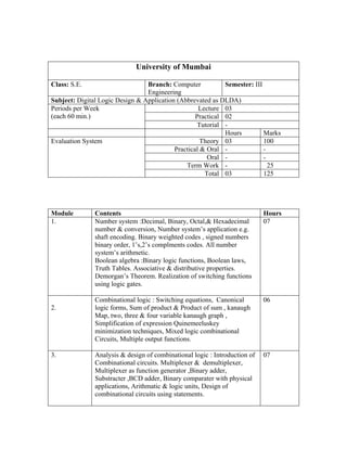
- 1. University of Mumbai Class: S.E. Branch: Computer Semester: III Engineering Subject: Digital Logic Design & Application (Abbrevated as DLDA) Periods per Week Lecture 03 (each 60 min.) Practical 02 Tutorial - Hours Marks Evaluation System Theory 03 100 Practical & Oral - - Oral - - Term Work - 25 Total 03 125 Module Contents Hours 1. Number system :Decimal, Binary, Octal,& Hexadecimal 07 number & conversion, Number system’s application e.g. shaft encoding. Binary weighted codes , signed numbers binary order, 1’s,2’s complments codes. All number system’s arithmetic. Boolean algebra :Binary logic functions, Boolean laws, Truth Tables. Associative & distributive properties. Demorgan’s Theorem. Realization of switching functions using logic gates. Combinational logic : Switching equations, Canonical 06 2. logic forms, Sum of product & Product of sum , kanaugh Map, two, three & four variable kanaugh graph , Simplification of expression Quinemeeluskey minimization techniques, Mixed logic combinational Circuits, Multiple output functions. 3. Analysis & design of combinational logic : Introduction of 07 Combinational circuits. Multiplexer & demultiplexer, Multiplexer as function generator ,Binary adder, Substracter ,BCD adder, Binary comparater with physical applications, Arithmatic & logic units, Design of combinational circuits using statements.
- 2. 4. Sequential Logic : Sequential circuits, Flip-Flop 05 conversions, Clocked & edge triggered flip flops timing specification, Timing analysis, state diagrams & tables, transition tables, Excitation table & equation ,examples using statement. 5. Sequential Circuits: Simple synchronous & asynchronous 06 Sequential Circuits analysis, Different types of counters asynchronous & synchronous, Counter Design with state equations, Registers, Different types of Shift register, Construction of state diagram & counter design. 6. Digital integrated circuits: Digital circuit logic levels, 05 propagation delay times, power dissipation ,Fan out & Fan in. Noise margin for popular logic families. TTL ,TTI sub families. CMOS & their performance comparison ( Numerical expeeted) Term work 1. Term work should consist of at least 8 practical experiment duly graded(Desirable 10 experiment) & two assignments covering all the topics of the syllabus. 2. A term work test must be conducted with a weightage of 10 marks covering complete syllabus. List of experiment: 1. Study of Basic Gates & universal gates. 2 .Realization of logical expression using Universal Gates& Basic gates. 3. Binary Arithmatic circuits 1)Adder 2) Substracter. 4. Implement certain function using multiplexer [16:1 ,8:1 ,4:1 ] 5. Design & implement 4:1 multiplexer with strobe 1/p active low using NAND & NOR Gate. 6. To design & implement any one code converter [e.g. Exess-3,BCD—Gray] Using Decoder & demultiplexer. 7. To design & implement 4=bit parity generator /checker using
- 3. 1) Minimum number of gates . 2) IC 74180. 8. Design of 7-segment display using decoder [IC 7447] 9. Design of JK Flip flop using NAND Gates & verification of the same flip flop Using IC7476. 10. Design of asynchronous up & Down counter. 11. Design of synchronous Counter. 12. Design of randam sequence generator. 13. Design of shift register using flip-flop verification of different modes. 14. verification of function table of universal shift register IC 74194. 15. Compare propagation delay & transfer characterstics of TTL & CMOS gates [use odd no. of gates] Text Books: 1. R. P. jain ,”Modern Digital Eletronics”, Tata McGraw Hill. 2. John F.Warrly, ”Digital Design Principal & Practices”, Pearson Education ,Russia. 3. M ..Morris Mano, “Digital Logic & computer Design”, PHI Reference Books: 1.John M . yarbrough ,”Digital Logic ”Thomson Learing. 2.Samual Lee ,”Digital Circuits & Logic Design “,PHI. 3.Carles H. Roth, “Fundamental of Logic Design,(4thedition ),junior jaico Book.