SlideShare ist ein Scribd-Unternehmen logo
1 von 20
Pin Description of Intel 8086
Microprocessor
1
8086 was the first 16-bit microprocessor available in 40-pin
DIP (Dual Inline Package) chip.
2
Intel 8086 MP can operate in two modes
• minimum mode
• maximum mode
For Minimum mode, a unique processor system with a single 8086
is required.
For Maximum mode a multiprocessor system with more than one
8086 is required.
3
Power supply and frequency signals:
It uses 5V DC supply at VCC pin 40, and uses ground at VSS pin 1 and 20 for
its operation.
Clock signal:
Clock signal is provided through Pin-19.
It provides timing to the processor for operations. Its frequency is
different for different versions, i.e. 5MHz, 8MHz and 10MHz.
Address/data bus: Pin 2-16
AD0-AD15 - These are 16 bit multiplexed address/data bus.
AD0-AD7 - carries low order byte data and
AD8-AD15 - carries higher order byte data.
During the first clock cycle, it carries 16-bit address and after that it
carries 16-bit data.
Address/status bus: Pin 35-38
A16-A19/S3-S6 -These are the 4 bit address/status buses. During the first
clock cycle, it carries 4-bit address and later it carries status signals.
4
S7/BHE:
BHE stands for Bus High Enable. It is available at pin 34 and it is used in
conjunction with AD0 to select the memory.
RD:
It is available at pin 32 and is used to read signal for Read operation.
Ready:
It is available at pin 32. It is an acknowledgement signal from I/O devices
that data is transferred. It is an active high signal. When it is high, it
indicates that the device is ready to transfer data. When it is low, it
indicates wait state.
RESET:
It is available at pin 21 and is used to restart the execution.
INTR:
It is available at pin 18. It is an interrupt request signal.
NMI:
It stands for non-maskable interrupt and is available at pin 17. It is an edge
triggered input, which causes an interrupt request to the microprocessor. 5
TEST:
This signal is like wait or idle state and is available at pin 23.
MN/MX:
It stands for Minimum/Maximum and is available at pin 33. when it is
high, it works in the minimum mode and vice-versa.
INTA:
It is an interrupt acknowledgement signal and available at pin 24.
When the microprocessor receives this signal, it acknowledges the
interrupt.
ALE: Address Latch Enable (Pin 25)
An o/p signal used to de-multiplexed AD0 to AD15 into A10 to A15 and
D0 to D15.
DEN:
It stands for Data Enable and is available at pin 26. It is used to enable
transceiver to separate data from the address / data bus.
6
DT/R:
It stands for Data Transmit / Receive signal and is available at pin 27. It
decides the direction of data flow through the transceiver.
M/IO
This signal is used to distinguish between memory and I/O operations.
When it is high, it indicates I/O operation and when it is low indicates the
memory operation. It is available at pin 28.
WR:
It stands for write signal and is available at pin 29.
It is used to write the data into the memory or the output device
depending on the status of M/IO signal.
HLDA:
It stands for Hold Acknowledgement signal and is available at pin 30. This
signal acknowledges the HOLD signal.
HOLD:
This signal indicates to the processor that external devices are requesting
to access the address/data buses. It is available at pin 31. 7
QS1 and QS0
These are queue status signals and are available at pin 24 and 25. These
signals provide the status of instruction queue.
Their conditions are shown in the following table,
S0, S1, S2
These are the status signals that provide the status of operation, which is
used by the Bus Controller 8288 to generate memory & I/O control
signals. These are available at pin 26, 27, and 28.
QS0 QS1 Status
0 0 No operation
0 1 First byte of opcode from the queue
1 0 Empty the queue
1 1 Subsequent byte from the queue
8
S2 S1 S0 Status
0 0 0 Interrupt acknowledgement
0 0 1 I/O Read
0 1 0 I/O Write
0 1 1 Halt
1 0 0 Opcode fetch
1 0 1 Memory read
1 1 0 Memory write
1 1 1 Passive state
9
LOCK:
This signal is used to lock the peripherals from the system . It is available
at pin 29.
RQ/GT1 and RQ/GT0
These are the Request/Grant signals used by the other processors
requesting the CPU to release the system bus.
When the signal is received by CPU, then it sends acknowledgment.
RQ/GT0 has a higher priority than RQ/GT1.
10
Register Organization of 8086
11
Intel 8086 uses 20 bit address lines. So its memory capacity is (2^20) =
1MB of memory. Memory segmentation is first introduced in this type
of microprocessor.
All the registers of 8086 are 16-bit registers. The general purpose
registers can be used as either 8-bit registers or 16-bit registers.
The register set of 8086 can be categorized into 4 different groups.
 General data registers
 Segment registers
 Pointers and index registers
 Status registers
12
General data registers
The registers AX, BX,CX and DX are the general purpose 16-bit registers.
AX is used as 16-bit accumulator.
Accumulator can be used for I/O operations, rotate and string
manipulation.
The lower 8-bit is designated as AL (accumulator) and higher 8-bit is
designated as AH.
BX is a 16 bit register mainly used as base register for memory address
calculation, BL indicates the lower 8-bit and BH indicates the higher 8-bit
of BX.
Register CX is used default counter (looping)
DX is used to hold I/O address during certain I/O instructions. Ex: If the
result of multiplication is more than 16 bits the low order bits are stored
in AX, the high-order 16 bits are stored in DX register. 13
Segment Registers
Intel 8086 is byte organized. Here 1 MB of memory is divided into 16
logical segments. Each segment contains 64 kilobytes of memory.
There are four segment register in 8086
• Code segment register (CS)
• Data segment register (DS)
• Extra segment register (ES)
• Stack segment register (SS)
Code segment register (CS): is used fro addressing memory location in the
code segment of the memory, where the executable program is stored.
Data segment register (DS): points to the data segment of the memory
where the data is stored.
Extra Segment Register (ES) : also refers to a segment in the memory
which is another data segment in the memory.
14
Stack Segment Registers:
• By default, the processor assumes that all data referenced by the stack
pointer (SP) and base pointer (BP) registers is located in the stack
segment.
• SS register can be changed directly using POP instruction.
• It is used for addressing stack segment of memory, which is used to
store stack data.
15
Pointers and Index Registers
The pointers IP, BP, SP usually contain offsets within the code, data and
stack segments respectively.
• Stack Pointer (SP) is a 16-bit register pointing to program stack in stack
segment.
• Base Pointer (BP) is a 16-bit register pointing to data in stack segment.
BP register is usually used for based indexed or register indirect
addressing.
The index registers are particularly useful for string manipulation.
SI is used to store the offset of source data in data segment.
DI is used to store the offset of destination in data or extra segment.
16
Status Register
It determines the current state of the processor. They are modified
automatically by CPU after mathematical operations, this allows to
determine the type of the result, and to determine conditions to
transfer control to other parts of the program.
Two types,
Conditional (or) Status Flag and Control Flag.
17
18
024
67
Status flag
Carry flag (CY)
It is set whenever there is a carry or borrow out of the MSB of a result.
CY=1, Carry is generated
CY=0, Carry is not generated
Parity flag (PF)
It is set if the result has even parity. If parity is odd, PF is reset.
Auxiliary carry flag (AC)
Holds a carry after addition or a borrow after subtraction between bit
positions 3 and 4 of the result.
Zero flag (ZF)
Indicates that the result of an arithmetic or logic operation It is set if
the result is zero
Sign flag (SF)
Indicates the arithmetic sign of the result after an addition or
subtraction. If S = 1, the result is negative. If S = 0, the result is positive.19
Overflow flag (OF)
A overflow condition indicates that a result has exceeded the capacity of
the machine. A condition that can occur when signed numbers are added
or subtracted.
Control Flags
Trap flag (TF)
Debugging feature of the microprocessor
Interrupt enable flag (IF) - interrupt controls operation
If I = 1, the INTR pin is enabled. If I = 0, the INTR pin is disabled.
Direction flag (DF)
Controls the selection of increment and decrement for the DI and SI
registers during string instructions.
20

Weitere ähnliche Inhalte

Was ist angesagt?

Architecture of 8051 microcontroller))
Architecture of 8051 microcontroller))Architecture of 8051 microcontroller))
Architecture of 8051 microcontroller))
Ganesh Ram
 
Minimum Modes and Maximum Modes of 8086 Microprocessor
Minimum Modes and Maximum Modes of 8086 MicroprocessorMinimum Modes and Maximum Modes of 8086 Microprocessor
Minimum Modes and Maximum Modes of 8086 Microprocessor
Nikhil Kumar
 
8237 dma controller
8237 dma controller8237 dma controller
8237 dma controller
Tech_MX
 
Chapter 2 The 8088 Microprocessor
Chapter 2   The 8088 MicroprocessorChapter 2   The 8088 Microprocessor
Chapter 2 The 8088 Microprocessor
Dwight Sabio
 

Was ist angesagt? (20)

Introduction to pic microcontroller
Introduction to pic microcontrollerIntroduction to pic microcontroller
Introduction to pic microcontroller
 
Architecture of 8051 microcontroller))
Architecture of 8051 microcontroller))Architecture of 8051 microcontroller))
Architecture of 8051 microcontroller))
 
8259 Programmable Interrupt Controller
8259 Programmable Interrupt Controller8259 Programmable Interrupt Controller
8259 Programmable Interrupt Controller
 
30. 8086 microprocessor pipelined architecture
30. 8086 microprocessor pipelined architecture30. 8086 microprocessor pipelined architecture
30. 8086 microprocessor pipelined architecture
 
80286 microprocessor
80286 microprocessor80286 microprocessor
80286 microprocessor
 
Minimum Modes and Maximum Modes of 8086 Microprocessor
Minimum Modes and Maximum Modes of 8086 MicroprocessorMinimum Modes and Maximum Modes of 8086 Microprocessor
Minimum Modes and Maximum Modes of 8086 Microprocessor
 
8086
8086 8086
8086
 
8085 microprocessor ramesh gaonkar
8085 microprocessor   ramesh gaonkar8085 microprocessor   ramesh gaonkar
8085 microprocessor ramesh gaonkar
 
8086 pin diagram description
8086 pin diagram description8086 pin diagram description
8086 pin diagram description
 
8259 Programmable Interrupt Controller by vijay
8259 Programmable Interrupt Controller by vijay8259 Programmable Interrupt Controller by vijay
8259 Programmable Interrupt Controller by vijay
 
Interrupts of microprocessor 8085
Interrupts of microprocessor  8085Interrupts of microprocessor  8085
Interrupts of microprocessor 8085
 
8237 dma controller
8237 dma controller8237 dma controller
8237 dma controller
 
Motorola microprocessor
Motorola microprocessorMotorola microprocessor
Motorola microprocessor
 
Chapter 2 The 8088 Microprocessor
Chapter 2   The 8088 MicroprocessorChapter 2   The 8088 Microprocessor
Chapter 2 The 8088 Microprocessor
 
8086 class notes-Y.N.M
8086 class notes-Y.N.M8086 class notes-Y.N.M
8086 class notes-Y.N.M
 
Assembler directives and basic steps ALP of 8086
Assembler directives and basic steps ALP of 8086Assembler directives and basic steps ALP of 8086
Assembler directives and basic steps ALP of 8086
 
PIC Microcontrollers
PIC MicrocontrollersPIC Microcontrollers
PIC Microcontrollers
 
8086 pin details
8086 pin details8086 pin details
8086 pin details
 
8086 micro processor
8086 micro processor8086 micro processor
8086 micro processor
 
Intel 80486 Microprocessor
Intel 80486 MicroprocessorIntel 80486 Microprocessor
Intel 80486 Microprocessor
 

Ähnlich wie Pin Description and Register Organization of 8086 Microprocessor

Microprocessors and microcontrollers
Microprocessors and microcontrollersMicroprocessors and microcontrollers
Microprocessors and microcontrollers
gomathy S
 
Microprocessor and microcontroller
Microprocessor and microcontrollerMicroprocessor and microcontroller
Microprocessor and microcontroller
Ravinder Singla
 

Ähnlich wie Pin Description and Register Organization of 8086 Microprocessor (20)

unit 4 mc.pdf
unit 4 mc.pdfunit 4 mc.pdf
unit 4 mc.pdf
 
microprocessor_part_3_compressed_1588259301.pdf
microprocessor_part_3_compressed_1588259301.pdfmicroprocessor_part_3_compressed_1588259301.pdf
microprocessor_part_3_compressed_1588259301.pdf
 
Microprocessors and microcontrollers
Microprocessors and microcontrollersMicroprocessors and microcontrollers
Microprocessors and microcontrollers
 
8086 new
8086 new8086 new
8086 new
 
8086 complete guide
8086 complete guide 8086 complete guide
8086 complete guide
 
mic_unit1.pdf msbte unit 1 note pdf in ppt
mic_unit1.pdf msbte unit 1 note pdf in pptmic_unit1.pdf msbte unit 1 note pdf in ppt
mic_unit1.pdf msbte unit 1 note pdf in ppt
 
8085_LAB_PROGRAMS.pdf
8085_LAB_PROGRAMS.pdf8085_LAB_PROGRAMS.pdf
8085_LAB_PROGRAMS.pdf
 
pin-diagram-details-of-8086-microprocessor
pin-diagram-details-of-8086-microprocessorpin-diagram-details-of-8086-microprocessor
pin-diagram-details-of-8086-microprocessor
 
Microprocessor 8086
Microprocessor 8086Microprocessor 8086
Microprocessor 8086
 
janakiraman egsp collage I msc 4 unit
janakiraman egsp collage  I msc 4 unitjanakiraman egsp collage  I msc 4 unit
janakiraman egsp collage I msc 4 unit
 
Mpmc
MpmcMpmc
Mpmc
 
janakiraman I msc 4 unit
janakiraman I msc 4 unitjanakiraman I msc 4 unit
janakiraman I msc 4 unit
 
8086
80868086
8086
 
Microprocessor 8086
Microprocessor 8086Microprocessor 8086
Microprocessor 8086
 
Microprocessor 8085 architecture ppt. april 2013
Microprocessor 8085 architecture ppt. april 2013Microprocessor 8085 architecture ppt. april 2013
Microprocessor 8085 architecture ppt. april 2013
 
Introduction to 8085 Microprocessor
Introduction to 8085 MicroprocessorIntroduction to 8085 Microprocessor
Introduction to 8085 Microprocessor
 
8085 architecture
8085 architecture8085 architecture
8085 architecture
 
Microprocessor and microcontroller
Microprocessor and microcontrollerMicroprocessor and microcontroller
Microprocessor and microcontroller
 
8085 microprocessor Architecture and Pin description
8085 microprocessor Architecture and Pin description 8085 microprocessor Architecture and Pin description
8085 microprocessor Architecture and Pin description
 
Microprocessor
Microprocessor Microprocessor
Microprocessor
 

Kürzlich hochgeladen

1029 - Danh muc Sach Giao Khoa 10 . pdf
1029 -  Danh muc Sach Giao Khoa 10 . pdf1029 -  Danh muc Sach Giao Khoa 10 . pdf
1029 - Danh muc Sach Giao Khoa 10 . pdf
QucHHunhnh
 
Activity 01 - Artificial Culture (1).pdf
Activity 01 - Artificial Culture (1).pdfActivity 01 - Artificial Culture (1).pdf
Activity 01 - Artificial Culture (1).pdf
ciinovamais
 
Jual Obat Aborsi Hongkong ( Asli No.1 ) 085657271886 Obat Penggugur Kandungan...
Jual Obat Aborsi Hongkong ( Asli No.1 ) 085657271886 Obat Penggugur Kandungan...Jual Obat Aborsi Hongkong ( Asli No.1 ) 085657271886 Obat Penggugur Kandungan...
Jual Obat Aborsi Hongkong ( Asli No.1 ) 085657271886 Obat Penggugur Kandungan...
ZurliaSoop
 

Kürzlich hochgeladen (20)

Third Battle of Panipat detailed notes.pptx
Third Battle of Panipat detailed notes.pptxThird Battle of Panipat detailed notes.pptx
Third Battle of Panipat detailed notes.pptx
 
This PowerPoint helps students to consider the concept of infinity.
This PowerPoint helps students to consider the concept of infinity.This PowerPoint helps students to consider the concept of infinity.
This PowerPoint helps students to consider the concept of infinity.
 
Kodo Millet PPT made by Ghanshyam bairwa college of Agriculture kumher bhara...
Kodo Millet  PPT made by Ghanshyam bairwa college of Agriculture kumher bhara...Kodo Millet  PPT made by Ghanshyam bairwa college of Agriculture kumher bhara...
Kodo Millet PPT made by Ghanshyam bairwa college of Agriculture kumher bhara...
 
Mehran University Newsletter Vol-X, Issue-I, 2024
Mehran University Newsletter Vol-X, Issue-I, 2024Mehran University Newsletter Vol-X, Issue-I, 2024
Mehran University Newsletter Vol-X, Issue-I, 2024
 
Mixin Classes in Odoo 17 How to Extend Models Using Mixin Classes
Mixin Classes in Odoo 17  How to Extend Models Using Mixin ClassesMixin Classes in Odoo 17  How to Extend Models Using Mixin Classes
Mixin Classes in Odoo 17 How to Extend Models Using Mixin Classes
 
Application orientated numerical on hev.ppt
Application orientated numerical on hev.pptApplication orientated numerical on hev.ppt
Application orientated numerical on hev.ppt
 
SKILL OF INTRODUCING THE LESSON MICRO SKILLS.pptx
SKILL OF INTRODUCING THE LESSON MICRO SKILLS.pptxSKILL OF INTRODUCING THE LESSON MICRO SKILLS.pptx
SKILL OF INTRODUCING THE LESSON MICRO SKILLS.pptx
 
1029 - Danh muc Sach Giao Khoa 10 . pdf
1029 -  Danh muc Sach Giao Khoa 10 . pdf1029 -  Danh muc Sach Giao Khoa 10 . pdf
1029 - Danh muc Sach Giao Khoa 10 . pdf
 
Making communications land - Are they received and understood as intended? we...
Making communications land - Are they received and understood as intended? we...Making communications land - Are they received and understood as intended? we...
Making communications land - Are they received and understood as intended? we...
 
On National Teacher Day, meet the 2024-25 Kenan Fellows
On National Teacher Day, meet the 2024-25 Kenan FellowsOn National Teacher Day, meet the 2024-25 Kenan Fellows
On National Teacher Day, meet the 2024-25 Kenan Fellows
 
Activity 01 - Artificial Culture (1).pdf
Activity 01 - Artificial Culture (1).pdfActivity 01 - Artificial Culture (1).pdf
Activity 01 - Artificial Culture (1).pdf
 
How to Manage Global Discount in Odoo 17 POS
How to Manage Global Discount in Odoo 17 POSHow to Manage Global Discount in Odoo 17 POS
How to Manage Global Discount in Odoo 17 POS
 
TỔNG ÔN TẬP THI VÀO LỚP 10 MÔN TIẾNG ANH NĂM HỌC 2023 - 2024 CÓ ĐÁP ÁN (NGỮ Â...
TỔNG ÔN TẬP THI VÀO LỚP 10 MÔN TIẾNG ANH NĂM HỌC 2023 - 2024 CÓ ĐÁP ÁN (NGỮ Â...TỔNG ÔN TẬP THI VÀO LỚP 10 MÔN TIẾNG ANH NĂM HỌC 2023 - 2024 CÓ ĐÁP ÁN (NGỮ Â...
TỔNG ÔN TẬP THI VÀO LỚP 10 MÔN TIẾNG ANH NĂM HỌC 2023 - 2024 CÓ ĐÁP ÁN (NGỮ Â...
 
PROCESS RECORDING FORMAT.docx
PROCESS      RECORDING        FORMAT.docxPROCESS      RECORDING        FORMAT.docx
PROCESS RECORDING FORMAT.docx
 
Holdier Curriculum Vitae (April 2024).pdf
Holdier Curriculum Vitae (April 2024).pdfHoldier Curriculum Vitae (April 2024).pdf
Holdier Curriculum Vitae (April 2024).pdf
 
Jual Obat Aborsi Hongkong ( Asli No.1 ) 085657271886 Obat Penggugur Kandungan...
Jual Obat Aborsi Hongkong ( Asli No.1 ) 085657271886 Obat Penggugur Kandungan...Jual Obat Aborsi Hongkong ( Asli No.1 ) 085657271886 Obat Penggugur Kandungan...
Jual Obat Aborsi Hongkong ( Asli No.1 ) 085657271886 Obat Penggugur Kandungan...
 
Unit-IV; Professional Sales Representative (PSR).pptx
Unit-IV; Professional Sales Representative (PSR).pptxUnit-IV; Professional Sales Representative (PSR).pptx
Unit-IV; Professional Sales Representative (PSR).pptx
 
Introduction to Nonprofit Accounting: The Basics
Introduction to Nonprofit Accounting: The BasicsIntroduction to Nonprofit Accounting: The Basics
Introduction to Nonprofit Accounting: The Basics
 
Dyslexia AI Workshop for Slideshare.pptx
Dyslexia AI Workshop for Slideshare.pptxDyslexia AI Workshop for Slideshare.pptx
Dyslexia AI Workshop for Slideshare.pptx
 
Food safety_Challenges food safety laboratories_.pdf
Food safety_Challenges food safety laboratories_.pdfFood safety_Challenges food safety laboratories_.pdf
Food safety_Challenges food safety laboratories_.pdf
 

Pin Description and Register Organization of 8086 Microprocessor

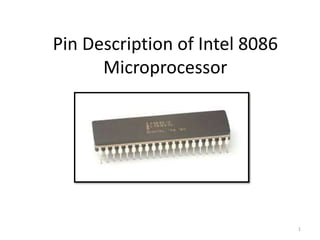
  • 1. Pin Description of Intel 8086 Microprocessor 1
  • 2. 8086 was the first 16-bit microprocessor available in 40-pin DIP (Dual Inline Package) chip. 2
  • 3. Intel 8086 MP can operate in two modes • minimum mode • maximum mode For Minimum mode, a unique processor system with a single 8086 is required. For Maximum mode a multiprocessor system with more than one 8086 is required. 3
  • 4. Power supply and frequency signals: It uses 5V DC supply at VCC pin 40, and uses ground at VSS pin 1 and 20 for its operation. Clock signal: Clock signal is provided through Pin-19. It provides timing to the processor for operations. Its frequency is different for different versions, i.e. 5MHz, 8MHz and 10MHz. Address/data bus: Pin 2-16 AD0-AD15 - These are 16 bit multiplexed address/data bus. AD0-AD7 - carries low order byte data and AD8-AD15 - carries higher order byte data. During the first clock cycle, it carries 16-bit address and after that it carries 16-bit data. Address/status bus: Pin 35-38 A16-A19/S3-S6 -These are the 4 bit address/status buses. During the first clock cycle, it carries 4-bit address and later it carries status signals. 4
  • 5. S7/BHE: BHE stands for Bus High Enable. It is available at pin 34 and it is used in conjunction with AD0 to select the memory. RD: It is available at pin 32 and is used to read signal for Read operation. Ready: It is available at pin 32. It is an acknowledgement signal from I/O devices that data is transferred. It is an active high signal. When it is high, it indicates that the device is ready to transfer data. When it is low, it indicates wait state. RESET: It is available at pin 21 and is used to restart the execution. INTR: It is available at pin 18. It is an interrupt request signal. NMI: It stands for non-maskable interrupt and is available at pin 17. It is an edge triggered input, which causes an interrupt request to the microprocessor. 5
  • 6. TEST: This signal is like wait or idle state and is available at pin 23. MN/MX: It stands for Minimum/Maximum and is available at pin 33. when it is high, it works in the minimum mode and vice-versa. INTA: It is an interrupt acknowledgement signal and available at pin 24. When the microprocessor receives this signal, it acknowledges the interrupt. ALE: Address Latch Enable (Pin 25) An o/p signal used to de-multiplexed AD0 to AD15 into A10 to A15 and D0 to D15. DEN: It stands for Data Enable and is available at pin 26. It is used to enable transceiver to separate data from the address / data bus. 6
  • 7. DT/R: It stands for Data Transmit / Receive signal and is available at pin 27. It decides the direction of data flow through the transceiver. M/IO This signal is used to distinguish between memory and I/O operations. When it is high, it indicates I/O operation and when it is low indicates the memory operation. It is available at pin 28. WR: It stands for write signal and is available at pin 29. It is used to write the data into the memory or the output device depending on the status of M/IO signal. HLDA: It stands for Hold Acknowledgement signal and is available at pin 30. This signal acknowledges the HOLD signal. HOLD: This signal indicates to the processor that external devices are requesting to access the address/data buses. It is available at pin 31. 7
  • 8. QS1 and QS0 These are queue status signals and are available at pin 24 and 25. These signals provide the status of instruction queue. Their conditions are shown in the following table, S0, S1, S2 These are the status signals that provide the status of operation, which is used by the Bus Controller 8288 to generate memory & I/O control signals. These are available at pin 26, 27, and 28. QS0 QS1 Status 0 0 No operation 0 1 First byte of opcode from the queue 1 0 Empty the queue 1 1 Subsequent byte from the queue 8
  • 9. S2 S1 S0 Status 0 0 0 Interrupt acknowledgement 0 0 1 I/O Read 0 1 0 I/O Write 0 1 1 Halt 1 0 0 Opcode fetch 1 0 1 Memory read 1 1 0 Memory write 1 1 1 Passive state 9
  • 10. LOCK: This signal is used to lock the peripherals from the system . It is available at pin 29. RQ/GT1 and RQ/GT0 These are the Request/Grant signals used by the other processors requesting the CPU to release the system bus. When the signal is received by CPU, then it sends acknowledgment. RQ/GT0 has a higher priority than RQ/GT1. 10
  • 12. Intel 8086 uses 20 bit address lines. So its memory capacity is (2^20) = 1MB of memory. Memory segmentation is first introduced in this type of microprocessor. All the registers of 8086 are 16-bit registers. The general purpose registers can be used as either 8-bit registers or 16-bit registers. The register set of 8086 can be categorized into 4 different groups.  General data registers  Segment registers  Pointers and index registers  Status registers 12
  • 13. General data registers The registers AX, BX,CX and DX are the general purpose 16-bit registers. AX is used as 16-bit accumulator. Accumulator can be used for I/O operations, rotate and string manipulation. The lower 8-bit is designated as AL (accumulator) and higher 8-bit is designated as AH. BX is a 16 bit register mainly used as base register for memory address calculation, BL indicates the lower 8-bit and BH indicates the higher 8-bit of BX. Register CX is used default counter (looping) DX is used to hold I/O address during certain I/O instructions. Ex: If the result of multiplication is more than 16 bits the low order bits are stored in AX, the high-order 16 bits are stored in DX register. 13
  • 14. Segment Registers Intel 8086 is byte organized. Here 1 MB of memory is divided into 16 logical segments. Each segment contains 64 kilobytes of memory. There are four segment register in 8086 • Code segment register (CS) • Data segment register (DS) • Extra segment register (ES) • Stack segment register (SS) Code segment register (CS): is used fro addressing memory location in the code segment of the memory, where the executable program is stored. Data segment register (DS): points to the data segment of the memory where the data is stored. Extra Segment Register (ES) : also refers to a segment in the memory which is another data segment in the memory. 14
  • 15. Stack Segment Registers: • By default, the processor assumes that all data referenced by the stack pointer (SP) and base pointer (BP) registers is located in the stack segment. • SS register can be changed directly using POP instruction. • It is used for addressing stack segment of memory, which is used to store stack data. 15
  • 16. Pointers and Index Registers The pointers IP, BP, SP usually contain offsets within the code, data and stack segments respectively. • Stack Pointer (SP) is a 16-bit register pointing to program stack in stack segment. • Base Pointer (BP) is a 16-bit register pointing to data in stack segment. BP register is usually used for based indexed or register indirect addressing. The index registers are particularly useful for string manipulation. SI is used to store the offset of source data in data segment. DI is used to store the offset of destination in data or extra segment. 16
  • 17. Status Register It determines the current state of the processor. They are modified automatically by CPU after mathematical operations, this allows to determine the type of the result, and to determine conditions to transfer control to other parts of the program. Two types, Conditional (or) Status Flag and Control Flag. 17
  • 19. Status flag Carry flag (CY) It is set whenever there is a carry or borrow out of the MSB of a result. CY=1, Carry is generated CY=0, Carry is not generated Parity flag (PF) It is set if the result has even parity. If parity is odd, PF is reset. Auxiliary carry flag (AC) Holds a carry after addition or a borrow after subtraction between bit positions 3 and 4 of the result. Zero flag (ZF) Indicates that the result of an arithmetic or logic operation It is set if the result is zero Sign flag (SF) Indicates the arithmetic sign of the result after an addition or subtraction. If S = 1, the result is negative. If S = 0, the result is positive.19
  • 20. Overflow flag (OF) A overflow condition indicates that a result has exceeded the capacity of the machine. A condition that can occur when signed numbers are added or subtracted. Control Flags Trap flag (TF) Debugging feature of the microprocessor Interrupt enable flag (IF) - interrupt controls operation If I = 1, the INTR pin is enabled. If I = 0, the INTR pin is disabled. Direction flag (DF) Controls the selection of increment and decrement for the DI and SI registers during string instructions. 20