SlideShare ist ein Scribd-Unternehmen logo
1 von 6
Department of Electrical Engineering
Faculty of Engineering & Applied Sciences
Riphah International University, Islamabad, Pakistan
Program: B.Sc. Electrical Engineering Semester: III
Subject EE-241 Basic Electronics Date: …………….
Experiment 1: To obtain the V-I characteristics of PN junction diode
OBJECTIVES:
(i) To understand the concept and working of PN junction diode.
(ii) To obtain V-I characteristics of PN junction diode.
Name : Roll no:
Performance Lab Report
Description Total
Marks
Marks
Obtained
Description Total
Marks
Marks
Obtained
Ability to
conduct
Experiment
5 Organization/Structure 5
Data Analysis &
Interpretation
5 Calculation & Data
Presentation
5
Total Marks obtained
Remarks (if any): ………………………………….
Name & Signature of faculty: …………………………………
Introduction:
The semiconductor diode is formed by doping P-type impurity in one side and N-
type of impurity in another side of the semiconductor crystal forming a p-n junction
as shown in the following figure.
At the junction initially free charge carriers from both side recombine forming
negatively charged ions in P side of junction (an atom in P -side accept electron and
becomes negatively charged ion) and positively charged ion on n side(an atom in n-
side accepts hole i.e. donates electron and becomes positively charged ion)region.
This region deplete of any type of free charge carrier is called as depletion region.
Further recombination of free carrier on both sides is prevented because of the
depletion voltage generated due to charge carriers kept at distance by depletion
(acts as a sort of insulation) layer as shown dotted in the above figure.
Working principle:
When voltage is not applied across the diode, depletion region forms as shown in
the above figure. When the voltage is applied between the two terminals of the diode
(anode and cathode) two possibilities arises depending on polarity of DC supply.
1. Forward-Bias Condition: When the +Ve terminal of the battery is connected to
P-type material & -Ve terminal to N-type terminal as shown in the circuit diagram,
the diode is said to be forward biased. The application of forward bias voltage will
force electrons in N-type and holes in P-type material to recombine with the ions
near boundary and to flow crossing junction. This reduces width of depletion
region. This further will result in increase in majority carriers flow across the
junction. If forward bias is further increased in magnitude the depletion region
width will continue to decrease resulting in exponential rise in current as in ideal
diode characteristic curve.
2. Reverse-biased: If the negative terminal of battery (DC power supply) is
connected with P-type terminal of diode and +Ve terminal of battery connected to
N type then diode is said to be reverse biased. In this condition the free charge
carriers (i.e. electrons in N-type and holes in P-type) will move away from
junction widening depletion region width. The minority carriers (i.e. -ve electrons
in p-type and +ve holes in n-type) can cross the depletion region resulting in
minority carrier current flow called as reverse saturation current (Is). As no of
minority carrier is very small so the
magnitude of few microamperes. Ideally current in reverse bias is zero.
In short current flows through diode in forward bias, and does not flow through diode
in reverse bias. Diode can pass current only in one direction.
Experiment Procedure:
 Connect the power supply, voltmeter, current meter with the diode as shown in
the figure for forward bias diode. You can use two multimeter (one to measure
current through diode and other to measure voltage across diode) 
 Increase voltage from the power supply from 0V to 20V in step as shown
in the observation table 

 Measure voltage across diode and current through diode. Note down
readings in the observation table. 

 Reverse DC power supply polarity for reverse bias 

 Repeat the above procedure for the different values of supply voltage for 
reverse bias
Draw VI characteristics for forward bias and reverse bias in one graph
Circuit diagram (forward bias)
Circuit diagram (Reverse bias)
Observation table: (Forward bias)
Sr. Supply Diode Diode
No Voltage Voltage Current
(Volts) Vd Id
1 0.2 0.144 0
2 0.4 0.364 0
3 0.6 0.456 0.05
4 0.8 0.516 0.21
5 1.0 0.547 0.43
6 2.0 0.599 1.3
3.0 0.626 2.3
4.0 0.642 3.4
5.0 0.654 4.3
6.0 0.664 5.4
Observation table: (Reverse bias)
Sr. Supply Diode Diode
No Voltage Voltage Current
(Volts) Vd Id
1 0.2 0.12 0
2 0.4 0.36 0
3 0.6 0.54 0
4 0.8 0.72 0
5 1.0 0.89 0
6 2.0 1.93 0
3.0 2.99 0
4.0 3.99 0
5.0 4.99 0
6.0 5.93 0
Draw V-I characteristics of PN junction diode:
Questions:
[1] List important specifications of the diode
Ans: Specifications of Diode
 Maximum repetitive reverse voltage = 100 V.
 Average rectified forward current = 200 mA.
 Maximum direct forward current = 300 mA.
 Maximum forward voltage drop = 1.0 V at 10 mA.
 Non-repetitive peak forward surge current = 1.0 A (pulse width = 1 s)
 Total power dissipation = 500 MW.
[2] What is breakdown voltage? What is the breakdown voltage of diode 1N4001
and 1N4007?
Ans:. Breakdown Voltage: The breakdown voltage of an insulator is the
minimum voltage thatcauses a portion of an insulator to become electrically
conductive. For diodes, the breakdownvoltage is the minimum reverse voltage that
makes the diode conduct appreciably in reverse.1N4001 Diode will break down at
50 volts or less and 1N4007 diode will breakdown at1000V.
[3] List different types of the diode
Ans: Types of Diodes
Laser diode.
Avalanche diode.
Light Emitting Diode.
Zener diode.
Schottky diode.
Photodiode.
PN junction diode.
[5] How to check diode with help of multimeter?
Ans: Connect the red probe of the multimeter to the anode and black probe to the
cathode. This means the diode is forward-biased. Observe the reading on multimeter's
display. If the displayed voltage value is in between 0.6 to 0.7 (for a Silicon Diode), then
the diode is healthy and perfect
[6] What is the reason for reverse saturation current ?
Ans: The reverse saturation current is the part of the reverse current in a semiconductor
diode which is caused by the diffusion of minority carriers from the neutral regions to the
depletion region.
[7] What is the forward voltage drop of silicon diode and germanium diode?
Ans: Forward voltage for a diode varies only slightly for changes in forward current and
temperature, and is fixed by the chemical composition of the P-N junction. Silicon
diodes have a forward voltage of approximately 0.7 volts. Germanium diodes have a
forward voltage of approximately 0.3 volts.
Observations & Discussion
Whena diode isconnectedina ForwardBias condition,anegative voltage isappliedtothe
N-type material andapositive voltageisappliedtothe P-type material.Inthe forwardbiased
condition, the current varies with the voltage. When a diode is connected in a Reverse
Biascondition,apositive voltage isappliedtothe N-type material andanegative voltageis
appliedtothe P-type material.Inreversedbiasedconditionthe voltagesremainsame,butthe
currentis zeroat any point.This isdue the wide depletionregionthe smallcurrentflowsbut
itsalmostzeroand neglected.
Conclusion:
In today’s lab I learned about the diode, types of Diode its specifications and its
characteristics.Ialsolearnedaboutthe workingof the Diode,itsPN Junction,holes,and
electrons depletion region. I also learned about the Forward biased and Reverse biased
Conditionsof the diode.Ilearnedaboutthe interiorof the diode.

Weitere ähnliche Inhalte

Was ist angesagt?

Lecture trans bias_1
Lecture trans bias_1Lecture trans bias_1
Lecture trans bias_1Napex Terra
 
Chapter 2: Direct Current (DC) Circuits
Chapter 2: Direct Current (DC) CircuitsChapter 2: Direct Current (DC) Circuits
Chapter 2: Direct Current (DC) CircuitsJeremyLauKarHei
 
Diode voltage multiplier
Diode voltage multiplierDiode voltage multiplier
Diode voltage multiplierUnsa Shakir
 
Bjt amplifiers
Bjt amplifiersBjt amplifiers
Bjt amplifiersGastarot
 
EST 130, Transistor Biasing and Amplification.
EST 130, Transistor Biasing and Amplification.EST 130, Transistor Biasing and Amplification.
EST 130, Transistor Biasing and Amplification.CKSunith1
 
Chapter 3: AC Sources and AC Characteristic
Chapter 3: AC Sources and AC CharacteristicChapter 3: AC Sources and AC Characteristic
Chapter 3: AC Sources and AC CharacteristicJeremyLauKarHei
 
Lab 8 bipolar junction transistor characterstics
Lab 8  bipolar junction transistor charactersticsLab 8  bipolar junction transistor characterstics
Lab 8 bipolar junction transistor charactersticskehali Haileselassie
 
Hybrid model for Transistor, small signal Analysis
Hybrid model for Transistor, small signal AnalysisHybrid model for Transistor, small signal Analysis
Hybrid model for Transistor, small signal AnalysisAbhishek Choksi
 
Physics Class 12 Powerpoint presentation
Physics Class 12 Powerpoint presentationPhysics Class 12 Powerpoint presentation
Physics Class 12 Powerpoint presentationBibin Vincent
 
Semiconductor basics
Semiconductor basicsSemiconductor basics
Semiconductor basicsRohit Kumar
 
Mba admssion in india
Mba admssion in indiaMba admssion in india
Mba admssion in indiaEdhole.com
 
EST 130, PN Junction Diodes
EST 130, PN Junction DiodesEST 130, PN Junction Diodes
EST 130, PN Junction DiodesCKSunith1
 

Was ist angesagt? (20)

Cbcs b sc i sem e1 unit 1
Cbcs b sc i sem e1 unit 1Cbcs b sc i sem e1 unit 1
Cbcs b sc i sem e1 unit 1
 
Lecture trans bias_1
Lecture trans bias_1Lecture trans bias_1
Lecture trans bias_1
 
Bsc 1 cbcs e1 unit 2
Bsc 1 cbcs e1 unit 2Bsc 1 cbcs e1 unit 2
Bsc 1 cbcs e1 unit 2
 
Diodes vi characteries
Diodes vi characteriesDiodes vi characteries
Diodes vi characteries
 
Cbcs e1 unit 3
Cbcs e1 unit 3Cbcs e1 unit 3
Cbcs e1 unit 3
 
207137236 ee2207-lm
207137236 ee2207-lm207137236 ee2207-lm
207137236 ee2207-lm
 
Chapter 2: Direct Current (DC) Circuits
Chapter 2: Direct Current (DC) CircuitsChapter 2: Direct Current (DC) Circuits
Chapter 2: Direct Current (DC) Circuits
 
Diode voltage multiplier
Diode voltage multiplierDiode voltage multiplier
Diode voltage multiplier
 
EC6202 ELECTRONIC DEVICES AND CIRCUITS Unit 2
EC6202 ELECTRONIC DEVICES AND CIRCUITS Unit 2EC6202 ELECTRONIC DEVICES AND CIRCUITS Unit 2
EC6202 ELECTRONIC DEVICES AND CIRCUITS Unit 2
 
EC6202 ELECTRONIC DEVICES AND CIRCUITS NOTES
EC6202 ELECTRONIC DEVICES AND CIRCUITS NOTESEC6202 ELECTRONIC DEVICES AND CIRCUITS NOTES
EC6202 ELECTRONIC DEVICES AND CIRCUITS NOTES
 
Bjt amplifiers
Bjt amplifiersBjt amplifiers
Bjt amplifiers
 
EST 130, Transistor Biasing and Amplification.
EST 130, Transistor Biasing and Amplification.EST 130, Transistor Biasing and Amplification.
EST 130, Transistor Biasing and Amplification.
 
Chapter 3: AC Sources and AC Characteristic
Chapter 3: AC Sources and AC CharacteristicChapter 3: AC Sources and AC Characteristic
Chapter 3: AC Sources and AC Characteristic
 
B sc i cbcs unit 4
B sc i cbcs unit 4B sc i cbcs unit 4
B sc i cbcs unit 4
 
Lab 8 bipolar junction transistor characterstics
Lab 8  bipolar junction transistor charactersticsLab 8  bipolar junction transistor characterstics
Lab 8 bipolar junction transistor characterstics
 
Hybrid model for Transistor, small signal Analysis
Hybrid model for Transistor, small signal AnalysisHybrid model for Transistor, small signal Analysis
Hybrid model for Transistor, small signal Analysis
 
Physics Class 12 Powerpoint presentation
Physics Class 12 Powerpoint presentationPhysics Class 12 Powerpoint presentation
Physics Class 12 Powerpoint presentation
 
Semiconductor basics
Semiconductor basicsSemiconductor basics
Semiconductor basics
 
Mba admssion in india
Mba admssion in indiaMba admssion in india
Mba admssion in india
 
EST 130, PN Junction Diodes
EST 130, PN Junction DiodesEST 130, PN Junction Diodes
EST 130, PN Junction Diodes
 

Ähnlich wie Basic electronic lab no 1 sap 27494

Ähnlich wie Basic electronic lab no 1 sap 27494 (20)

Chapter2
Chapter2Chapter2
Chapter2
 
task_2.pptx
task_2.pptxtask_2.pptx
task_2.pptx
 
227 sample chapter
227 sample chapter227 sample chapter
227 sample chapter
 
Basic electronics (p-n Junction)
Basic electronics (p-n Junction)Basic electronics (p-n Junction)
Basic electronics (p-n Junction)
 
EDC LAB MASTER MANUAL AY 22-23.doc
EDC LAB MASTER  MANUAL AY 22-23.docEDC LAB MASTER  MANUAL AY 22-23.doc
EDC LAB MASTER MANUAL AY 22-23.doc
 
Lec-2.pdf
Lec-2.pdfLec-2.pdf
Lec-2.pdf
 
Lec-2.pdf
Lec-2.pdfLec-2.pdf
Lec-2.pdf
 
Diode Applications & Transistor Basics
Diode Applications & Transistor BasicsDiode Applications & Transistor Basics
Diode Applications & Transistor Basics
 
Diode and its Applications
Diode and its Applications Diode and its Applications
Diode and its Applications
 
Electronics ichapter1
Electronics ichapter1Electronics ichapter1
Electronics ichapter1
 
Diodes and semiconductors - an introduction
Diodes and semiconductors - an introductionDiodes and semiconductors - an introduction
Diodes and semiconductors - an introduction
 
Eg1108 rectifiers
Eg1108 rectifiersEg1108 rectifiers
Eg1108 rectifiers
 
Zener diode experiment.
Zener diode experiment.Zener diode experiment.
Zener diode experiment.
 
Vivalab
VivalabVivalab
Vivalab
 
Basic of Electronics study materials
Basic of Electronics study  materialsBasic of Electronics study  materials
Basic of Electronics study materials
 
VI Characteristics of Diode
VI Characteristics of DiodeVI Characteristics of Diode
VI Characteristics of Diode
 
Tunnel Diode (Esaki Diode )
Tunnel Diode (Esaki Diode )Tunnel Diode (Esaki Diode )
Tunnel Diode (Esaki Diode )
 
Diode data sheet for alarm type project
Diode data sheet for alarm type projectDiode data sheet for alarm type project
Diode data sheet for alarm type project
 
Diode theory
Diode theoryDiode theory
Diode theory
 
Diodes
Diodes Diodes
Diodes
 

Kürzlich hochgeladen

Online banking management system project.pdf
Online banking management system project.pdfOnline banking management system project.pdf
Online banking management system project.pdfKamal Acharya
 
Call Girls in Nagpur Suman Call 7001035870 Meet With Nagpur Escorts
Call Girls in Nagpur Suman Call 7001035870 Meet With Nagpur EscortsCall Girls in Nagpur Suman Call 7001035870 Meet With Nagpur Escorts
Call Girls in Nagpur Suman Call 7001035870 Meet With Nagpur EscortsCall Girls in Nagpur High Profile
 
The Most Attractive Pune Call Girls Budhwar Peth 8250192130 Will You Miss Thi...
The Most Attractive Pune Call Girls Budhwar Peth 8250192130 Will You Miss Thi...The Most Attractive Pune Call Girls Budhwar Peth 8250192130 Will You Miss Thi...
The Most Attractive Pune Call Girls Budhwar Peth 8250192130 Will You Miss Thi...ranjana rawat
 
Processing & Properties of Floor and Wall Tiles.pptx
Processing & Properties of Floor and Wall Tiles.pptxProcessing & Properties of Floor and Wall Tiles.pptx
Processing & Properties of Floor and Wall Tiles.pptxpranjaldaimarysona
 
MANUFACTURING PROCESS-II UNIT-2 LATHE MACHINE
MANUFACTURING PROCESS-II UNIT-2 LATHE MACHINEMANUFACTURING PROCESS-II UNIT-2 LATHE MACHINE
MANUFACTURING PROCESS-II UNIT-2 LATHE MACHINESIVASHANKAR N
 
KubeKraft presentation @CloudNativeHooghly
KubeKraft presentation @CloudNativeHooghlyKubeKraft presentation @CloudNativeHooghly
KubeKraft presentation @CloudNativeHooghlysanyuktamishra911
 
Call Girls Service Nagpur Tanvi Call 7001035870 Meet With Nagpur Escorts
Call Girls Service Nagpur Tanvi Call 7001035870 Meet With Nagpur EscortsCall Girls Service Nagpur Tanvi Call 7001035870 Meet With Nagpur Escorts
Call Girls Service Nagpur Tanvi Call 7001035870 Meet With Nagpur EscortsCall Girls in Nagpur High Profile
 
CCS335 _ Neural Networks and Deep Learning Laboratory_Lab Complete Record
CCS335 _ Neural Networks and Deep Learning Laboratory_Lab Complete RecordCCS335 _ Neural Networks and Deep Learning Laboratory_Lab Complete Record
CCS335 _ Neural Networks and Deep Learning Laboratory_Lab Complete RecordAsst.prof M.Gokilavani
 
Sheet Pile Wall Design and Construction: A Practical Guide for Civil Engineer...
Sheet Pile Wall Design and Construction: A Practical Guide for Civil Engineer...Sheet Pile Wall Design and Construction: A Practical Guide for Civil Engineer...
Sheet Pile Wall Design and Construction: A Practical Guide for Civil Engineer...Dr.Costas Sachpazis
 
VIP Call Girls Ankleshwar 7001035870 Whatsapp Number, 24/07 Booking
VIP Call Girls Ankleshwar 7001035870 Whatsapp Number, 24/07 BookingVIP Call Girls Ankleshwar 7001035870 Whatsapp Number, 24/07 Booking
VIP Call Girls Ankleshwar 7001035870 Whatsapp Number, 24/07 Bookingdharasingh5698
 
Top Rated Pune Call Girls Budhwar Peth ⟟ 6297143586 ⟟ Call Me For Genuine Se...
Top Rated  Pune Call Girls Budhwar Peth ⟟ 6297143586 ⟟ Call Me For Genuine Se...Top Rated  Pune Call Girls Budhwar Peth ⟟ 6297143586 ⟟ Call Me For Genuine Se...
Top Rated Pune Call Girls Budhwar Peth ⟟ 6297143586 ⟟ Call Me For Genuine Se...Call Girls in Nagpur High Profile
 
Extrusion Processes and Their Limitations
Extrusion Processes and Their LimitationsExtrusion Processes and Their Limitations
Extrusion Processes and Their Limitations120cr0395
 
Java Programming :Event Handling(Types of Events)
Java Programming :Event Handling(Types of Events)Java Programming :Event Handling(Types of Events)
Java Programming :Event Handling(Types of Events)simmis5
 
Call for Papers - African Journal of Biological Sciences, E-ISSN: 2663-2187, ...
Call for Papers - African Journal of Biological Sciences, E-ISSN: 2663-2187, ...Call for Papers - African Journal of Biological Sciences, E-ISSN: 2663-2187, ...
Call for Papers - African Journal of Biological Sciences, E-ISSN: 2663-2187, ...Christo Ananth
 
(ANJALI) Dange Chowk Call Girls Just Call 7001035870 [ Cash on Delivery ] Pun...
(ANJALI) Dange Chowk Call Girls Just Call 7001035870 [ Cash on Delivery ] Pun...(ANJALI) Dange Chowk Call Girls Just Call 7001035870 [ Cash on Delivery ] Pun...
(ANJALI) Dange Chowk Call Girls Just Call 7001035870 [ Cash on Delivery ] Pun...ranjana rawat
 
Call Girls Service Nashik Vaishnavi 7001305949 Independent Escort Service Nashik
Call Girls Service Nashik Vaishnavi 7001305949 Independent Escort Service NashikCall Girls Service Nashik Vaishnavi 7001305949 Independent Escort Service Nashik
Call Girls Service Nashik Vaishnavi 7001305949 Independent Escort Service NashikCall Girls in Nagpur High Profile
 
The Most Attractive Pune Call Girls Manchar 8250192130 Will You Miss This Cha...
The Most Attractive Pune Call Girls Manchar 8250192130 Will You Miss This Cha...The Most Attractive Pune Call Girls Manchar 8250192130 Will You Miss This Cha...
The Most Attractive Pune Call Girls Manchar 8250192130 Will You Miss This Cha...ranjana rawat
 

Kürzlich hochgeladen (20)

Online banking management system project.pdf
Online banking management system project.pdfOnline banking management system project.pdf
Online banking management system project.pdf
 
Call Girls in Nagpur Suman Call 7001035870 Meet With Nagpur Escorts
Call Girls in Nagpur Suman Call 7001035870 Meet With Nagpur EscortsCall Girls in Nagpur Suman Call 7001035870 Meet With Nagpur Escorts
Call Girls in Nagpur Suman Call 7001035870 Meet With Nagpur Escorts
 
The Most Attractive Pune Call Girls Budhwar Peth 8250192130 Will You Miss Thi...
The Most Attractive Pune Call Girls Budhwar Peth 8250192130 Will You Miss Thi...The Most Attractive Pune Call Girls Budhwar Peth 8250192130 Will You Miss Thi...
The Most Attractive Pune Call Girls Budhwar Peth 8250192130 Will You Miss Thi...
 
Water Industry Process Automation & Control Monthly - April 2024
Water Industry Process Automation & Control Monthly - April 2024Water Industry Process Automation & Control Monthly - April 2024
Water Industry Process Automation & Control Monthly - April 2024
 
Processing & Properties of Floor and Wall Tiles.pptx
Processing & Properties of Floor and Wall Tiles.pptxProcessing & Properties of Floor and Wall Tiles.pptx
Processing & Properties of Floor and Wall Tiles.pptx
 
DJARUM4D - SLOT GACOR ONLINE | SLOT DEMO ONLINE
DJARUM4D - SLOT GACOR ONLINE | SLOT DEMO ONLINEDJARUM4D - SLOT GACOR ONLINE | SLOT DEMO ONLINE
DJARUM4D - SLOT GACOR ONLINE | SLOT DEMO ONLINE
 
MANUFACTURING PROCESS-II UNIT-2 LATHE MACHINE
MANUFACTURING PROCESS-II UNIT-2 LATHE MACHINEMANUFACTURING PROCESS-II UNIT-2 LATHE MACHINE
MANUFACTURING PROCESS-II UNIT-2 LATHE MACHINE
 
KubeKraft presentation @CloudNativeHooghly
KubeKraft presentation @CloudNativeHooghlyKubeKraft presentation @CloudNativeHooghly
KubeKraft presentation @CloudNativeHooghly
 
Call Girls Service Nagpur Tanvi Call 7001035870 Meet With Nagpur Escorts
Call Girls Service Nagpur Tanvi Call 7001035870 Meet With Nagpur EscortsCall Girls Service Nagpur Tanvi Call 7001035870 Meet With Nagpur Escorts
Call Girls Service Nagpur Tanvi Call 7001035870 Meet With Nagpur Escorts
 
CCS335 _ Neural Networks and Deep Learning Laboratory_Lab Complete Record
CCS335 _ Neural Networks and Deep Learning Laboratory_Lab Complete RecordCCS335 _ Neural Networks and Deep Learning Laboratory_Lab Complete Record
CCS335 _ Neural Networks and Deep Learning Laboratory_Lab Complete Record
 
Sheet Pile Wall Design and Construction: A Practical Guide for Civil Engineer...
Sheet Pile Wall Design and Construction: A Practical Guide for Civil Engineer...Sheet Pile Wall Design and Construction: A Practical Guide for Civil Engineer...
Sheet Pile Wall Design and Construction: A Practical Guide for Civil Engineer...
 
VIP Call Girls Ankleshwar 7001035870 Whatsapp Number, 24/07 Booking
VIP Call Girls Ankleshwar 7001035870 Whatsapp Number, 24/07 BookingVIP Call Girls Ankleshwar 7001035870 Whatsapp Number, 24/07 Booking
VIP Call Girls Ankleshwar 7001035870 Whatsapp Number, 24/07 Booking
 
Top Rated Pune Call Girls Budhwar Peth ⟟ 6297143586 ⟟ Call Me For Genuine Se...
Top Rated  Pune Call Girls Budhwar Peth ⟟ 6297143586 ⟟ Call Me For Genuine Se...Top Rated  Pune Call Girls Budhwar Peth ⟟ 6297143586 ⟟ Call Me For Genuine Se...
Top Rated Pune Call Girls Budhwar Peth ⟟ 6297143586 ⟟ Call Me For Genuine Se...
 
Extrusion Processes and Their Limitations
Extrusion Processes and Their LimitationsExtrusion Processes and Their Limitations
Extrusion Processes and Their Limitations
 
Roadmap to Membership of RICS - Pathways and Routes
Roadmap to Membership of RICS - Pathways and RoutesRoadmap to Membership of RICS - Pathways and Routes
Roadmap to Membership of RICS - Pathways and Routes
 
Java Programming :Event Handling(Types of Events)
Java Programming :Event Handling(Types of Events)Java Programming :Event Handling(Types of Events)
Java Programming :Event Handling(Types of Events)
 
Call for Papers - African Journal of Biological Sciences, E-ISSN: 2663-2187, ...
Call for Papers - African Journal of Biological Sciences, E-ISSN: 2663-2187, ...Call for Papers - African Journal of Biological Sciences, E-ISSN: 2663-2187, ...
Call for Papers - African Journal of Biological Sciences, E-ISSN: 2663-2187, ...
 
(ANJALI) Dange Chowk Call Girls Just Call 7001035870 [ Cash on Delivery ] Pun...
(ANJALI) Dange Chowk Call Girls Just Call 7001035870 [ Cash on Delivery ] Pun...(ANJALI) Dange Chowk Call Girls Just Call 7001035870 [ Cash on Delivery ] Pun...
(ANJALI) Dange Chowk Call Girls Just Call 7001035870 [ Cash on Delivery ] Pun...
 
Call Girls Service Nashik Vaishnavi 7001305949 Independent Escort Service Nashik
Call Girls Service Nashik Vaishnavi 7001305949 Independent Escort Service NashikCall Girls Service Nashik Vaishnavi 7001305949 Independent Escort Service Nashik
Call Girls Service Nashik Vaishnavi 7001305949 Independent Escort Service Nashik
 
The Most Attractive Pune Call Girls Manchar 8250192130 Will You Miss This Cha...
The Most Attractive Pune Call Girls Manchar 8250192130 Will You Miss This Cha...The Most Attractive Pune Call Girls Manchar 8250192130 Will You Miss This Cha...
The Most Attractive Pune Call Girls Manchar 8250192130 Will You Miss This Cha...
 

Basic electronic lab no 1 sap 27494

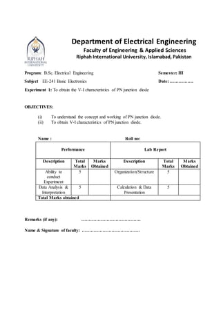
  • 1. Department of Electrical Engineering Faculty of Engineering & Applied Sciences Riphah International University, Islamabad, Pakistan Program: B.Sc. Electrical Engineering Semester: III Subject EE-241 Basic Electronics Date: ……………. Experiment 1: To obtain the V-I characteristics of PN junction diode OBJECTIVES: (i) To understand the concept and working of PN junction diode. (ii) To obtain V-I characteristics of PN junction diode. Name : Roll no: Performance Lab Report Description Total Marks Marks Obtained Description Total Marks Marks Obtained Ability to conduct Experiment 5 Organization/Structure 5 Data Analysis & Interpretation 5 Calculation & Data Presentation 5 Total Marks obtained Remarks (if any): …………………………………. Name & Signature of faculty: …………………………………
  • 2. Introduction: The semiconductor diode is formed by doping P-type impurity in one side and N- type of impurity in another side of the semiconductor crystal forming a p-n junction as shown in the following figure. At the junction initially free charge carriers from both side recombine forming negatively charged ions in P side of junction (an atom in P -side accept electron and becomes negatively charged ion) and positively charged ion on n side(an atom in n- side accepts hole i.e. donates electron and becomes positively charged ion)region. This region deplete of any type of free charge carrier is called as depletion region. Further recombination of free carrier on both sides is prevented because of the depletion voltage generated due to charge carriers kept at distance by depletion (acts as a sort of insulation) layer as shown dotted in the above figure. Working principle: When voltage is not applied across the diode, depletion region forms as shown in the above figure. When the voltage is applied between the two terminals of the diode (anode and cathode) two possibilities arises depending on polarity of DC supply. 1. Forward-Bias Condition: When the +Ve terminal of the battery is connected to P-type material & -Ve terminal to N-type terminal as shown in the circuit diagram, the diode is said to be forward biased. The application of forward bias voltage will force electrons in N-type and holes in P-type material to recombine with the ions near boundary and to flow crossing junction. This reduces width of depletion region. This further will result in increase in majority carriers flow across the junction. If forward bias is further increased in magnitude the depletion region width will continue to decrease resulting in exponential rise in current as in ideal
  • 3. diode characteristic curve. 2. Reverse-biased: If the negative terminal of battery (DC power supply) is connected with P-type terminal of diode and +Ve terminal of battery connected to N type then diode is said to be reverse biased. In this condition the free charge carriers (i.e. electrons in N-type and holes in P-type) will move away from junction widening depletion region width. The minority carriers (i.e. -ve electrons in p-type and +ve holes in n-type) can cross the depletion region resulting in minority carrier current flow called as reverse saturation current (Is). As no of minority carrier is very small so the magnitude of few microamperes. Ideally current in reverse bias is zero. In short current flows through diode in forward bias, and does not flow through diode in reverse bias. Diode can pass current only in one direction. Experiment Procedure:  Connect the power supply, voltmeter, current meter with the diode as shown in the figure for forward bias diode. You can use two multimeter (one to measure current through diode and other to measure voltage across diode)   Increase voltage from the power supply from 0V to 20V in step as shown in the observation table    Measure voltage across diode and current through diode. Note down readings in the observation table.    Reverse DC power supply polarity for reverse bias    Repeat the above procedure for the different values of supply voltage for  reverse bias Draw VI characteristics for forward bias and reverse bias in one graph Circuit diagram (forward bias) Circuit diagram (Reverse bias)
  • 4. Observation table: (Forward bias) Sr. Supply Diode Diode No Voltage Voltage Current (Volts) Vd Id 1 0.2 0.144 0 2 0.4 0.364 0 3 0.6 0.456 0.05 4 0.8 0.516 0.21 5 1.0 0.547 0.43 6 2.0 0.599 1.3 3.0 0.626 2.3 4.0 0.642 3.4 5.0 0.654 4.3 6.0 0.664 5.4 Observation table: (Reverse bias) Sr. Supply Diode Diode No Voltage Voltage Current (Volts) Vd Id 1 0.2 0.12 0 2 0.4 0.36 0 3 0.6 0.54 0 4 0.8 0.72 0 5 1.0 0.89 0 6 2.0 1.93 0 3.0 2.99 0 4.0 3.99 0 5.0 4.99 0 6.0 5.93 0 Draw V-I characteristics of PN junction diode:
  • 5. Questions: [1] List important specifications of the diode Ans: Specifications of Diode  Maximum repetitive reverse voltage = 100 V.  Average rectified forward current = 200 mA.  Maximum direct forward current = 300 mA.  Maximum forward voltage drop = 1.0 V at 10 mA.  Non-repetitive peak forward surge current = 1.0 A (pulse width = 1 s)  Total power dissipation = 500 MW. [2] What is breakdown voltage? What is the breakdown voltage of diode 1N4001 and 1N4007? Ans:. Breakdown Voltage: The breakdown voltage of an insulator is the minimum voltage thatcauses a portion of an insulator to become electrically conductive. For diodes, the breakdownvoltage is the minimum reverse voltage that makes the diode conduct appreciably in reverse.1N4001 Diode will break down at 50 volts or less and 1N4007 diode will breakdown at1000V. [3] List different types of the diode Ans: Types of Diodes Laser diode. Avalanche diode. Light Emitting Diode. Zener diode. Schottky diode. Photodiode. PN junction diode. [5] How to check diode with help of multimeter? Ans: Connect the red probe of the multimeter to the anode and black probe to the cathode. This means the diode is forward-biased. Observe the reading on multimeter's display. If the displayed voltage value is in between 0.6 to 0.7 (for a Silicon Diode), then the diode is healthy and perfect [6] What is the reason for reverse saturation current ? Ans: The reverse saturation current is the part of the reverse current in a semiconductor diode which is caused by the diffusion of minority carriers from the neutral regions to the depletion region. [7] What is the forward voltage drop of silicon diode and germanium diode? Ans: Forward voltage for a diode varies only slightly for changes in forward current and temperature, and is fixed by the chemical composition of the P-N junction. Silicon diodes have a forward voltage of approximately 0.7 volts. Germanium diodes have a forward voltage of approximately 0.3 volts.
  • 6. Observations & Discussion Whena diode isconnectedina ForwardBias condition,anegative voltage isappliedtothe N-type material andapositive voltageisappliedtothe P-type material.Inthe forwardbiased condition, the current varies with the voltage. When a diode is connected in a Reverse Biascondition,apositive voltage isappliedtothe N-type material andanegative voltageis appliedtothe P-type material.Inreversedbiasedconditionthe voltagesremainsame,butthe currentis zeroat any point.This isdue the wide depletionregionthe smallcurrentflowsbut itsalmostzeroand neglected. Conclusion: In today’s lab I learned about the diode, types of Diode its specifications and its characteristics.Ialsolearnedaboutthe workingof the Diode,itsPN Junction,holes,and electrons depletion region. I also learned about the Forward biased and Reverse biased Conditionsof the diode.Ilearnedaboutthe interiorof the diode.