SlideShare ist ein Scribd-Unternehmen logo
1 von 111
Downloaden Sie, um offline zu lesen
Plasma TV
Chassis F82A
Model Code PS43D450A2WXZG
SERVICEMANUAL
Plasma TV
PS43D450A2W
Refer to the service manual in the GSPN (see the rear cover) for more information.
1. Precaution
1. Precaution
To avoid possible damage, electric shocks or exposure to radiation, follow the instructions below with regard to safety,
installation, service and ESD.
1.1. Safety Precautions
1) Make sure all protective devices are properly installed including non-metallic handles and compartment covers when
installing or re-installing the chassis or chassis assemblies.
2) Make sure that no gaps exist between the cabinets for children to insert their fingers in to prevent children from
receiving electric shocks. Gaps mentioned above include ventilation holes of a too great magnitude between the PDP
module and the cabinet mask, and the improper installation of the rear cabinet.
Errors may occur when the resistance is below 1.0MΩ or over 5.2MΩ. In these cases, make sure that the device is
repaired before sending it back to the customer.
3) Check for Electricity Leakage (AC Leakage Test)
WARNING
Do not use an insulated transformer for checking the leakage. Use only those current leakage testers or mirroring
systems that comply with ANSIC 101.1 and the Underwriter Laboratory’s specifications (UL1410, 59.7).
DEVICE
UNDER
TEST
LEAKAGE
CURREN T
TESTER
TES T ALL
EXPOSED ME TAL
SUR FACES
2-WIRE CORD
ALSO TES T WITH
PLUG REVERSED
(USING AC
ADAPTER PLUG
AS REQU IRED)
EARTH
GROUND
( R E A D I N G
SHOULD NOT BE
ABOVE 0.5mA)
Figure 1.1 AC Leakage Test
4) A high voltage is maintained within the specified limits using safety parts, calibration and tolerances. When voltage
exceeds the specified limits, check each special part.
5) Warning for Engineering Changes:
Never make any changes or additions to the circuit design or the internal part for this product.
Ex: Do not add any audio or video accessory connectors. This might cause physical damage.
Furthermore, any changes or additions to the original design/engineering will invalidate the warranty.
6) Warning - Hot Chassis:
Some TV chassis are directly connected to one end of the AC power cord for electrical reasons. Without insulated
transformers, the product can only be repaired safely when the chassis is connected to the earthed end of the AC
power source.
To make sure the AC power cord is properly connected, follow the instructions below. Use the voltmeter to measure the
voltage between the chassis and the earthed ground. If the measurement is over 1.0V, unplug the AC power cord and
change the polarity before reinserting it. Measure the voltage between the chassis and the ground again.
Copyright© 1995-2011 SAMSUNG. All rights reserved. 1-1
1. Precaution
7) Some TV chassis are shipped with an additional secondary grounding system. The secondary system is adjacent to
the AC power line. These two grounding systems are separated in the circuit using an unbreakable/unchangeable
insulation material.
8) When any parts, material or wiring appear overheated or damaged, replace them with new regular ones immediately.
When any damage or overheating is detected, correct this immediately and make a regular check of possible errors.
9) Check for the original shape of the lead, especially that of the antenna wiring, any sharp edges, the AC power and the
high voltage power. Carefully check if the wiring is too tight, incorrectly placed or loose. Never change the space
between the part and the printed circuit board. Check the AC power cord for possible damages. Keep the part or the
lead away from any heat-emitting materials.
10) Safety Indication:
Some electrical circuits or device related materials require special attention to their safety features, which cannot be
viewed by the naked eye. If an original part is replaced with another irregular one, the safety or protective features will
be lost even if the new one has a higher voltage or more watts.
Critical safety parts should be bracketed with ( , ). Use only regular parts for replacements (in particular, flame
resistance and dielectric strength specifications). Irregular parts or materials may cause electric shock or fire.
1-2 Copyright© 1995-2011 SAMSUNG. All rights reserved.
1. Precaution
1.2. Servicing Precautions
WARNING
1) First carefully read the “Safety Instruction” in this service manual.
When there is a conflict between the service and the safety instructions, follow the safety instruction at all times.
2) Any electrolytic capacitor with the wrong polarity will explode.
1) The service instructions are printed on the cabinet, and should be followed by any service personnel.
2) Make sure to unplug the AC power cord from the power source before starting any repairs.
a) Remove or re-install parts or assemblies.
b) Disconnect the electric plug or connector, if any.
c) Connect the test part in parallel with the electrolytic capacitor.
3) Some parts are placed at a higher position than the printed board. Insulated tubes or tapes are used for this purpose.
The internal wiring is clamped using buckles to avoid contact with heat emitting parts. These parts are installed back
to their original position.
4) After the repair, make sure to check if the screws, parts or cables are properly installed. Make sure no damage is caused
to the repaired part and its surroundings.
5) Check for insulation between the blade of the AC plug and that of any conductive materials (i.e. the metal panel,
input terminal, earphone jack, etc).
6) Insulation Check Process:
Unplug the power cord from the AC source and turn the switch on. Connect the insulating resistance meter (500V) to
the AC plug blade. The insulating resistance between the blade of the AC plug and that of the conductive material
should be more than 1MΩ.
7) Any B+ interlock should not be damaged.
If the metal heat sink is not properly installed, no connection to the AC power should be made.
8) Make sure the grounding lead of the tester is connected to the chassis ground before connecting to the positive lead.
The ground lead of the tester should be removed last.
9) Beware of risks of any current leakage coming into contact with the high-capacity capacitor.
10) The sharp edges of the metal material may cause physical damage, so protect yourself by wearing gloves during the
repair.
11) Due to the nature of plasma display panels, partial after-images may appear if a still picture is displayed on the screen
for a long period of time.
This is caused by brightness deterioration due to the storage effect of the panel, and to prevent this from happening, we
recommend that the brightness and contrast are reduced. (e.g.) Contrast: 25, Brightness: 50
Copyright© 1995-2011 SAMSUNG. All rights reserved. 1-3
1. Precaution
1.3. Static Electricity Precautions
1) Some semi-conductive (“solid state”) devices are vulnerable to static electricity. These devices are known as ESD.
ESD includes the integrated circuit and the field effect transistor. To avoid any materials damage from electrostatic
shock, follow the instructions described below.
2) Remove any static electricity from your body by connecting the earth ground before handling any semi-conductive parts
or assemblies. Alternatively, wear a dischargeable wrist-belt.
(Make sure to remove any static electricity before connecting the power source - this is a safety instruction for
avoiding electric shock)
3) Remove the ESD assembly and place it on a conductive surface such as aluminum foil to prevent accumulating static
electricity.
4) Do not use any Freon-based chemicals. Such chemicals will generate static electricity that causes damage to the ESD.
5) Use only grounded-tip irons for soldering purposes.
6) Use only anti-static solder removal devices.
Most solder removal devices do not support an anti-static feature. A solder removal device without an anti-static feature
can store enough static electricity to cause damage to the ESD.
7) Do not remove the ESD from the protective box until the replacement is ready. Most ESD replacements are covered with
lead, which will cause a short to the entire unit due to the conductive foam, aluminum foil or other conductive materials.
8) Remove the protective material from the ESD replacement lead immediately after connecting it to the chassis or
circuit assembly.
9) Take extreme caution in handling any uncovered ESD replacements. Actions such as brushing clothes or lifting your leg
from the carpet floor can generate enough static electricity to damage the ESD.
CAUTION
These servicing instructions are for use by qualified service personnel only.
To reduce the risk of electric shock do not perform any servicing other than that contained in the operating instructions
unless you are qualified to do so.
1-4 Copyright© 1995-2011 SAMSUNG. All rights reserved.
1. Precaution
1.4. Installation Precautions
1) For safety reasons a minimum of two people are required to carry this product.
2) Keep the power cord away from any heat emitting devices, as a melted covering may cause fire or electric shock.
3) Do not place the product in areas with poor ventilation such as a bookshelf or closet. The increased internal temperature
may cause fire.
4) Bend the external antenna cable when connecting it to the product. This is a measure to protect it from being exposed to
moisture. Otherwise, it may cause a fire or electric shock.
5) Make sure to turn the power off and unplug the power cord from the outlet before repositioning the product. Also
check the antenna cable or the external connectors if they are fully unplugged. Damage to the cord may cause fire
or electric shock.
6) Keep the antenna far away from any high-voltage cables and install it firmly. Contact with the high-voltage cable or the
antenna falling over may cause fire or electric shock.
7) When connecting the RF antenna, check for a DTV receiving system and install a separate DTV reception antenna for
areas with no DTV signal.
8) When installing the product, leave enough space (4”) between the product and the wall for ventilation purposes. A
rise in temperature within the product may cause fire.
9) When moving a PDP with removable speakers, detach the speakers first before moving the main body. Moving the PDP
main body without separating the speakers may cause the speakers to detach, possibly causing damage or injury.
Copyright© 1995-2011 SAMSUNG. All rights reserved. 1-5
2. Product Specification
2.1. Product Feature
■ Features
Block Specification Major IC Remark
RF Digital/Analog (DTV Built In)
PDP Module SDI DH MODULE
43” HD
51” HD
New Module
Power
SAMSUNG ELECTRO MECHANICS
SMPS DOYANG SMPS
Video
NTSC 3.58 ATSC
HDMI
Component, PC
MSD 2248
Sound SRS TruSuround HD, Dolby Digital TAS 5715 Optical Output
Cabinet C490 Design
Copyright© 1995-2011 SAMSUNG. All rights reserved. 2-1
2. Product Specification
■ Specification
Model P*43D4*0 P*51D4*0
Dimensions (W x H x D)
39.8 x 27.5 x 12 inches - with stand
39.8 x 24.5 x 2.2 inches - without stand
46.7 x 30.8 x 12 inches - with stand
46.7 x 27.8 x 2.2 inches - without stand
Weight
41.8 lbs - with stand
35.2 lbs - without stand
56.2 lbs - with stand
49.6 lbs - without stand
Panel Resolution 1024 x 768 1360 x 768
PC Resolution 1920 (H) x 1080 (V)
Screen Size 43 Inches (16:9) 51 Inches (16:9)
Power Consumption 43 HD: 200W ±10% and Less 51 HD : 280W ±10% and Less
Antenna Input
ANT - AIR / CABLE IN
75Ω unbalanced
W/W
AV
COMPONENT1 - 480i / 480p / 720p / 1080i / 1080p
COMPONENT2 - 480i / 480p / 720p / 1080i / 1080p
PC
HDMI1 – 480p / 720p / 1080i / 1080p
HDMI2 (DVI Compatible) – 480p / 720p / 1080i / 1080p
HDMI3 (SIDE AV) – 480p / 720p / 1080i / 1080p
480i can be displayed on HDMI, however it is not contained in EDID data.
Video Input
EU
AV
COMPONENT1 - 480i / 480p / 720p / 1080i / 1080p
SCART - 21P, Sn, BLK
PC
HDMI1 – 480p / 720p / 1080i / 1080p
HDMI2 (DVI Compatible) – 480p / 720p / 1080i / 1080p
HDMI3 (SIDE AV) – 480p / 720p / 1080i / 1080p
480i can be displayed on HDMI, however it is not contained in EDID data.
Audio Input
AV
COMPONENT 1 - 480i / 480p / 720p / 1080i / 1080p
COMPONENT 2 - 480i / 480p / 720p / 1080i / 1080p
PC
DVI
Audio Output AUDIO (L/R)
Speaker Output 10W + 10W (40dB + 40dB)
New Features 3D Built-In
2-2 Copyright© 1995-2011 SAMSUNG. All rights reserved.
2. Product Specification
2.2. Specifications Analysis
Model P*43D4*0 P*51D4*0 P*42C450*
Design
Display Type PDP TV PDP TV PDP TV
Built-In Tuner O O O
Resolution 1024 x 768 1365 x 768 1024 x 768
PDP Module DH DH U2P
Screen Size 43 inches 51 inches 42 inches
Basic
Picture ratio 16 : 9 16 : 9 16 : 9
Brightness 1,500 Cd/m2 1,500 Cd/m2 1,500 Cd/m2
Contrast Ratio 10,000 : 1 10,000 : 1 30,000 : 1Picture
Picture Enhacer DNIe (SEMS20) DNIe (SEMS20) DNIe
Equalizer 5 Band 5 Band 5 Band
Auto Volume Control O O O
Surround Sound SRS Theater Sound SRS Theater Sound SRS TruSurround HD
Audio
Speaker Output 10W + 10W 10W + 10W 10W + 10W
PIP O O O
Double Screen X X X
Caption O O O
Still Image X X X
EPG O O O
My color Control X X X
Energy Saving O O O
Screen Burn Protection O O O
Features
Anynet X X O
Antenna 1 (Cable/Air) 1 (Cable/Air) 1 (Cable/Air)
AV Input 1 Input 1 Input 1 Input
S-Video X X X
W/W 2 Input 2 Input 2 Input
Component
EU 1 Input 1 Input 1 Input
PC (D-SUB) 1 Input 1 Input 1 Input
DVI X X X
HDMI
D490 – 3 Input
D450 – 2 Input
D490 – 3 Input
D450 – 2 Input
4 Input
USB 1 1 1
Sub Woofer X X X
Connections
Optical 1 1 1
Etc. Speaker/Stand Built-in Speaker Built-in Speaker Built-in Speaker
Copyright© 1995-2011 SAMSUNG. All rights reserved. 2-3
2. Product Specification
TIP
O : Supported, X : Not Supported
NOTE
For the power supply and power consumption, refer to the label attached to the product.
2-4 Copyright© 1995-2011 SAMSUNG. All rights reserved.
2. Product Specification
2.3. Accessories
2.3.1. Supplied Accessories
Accessories Item Item code Remark
A B C D
Remote Control AA59-00484A
Batteries 4301-000103
Power Cord 3903-000456
Owner`s
Instructions
BN68-03491C
Cloth-Clean BN63-01798B
Ferrite Core for
Power Cord
3301-002049
Samsung Service
Center
Copyright© 1995-2011 SAMSUNG. All rights reserved. 2-5
2. Product Specification
2.3.2. Sold Separately
Accessories Item Item code Remark
RS232 Cable -
HDMI -
HDMI-DVI -
Component -
Composite (AV) -
Coaxial (RF) -
VGA -
Samsung Service Center
2-6 Copyright© 1995-2011 SAMSUNG. All rights reserved.
3. Disassembly & Reassembly
3.1. Overall Disassembly & Reassembly
CAUTION
• Be sure to separate the power cord before
disassembling the unit.
• Discharge the capacitors first when separating PCB’s
with high capacity capacitors such as SMPS, X
Main Board, Y Main Board, etc. (A spark may be
generated by the electric charge, and there is danger
of electronic shock.)
• Check that the cables are properly connected
referring to the circuit diagram when disassembling
or assembling the unit taking care not to damage the
cables
• Take care not to scratch the Glass Filter in the front.
• Assemble the boards in the reverse order of the
disassembly.
• The plasma must be layed down on a flat padded
surface for disassembly and reassembly.
1. Place monitor face down on cushioned table. Remove
screws from the Stand. Remove stand.
* Rear view of 43"
<43" PDP>
<43" PDP>
6001–002621 : M4 * L8
Copyright© 1995-2011 SAMSUNG. All rights reserved. 3-1
3. Disassembly & Reassembly
* Rear view of 51"
<51" PDP>
<51" PDP>
6001–002621 : M4 * L8
2. Remove the screws of rear-cover.
* Rear view of 43"
<43" PDP>
6003–001782 : M4 * L12
6003–000337 : M4 * L10
* Rear view of 51"
<51" PDP>
6003–001782 : M4 * L12
6003–000337 : M4 * L10
3-2 Copyright© 1995-2011 SAMSUNG. All rights reserved.
3. Disassembly & Reassembly
3. Lift up and remove the rear-cover.
* Rear view of 43"
<43" PDP>
* Rear view of 51"
<51" PDP>
4. Remove the screws of main board.
CAUTION
Disconnect all connectors prior to removing boards.
6001–002606 : M3 * L10
5. Remove the screws of SMPS. Remove the SMPS.
CAUTION
Align board under tab when re-installing.
6001–002606 : M3 * L10
6003–001439 : M4 * L8
6. Remove the speakers. (R/L)
Copyright© 1995-2011 SAMSUNG. All rights reserved. 3-3
3. Disassembly & Reassembly
7. Remove the Cover Bottom.
8. Remove the screw of Bluetooth Module.
NOTE
PD49X Series Only.
6001–002606 : M3 * L10
9. Remove the screws of Bracket Stand Link. Lift up the
Stand Bracket Stand Link.
6003–001782 : M4 * L12
6003–000337 : M4 * L10
10. Remove the screws of the front-cover.
* Rear view of 43"
<43" PDP>
6003–001782 : M4 * L12
* Rear view of 51"
<51" PDP>
6003–001782 : M4 * L12
3-4 Copyright© 1995-2011 SAMSUNG. All rights reserved.
3. Disassembly & Reassembly
3.2. Method for Disassembly of Function Assy
1. Put up the upper Locking, Use screwdriver.
2. Put up the lower Locking, Use screwdriver.
3. Remove Locking.
4. Detach the Function PBA.
CAUTION
Disconnect all connectors prior to removing boards.
Copyright© 1995-2011 SAMSUNG. All rights reserved. 3-5
4. Troubleshooting
4. Troubleshooting
4.1. Checkpoints by Error Mode
4.1.1. First Checklist for Troubleshooting
1) Check the various cable connections first.
• Check to see if there is a burnt or damaged cable.
• Check to see if there is a disconnected or loose cable connection.
• Check to see if the cables are connected according to the connection diagram.
2) Check the power input to the Main Board.
3) How to distinguish if the problem is caused by Main board or Logic Board.
• No Video : If the problem is No Video but Logic Board is on and Indication LED is blinking repeatedly and
faster than normal booting, replace the T-Con board.
• Distorted Picture : Check the inner patterns.
Inner pattern Picture Problem
OK NG Main board
NG NG Main or LVDS cable or Logic Board or Panel.
• How to check inner pattern?
a. Factory mode (mute → 1 → 8 → 2 → Power on when TV is in ‘stand - by mode’ )
b. Move to SVC menu.
c. Move to Test Pattern.
d. Check inner patterns.
Copyright© 1995-2011 SAMSUNG. All rights reserved. 4-1
4. Troubleshooting
4.1.2. Checkpoints by Error Mode
■ No Power
Symptom
• The LEDs on the front panel do not work when connecting the power cord.
• The SMPS relay does not work when connecting the power cord.
• The unit appears to be dead.
Major Checklist
The SMPS relay or the LEDs on the front panel does not work when connecting the power cord if
the cables are improperly connected or the Main Board or SMPS is not functioning. In this case,
check the following:
• Check the internal cable connection status inside the unit.
• Check the fuses of each part.
• Check the output voltages of the SMPS.
• Replace the Main Board.
Diagnostics
Fuse
CN801
CN201
<43" PDP>
Fuse
CN801
CN201
<51" PDP>
4-2 Copyright© 1995-2011 SAMSUNG. All rights reserved.
4. Troubleshooting
Yes
Yes
Yes
Yes
Power indicator LED is on? Check AC power connection.
Replace the Main Board.
Connect the cable between
CN801 and CN201 connector.
Are the SMPS CN801 and Main CN201
connected?
Replace Fuse. (F801S)
Is the Fuse(F801S) of the SMPS Power
Input Part Open?
Replace the SMPS.
SMPS CN801
PIN2 : STB5V
PIN1_ PS ON : Check to see if it is 0V?
No
No
No
No
CAUTION
Make sure to disconnect the power before working on the SMPS board.
Copyright© 1995-2011 SAMSUNG. All rights reserved. 4-3
4. Troubleshooting
■ No Video
Symptom • Audio is normal but no picture is displayed on the screen.
Major Checklist
• The output voltage of the Main SMPS.
• This may happen when the LVDS cable connecting the Main Board and the Panel is
disconnected.
Diagnostics
LVDS cable
<43" PDP>
LVDS cable
<51" PDP>
4-4 Copyright© 1995-2011 SAMSUNG. All rights reserved.
4. Troubleshooting
Check the LED
Operation.
Yes
Yes
Yes
Replace the Main Board.
Check / Replace the LVDS Cable.
Check the LVDS connector.
Is it connected correctly?
Replace the SMPS.
Check All output voltages on SMPS.
Are all voltages normal?
Replace the Logic Board.
Check the LED operation of Logic Board
whitch is normally operating?
(Normal : Blink once a second)
No
No
No
CAUTION
Make sure to disconnect the power before working on the SMPS board.
Copyright© 1995-2011 SAMSUNG. All rights reserved. 4-5
4. Troubleshooting
■ No Sound
Symptom • Video is normal but there is no sound.
Major Checklist
• When the speaker connectors are disconnected or damaged.
• When the sound processing part of the Main Board is not functioning.
• Speaker defect.
• SMPS not supplying voltage to the main board.
Diagnostics <43" PDP>
Speaker
Speaker cable
CN801
<51" PDP>
4-6 Copyright© 1995-2011 SAMSUNG. All rights reserved.
4. Troubleshooting
Yes
Yes
Yes
Replace the Speaker.
Replace the SMPS.
Is the output voltage of SMPS normal?
(CN801 7pin : 15V)
Replace the Main board.
(1)
Is the speaker output terminal of
the Main board normal?
Connect the cable properly or
replace the cable, if necessary.
Is the cable connection between
Main board and the speaker
properly connected?
No
No
No
Sound OutputShape
(1)
CAUTION
Make sure to disconnect the power before working on the IP board.
Copyright© 1995-2011 SAMSUNG. All rights reserved. 4-7
4. Troubleshooting
4.1.3. Faults and Corrective Actions
Symptom Related Image Causes and Countermeasures
A blank vertical cell (block)
appears on the screen.
• Address buffer defect
• Replace the corresponding upper/lower buffers.
(E, F or G)
• COF defect (burnt)
• Replace the module.
A green screen appears when
the TV is turned on.
• The Scale is not reseting.
• Replace the Main board.
The OSD box appears but
there is no text.
• Incorrect program version.
• Check the version of each program.
• Replace the Main board.
A blank upper (or lower)
block appears on the screen.
• Upper/Lower Y Buffer defect
• Replace the corresponding upper/ lower buffers.
Either the main or sub picture
does not appear.
• Replace the Main board.
A vertical green line appears
on the screen.
• The SMPS voltage is incorrect.
• Adjust the SMPS voltage according to the voltage
printed on the module label.
4-8 Copyright© 1995-2011 SAMSUNG. All rights reserved.
4. Troubleshooting
Symptom Related Image Causes and Countermeasures
Dim screen (blurred in red)
• X-Main board defect
• Replace the X-Main board.
A blank screen appears. • Replace the Y-Main board.
Copyright© 1995-2011 SAMSUNG. All rights reserved. 4-9
4. Troubleshooting
4.1.4. Operating Logic LED
■ Normal
• LED ON/OFF for 0.5s
OFF
ON
Power ON Logic ON Sequence (POS) Normal Toggling
(every 32 Vsync)
-. NT : 534 ms
-. PAL : 640 ms
■ Abnormal
• LED ON/OFF three times for 8.1s
540
ms
8.06
sec
Exception
540
ms
540
ms
540
ms
540
ms
27Mhz
2.44
sec
163
ms
PLL ON
163
ms
163
ms
163
ms
163
ms
··ªª µµ ªª ¦¦ ¹¹ee...
■ DRV_RESET
• LED ON for 5s and LED OFF for 2s
5
sec
··ªª µµ ªª ¦¦ ¹¹ee...
DRV_RESET
2
sec
4-10 Copyright© 1995-2011 SAMSUNG. All rights reserved.
4. Troubleshooting
4.1.5. Adjust Function Key Sensitivity
1) Select 'Factory'
2) Select 'Control'
Copyright© 1995-2011 SAMSUNG. All rights reserved. 4-11
4. Troubleshooting
3) Select 'Sub Option'
4) Select 'Key Sensitivity'
4-12 Copyright© 1995-2011 SAMSUNG. All rights reserved.
4. Troubleshooting
5) Default value (PD490=56, PD550=32)
6) Adjust The Value of Key Sensitivity
No use 'Key Sens itivity' Very Sensitive Insensitive
Copyright© 1995-2011 SAMSUNG. All rights reserved. 4-13
4. Troubleshooting
4.1.6. Function Assy Pin Map
■ US Main Board
CN1201
Pinmap
1. IR
2. GND
3. A3.3V
4. SCL
5. SDA
6. FUNC_INTR
7. LED_STB
■ EU Main Board
CN1201
Pinmap
1. IR
2. GND
3. A3.3V
4. SCL
5. SDA
6. FUNC_INTR
7. LED_STB
4-14 Copyright© 1995-2011 SAMSUNG. All rights reserved.
4. Troubleshooting
4.1.7. Adjust SMPS Voltage when change SMPS
VS_TP
VS_VR
VA_TP
VA_VR
VS_TP
VS_VR
VA_TP
VA_VR
TIP
• T.P : Test Point
• V.R : Variable Resistor
Copyright© 1995-2011 SAMSUNG. All rights reserved. 4-15
4. Troubleshooting
4.2. Factory Mode Adjustments
4.2.1. Entering Factory Mode
To enter ‘Service Mode’ Press the remote-control keys in this sequence.
• If you do not have Factory remote-control.
ŸŸ ¾¾ ÆÆ ´´ ÁÁoožž •• •• oo ŸŸ ¾¾ ÆÆ ´´ ÁÁoožž ˜˜ •• žž œœ ””  ¤¤ oo”” ¤¤ œœ ¤¤ ££ ”” oo
ŸŸ ¾¾ ÆÆ ´´ ÁÁoožž •• •• oo ŸŸ ¾¾ ÆÆ ´´ ÁÁoožž œœ ¤¤ ££ ”” oo¦¦ ~~ ¦¦ €€ ‡‡ 
• If you have Factory remote-control.
INFO Factory
• If you don’t have Factory remote control, can’t control some menu.
Option
Control
SVC
Expert
ADC / WB
Advanced
T-MST4AUSC-0408.0
T-MST4AUSS-0019
E-Manual : X6ATSCA-0003
EDID SUCCESS
HDCP SUCCESS
CALIB : AV O COMP O PC O HMDI O
Option : 2701, 1374
SDAL-0.58.1.0
RFS : "Mstar-X5 0039"
KERNEL MODULE VERSION: "00035_90"
2010-12-08
Type : 51DFHcD
Model : PN51D550
MAC SUCCESS
LOCD X
Factory Data Ver : 68
EERC Version : 501
DTP-AP-COMP-582
DTP-BP-HAL-0083
DTP-BP-0582
Date of purchase : mm/dd/yyyy
4-16 Copyright© 1995-2011 SAMSUNG. All rights reserved.
4. Troubleshooting
4.2.2. Factory Data
■ Option
Item Data Remark
Factory Reset -
Type 43DHHcD
Local Set xx
Model PD490
Tuner xx
Ch table NONE
Front Color T-R-BLK
■ Control
Menu Item Data Remark
EDID EDID ON/OFF ON
EDID WRITE ALL Success
EDID WRITE PC Success
EDID WRITE HDMI ...
EDID WRITE HDMI1 Success
EDID WRITE HDMI2 Success
EDID WRITE HDMI3 Success
EDID WRITE HDMI4 Success
HDMI EDID Ver HDMI 1.2
HDMI EDID Port NONE
EDID WRITE DVI ...
Sub Option RF Mute Time 600ms
RS-232 Jack Debug
Watchdog OFF
WD COUNT 255
Dimm Type
LVDS FORMAT PDP
Language_Arabic xx
TOOLS Support 32
LNA Support 0
DB On with
5MB
MOVIE chapterinmed
DLNA ON
MediaPlay
Play List OFF
NETWORK Support Ext-Wifi
Info Link Server Type development
Copyright© 1995-2011 SAMSUNG. All rights reserved. 4-17
4. Troubleshooting
Menu Item Data Remark
Info Link Country None
TTX List
TTX Group
24Px4 Support OFF
Power Indicator Support OFF
BD Wise Support OFF
Data Service Support OFF
OTA Duration Test OFF
Alternate Del OFF
OTN Server Type operating
OTN Test Server OFF
OTN Support ON
OTN Reset
OTN Duration OFF
OTN Fail Test OFF
IIC BUS STOP OFF
Visual Test Disable
Emergency Log Copy
Checksum 0x0000
Select Log Type IR KEY
Log View
View Log
Delete Log
ColorSpace Support RGB Type
Gemstar On/Off OFF
WSS Support OFF
PVR Support OFF
CI Support OFF
Eepron Reset
LVDS Spread ON
Period 40K
Amplitude 1.5
Spread Spectrum
DDR Spread 1.0% Spread
A CTRL_OFFSET_0_3 0x0
A CTRL_OFFSET_D 0x0
B CTRL_OFFSET_0_3 0x0
DDR Margin
B CTRL_OFFSET_D 0x0
H.264 Margin 8
MPEG Margin 1000
Tuner Margin 10
4-18 Copyright© 1995-2011 SAMSUNG. All rights reserved.
4. Troubleshooting
Menu Item Data Remark
Y0 Ref 165
Y1 Ref 148
Y2 Ref 119
Y3 Ref 101
Y4 Ref 76
Y5 Ref 60
Y6 Ref 31
Y7 Ref 0
Cb0 Ref 128
Cb1 Ref 64
Cb2 Ref 148
Cb3 Ref 85
Cb4 Ref 171
Cb5 Ref 108
Cb6 Ref 194
Cb7 Ref 0
Cr0 Ref 128
Cr1 Ref 137
Cr2 Ref 64
Cr3 Ref 74
Cr4 Ref 181
Cr5 Ref 192
Cr6 Ref 118
SST
Cr7 Ref 0
Y0 TH 20
Y1 TH 20
Y2 TH 20
Y3 TH 20
Y4 TH 20
Y5 TH 20
Y6 TH 20
Y7 TH 20
Cb0 TH 20
Cb1 TH 20
Cb2 TH 20
Cb3 TH 20
Cb4 TH 20
Cb5 TH 20
Cb6 TH 20
Cb7 TH 20
SST_TH
Copyright© 1995-2011 SAMSUNG. All rights reserved. 4-19
4. Troubleshooting
Menu Item Data Remark
Cr0 TH 20
Cr1 TH 20
Cr2 TH 20
Cr3 TH 20
Cr4 TH 20
Cr5 TH 20
Cr6 TH 20
Cr7 TH 20
2nd mips ON
2nd mips count 0
Region xxx
PnP Language xxx
PC Auto Ident Enable
OTP Lock ...
Auto Power MEMORY
KEY SENSITIVITY 56 1(Very Sensitive)~255(Insensitive)
FANET OFF
OTA Support OFF
WIFI REGION V
FKP Down
PDP Option LOGIC CONNECT OFF
PIXEL SHIFT TEST OFF
PANEL VERSION DF
PANEL INCH 51FHD
PANEL TYPE 53
PANEL TEMPERATURE 40
LOGIC ID A712
LOGIC SW VERSION 2010-11-20
LOGIC SW CHECKSUM 0xFC31
MRT 44
SAPC TIMER ON
APC SPEED SLOW
Real 100 Hz Support OFF
XGA Resolution OFF
PLG_SHOP 128
Hotel Option HOTEL MODE ON
POWER ON CHANNEL
EN
User
Defined
POWER ON CHANNEL 3
CHANNEL TYPE CATV
4-20 Copyright© 1995-2011 SAMSUNG. All rights reserved.
4. Troubleshooting
Menu Item Data Remark
POWER ON VOLUME
EN
User
Defined
POWER ON VOLUME 10
MIN VOLUME 0
MAX VOLUME 100
PANEL BUTTON LOCK Unlock
POWER ON SOURCE TV
Picture Menu Lock OFF
Music Mode AV OFF
Music Mode PC OFF
Music Mode Comp OFF
Music Mode Backlight OFF
Menu Display ON
Power On Option Last Option
Auto Source OFF
Energy Saving OFF
Clone TV to USB
Clone USB to TV
Setting Auto initialize OFF
SIRCH Update Time 2:00 AM
MONITOR OUT CVBS ON
Shop Option Shop Mode OFF
Exhibition Mode OFF
Asia Option TTX OFF
China HD OFF
NT Conversion OFF
Sepco 120Hz OFF
Unbalance OFF
FMTransmitter Support OFF
FMTransmitter Carrier OFF
AF Level adjust 3
TX power Level 0
Mono Last Memory OFF
H Shaking OFF
SOUND High Devi OFF
Carrier Mute ON
Volume Curve Type1
Speaker Delay Normal 50
Pilot Level High Thld 0x28h
Pilot Level Low Thld 0x10h
FM Prescale 0
Copyright© 1995-2011 SAMSUNG. All rights reserved. 4-21
4. Troubleshooting
Menu Item Data Remark
AM Prescale 0
NICAM Prescale 0
Amp Volume 0xc7h
Amp Scale 0x82h
Woofer Type 1
Woofer Scale 0x7fh
Woofer Check Sum
Speaker EQ ON
Amp Model 0
Speaker cut-off Freq NTP7411
SPDIF PCM Gain -9 dB
FM M Prescale 48
BTSC Mono Prescale 25
BTSC stereo Prescale 47
SAP Prescale 43
A2 Ident High Thld 31
A2 Ident Low Thld 2
Carrier2 Amp High Thld 4
Carrier2 Amp Low Thld 3
Carrier2 SNR High THR 16
Carrier2 SNR Low THR 80
Audio-IP Test Ready
TruBass-Checksum 0x200190E2
PWM Mode BD
Config Option Num of ATV 1
Num of DTV 1
Num of AV 1
Num of SVIDEO 0
Num of COMP 2
Num of HDMI 4
Num of PC 1
Num of SCART 0
Num of DVI 0
Num of OPTICAL Link 0
Num of MEDIA 1
Num of PANEL KEY 6
Num of USB Port 2
Num of HeadPhone 0
4-22 Copyright© 1995-2011 SAMSUNG. All rights reserved.
4. Troubleshooting
Menu Item Data Remark
Num of RVU 0
MFT Offset 62.5
Select LCD/PDP PDP
HDMI/DVI SEL 1
Indicator Led OFF
Wall Mount OFF
HV Flip OFF
Num Of Display 2
DVI/HDMI SOUND Auto
HDMI HOT PLUG Disable
HOTPLUG SWITCHING Boot
HOT PLUG DURATION 1200ms
CLK TERM DURATION 1200ms
HDMI FLT CNT SIG 100ms
HDMI FLT CNT LOS 100ms
UNSTABLE BAN CNT 3500ms
HDMI Err Cnt 1
HDMI ROBIN ON
HDMI Callback OFF
HDMI CTS Thld 8
HDMI CTS Cnt1 1
TMDS_EQ2_Boost 1
TMDS_EQ2_Gain 0
TMDS_PLL_Loop 3
TMDS_CPREG_BLEED 1
HDMI EQ Auto
HDMI EDID wRITE Type Separate
HDMI Switch NONE
DVI SET TIME 300ms
Type Of PANEL KEY PDPVertical
EcoSensor Support ON
LEDMotionPlus Support OFF
Natural Mode Support OFF
All Share Support ON
Copyright© 1995-2011 SAMSUNG. All rights reserved. 4-23
4. Troubleshooting
Menu Item Data Remark
Relax Mode Support OFF
DVI-I Support
Melfas Function Support
Light Level Support
H Write
HDMI Sync DE
HeadPhone Port A Out2
SCC SCC Mode Dynamic
SCC ON/OFF OFF
Hx 272
Hy 278
Lx 272
SCC Input Data
Ly 278
sSCC Hx 550
sSCC Hy 566
sSCC Lx 598
sSCC Const
sSCC Ly 550
pSCC Hx 550
pSCC Hy 566
pSCC Lx 598
pSCC Const
pSCC Ly 550
SCC Source Data PBA
SWAP PBA
4-24 Copyright© 1995-2011 SAMSUNG. All rights reserved.
4. Troubleshooting
■ SVC
Menu Item Data Remark
Test Pattern Pattern Sel ...
LOGIC Pattern Sel 0
LOGIC Level Sel 255
Panel Auto Setting Failure
PANEL DISPLAY
TIME
2Hr
LOGIC USB D/L off
Tuner Status
T-CON USB
Download
Failure
MICOM
UPGRADE
Off
BT ADDRESS e4e0c53197db
BT UPGRADE
SVC Reset
■ Expert
Menu Item Data Remark
N/D ADJ OFF
Source ...
■ ADC/WB
Menu Item Data Remark
ADC AV Calibration
Comp Calibraion
PC Calibration
HDMI Calibration
ADC Target 1st_AV_Low 64
1st_AV_High 880
1st_AV_Delta 2
1st_COMP_Y_Low 64
1st_COMP_Cb_Low 512
1st_COMP_Cr_Low 512
1st_COMP_Y_High 940
1st_COMP_Cb_High 512
1st_COMP_Cr_High 512
1st_COMP_Delta 2
1st_PC_Low 4
1st_PC_High 1004
Copyright© 1995-2011 SAMSUNG. All rights reserved. 4-25
4. Troubleshooting
Menu Item Data Remark
1st_PC_Delta 2
2nd_ACH_Low 4
2nd_ACH_High 940
2nd_PC_Low 4
2nd_PC_High 940
2nd_Delta 2
ADC Result 1st_Y_GH 258
1st_Y_GL 128
1st_Cb_BH
1st_Cb_BL
1st_Cr_RH
1st_Cr_RL
2nd_R_L 133
2nd_G_L 133
2nd_B_L 133
2nd_R_H 70
2nd_G_H 70
2nd_B_H 70
White Balance Sub Brightness 128
R-Offset 128
G-Offset 128
B-Offset 128
Sub Contrast 128
R-Gain 128
G-Gain 128
B-Gain 128
Movie R-Offset
Movie B-Offset
Movie R-Gain
Movie B-Gain
■ Advanced
• Picture_2D
Menu Item Data Remark
Sub Setting Gamma 0.95
Natural Gamma 0
Pwm Max 100
PWM Min 0
Pwm Mid 0
Contrast Dimming OFF
4-26 Copyright© 1995-2011 SAMSUNG. All rights reserved.
4. Troubleshooting
Menu Item Data Remark
7.5 IRE NTSC OFF
7.5 IRE Offset
Comp Phase 110
Led Peak OnOff OFF
Dither Bypass OFF
D Motion Light On
Dynamic Contrast On
EPA Standard Standard Contrast 100
Standard Brightness 45
Standard Sharpness 50
Standard Color 50
Standard Tint 0
Standard Backlight 10
WB Movie W/B Movie On/Off OFF
Model ...
Color Tone ...
Msub Brightness ...
Msub Contrast ...
N_Rgain ...
N_Bgain ...
N_Roffset ...
N_boffset ...
W2_Rgain ...
W2_Bgain ...
W2_Roffset ...
W2_Boffset ...
Movie Contrast ...
Movie Bright ...
Movie Color ...
Movie Sharpness ...
Movie Tint ...
Movie Backlight ...
Movie Gamma ...
M_Sub_Gamma ...
HDMI Black Level ...
WCE WRHue 64
WRSat 16
WYHue 64
WYSat 16
WGHue 64
Copyright© 1995-2011 SAMSUNG. All rights reserved. 4-27
4. Troubleshooting
Menu Item Data Remark
WGSat 16
WCHue 64
WCSat 16
WBHue 64
WBSat 16
WMHue 64
WMSat 16
ARHue 64
ARSat 16
AYHue 64
AYSat 16
AGHue 64
AGSat 16
ACHUE 64
ACSat 16
ABHue 64
ABSat 16
AMHue 64
AMSat 16
VDEC AGC mode 3
AGC manual gain 72
Ifcomptype 1
Ifcompsel 15
Saturain Cb/Cr 145
Secam Filter Sel 0
RGB Delay 150
Peaking Gain 0
Coring Gain 3
Chroma Peak 10
2D V Peaking 0
2D H Peaking 0
2D Peaking Gain 0
Sharpness Post_H1 20
Post_H2 26
Post_H3 20
Post_H4 15
Post_v1 20
Post_v2 18
Post_H2 Overshoot 128
Post_H2 Undershoot 128
4-28 Copyright© 1995-2011 SAMSUNG. All rights reserved.
4. Troubleshooting
Menu Item Data Remark
Post_H3 Overshoot 128
Post_H3 undershoot 128
Core Gain1 2
CoreGain2 3
D_Tot_Gain 24
S_Tot_Gain 24
ColorMapping A_Red_R 60
A_Red_G 0
A_Red_B 0
A_Green_R 67
A_Green_G 100
A_Green_B 0
A_Blue_R 0
A_Blue_G 49
A_Blue_B 100
A_Yellow_R 100
A_Yellow_G 100
A_Yellow_B 0
A_Cyan_R 0
A_Cyan_G 46
A_Cyan_B 100
A_Magenta_R 27
A_Magenta_G 0
A_Magenta_B 67
N_Red_R 50
N_Red_G 0
N_Red_B 0
N_Green_R 0
N_Green_G 50
N_Green_B 0
N_Blue_R 0
N_Blue_G 0
N_Blue_B 50
N_Yellow_R 50
N_Yellow_G 50
N_Yellow_B 0
N_Cyan_R 0
N_Cyan_G 50
N_Cyan_B 50
N_Magenta_R 50
Copyright© 1995-2011 SAMSUNG. All rights reserved. 4-29
4. Troubleshooting
Menu Item Data Remark
N_Magenta_G 0
N_Magenta_B 50
Enhance BLE_Gain 22
D Sub Color 80
D Skin Hue 84
D Skin Sat 18
S Sub Color 80
S Skin Hue 72
S Skin Sat 16
M Sub Color 55
M Skin Hue 64
M Skin Sat 16
Sub Tint 45
CE_Normal_Left_Gain 35
CE_Normal_Right_Gain 20
CE_Normal_Offset -10
CE_Special_Left_Gain 15
CE_Special_Right_Gain 10
CE_Special_Offset -50
CE_S_Left_gain 10
CE_S_Right_Gain 40
CE_S_Normal_Offset -2
LNA_Plus Synctip_Noise 102
dB01_th 3
dB12_th 4
dB23_th 6
dB34_th 8
dB45_th 10
dB56_th 12
dB67_th 15
dB78_th 28
LNA_Plus_Yfiller 3
YC_Delay RF PAL BG 10
RF PAL DK 11
RF PAL I 13
RF PAL M 6
RF PAL n 11
RF SECAM BG 5
RF SECAM DK 8
RF SECAM L 8
4-30 Copyright© 1995-2011 SAMSUNG. All rights reserved.
4. Troubleshooting
Menu Item Data Remark
RF NT 358 14
RF NT 443 8
AV PAL 9
AV PAL M 7
AV PAL N 9
AV SECAM 9
AV NT 358 10
AV NT 443 4
AV Pal 60 6
SCART PAL 9
SCART PAL M 9
SCART PAL N 9
SCART SECAM 4
SCART NT 358 10
SCART NT 443 4
SCART PAL 60 6
SCART RGB PAL 8
SCART RGB PAL M 8
SCART RGB PAL N 8
SCART RGB SECAM 8
SCARTRGB NT 358 8
SCARTRGB NT 443 8
SCARTRGB PAL 60 8
Picture Update
• Picture_3D
Menu Item Data Remark
Sub Setting_3D 3D_Gamma 0.95
3D_Natural Gamma 0
3D_Pwm Max 100
3D_PWM Min 0
3D_Pwm Mid 0
3D_Contrast
Dimming
OFF
3D_Led Peak
OnOff
OFF
3D_Dither Bypass OFF
3D_D Motion Light OFF
3D_Dynamic
Contrast
OFF
EPA_3D 3D Contrast 100
Copyright© 1995-2011 SAMSUNG. All rights reserved. 4-31
4. Troubleshooting
Menu Item Data Remark
3D Brightness 45
3D Standard
Sharpness
50
3D Standard Color 50
3D Standard Tint 0
3D Standard
Backlight
7
WB Movie_3D 3D_W/B Movie
On/Off
OFF
3D_Model ...
3D_Color Tone ...
3D_Msub
Brightness
...
3D_Msub Contrast ...
3D_C_Rgain ...
3D_C_Bgain ...
3D_C_Roffset ...
3D_C_boffset ...
3D_N_Rgain ...
3D_N_Bgain ...
3D_N_Roffset ...
3D_n_Boffset ...
3D_W2_Rgain
3D_W2_Bgain
3D_W2_Roffset
3D_W2_Boffset
3D_Movie Contrast ...
3D_Movie Bright ...
3D_Movie Color ...
3D_Movie
Sharpness
...
3D_Movie Tint ...
3D_Movie
Backlight
...
3D_Movie Gamma ...
3D_M_Sub_Gamma ...
3D_HDMI Black
Level
...
3D_Sub Contrast 128
3D_Sub_Brightness 128
WCE_3D 3D_WRHue 64
3D_WRSat 17
4-32 Copyright© 1995-2011 SAMSUNG. All rights reserved.
4. Troubleshooting
Menu Item Data Remark
3D_WYHue 72
3D_WYSat 17
3D_WGHue 47
3D_WGSat 17
3D_WCHue 58
3D_WCSat 17
3D_WBHue 54
3D_WBSat 18
3D_WMHue 64
3D_WMSat 17
3D_ARHue 64
3D_ARSat 16
3D_AYHue 64
3D_AYSat 16
3D_AGHue 64
3D_AGSat 16
3D_ACHUE 64
3D_ACSat 16
3D_ABHue 64
3D_ABSat 16
3D_AMHue 64
3D_AMSat 16
ColorMapping_3D 3D_A_Red_R 50
3D_A_Red_G 0
3D_A_Red_B 0
3D_A_Green_R 0
3D_A_Green_G 50
3D_A_Green_B 0
3D_A_Blue_R 0
3D_A_Blue_G 0
3D_A_Blue_B 50
3D_A_Yellow_R 50
3D_A_Yellow_G 50
3D_A_Yellow_B 0
3D_A_Cyan_R 0
3D_A_Cyan_G 50
3D_A_Cyan_B 50
3D_A_Magenta_R 50
3D_A_Magenta_G 0
3D_A_Magenta_B 50
Copyright© 1995-2011 SAMSUNG. All rights reserved. 4-33
4. Troubleshooting
Menu Item Data Remark
3D_N_Red_R 50
3D_N_Red_G 0
3D_N_Red_B 0
3D_N_Green_R 0
3D_N_Green_G 50
3D_N_Green_B 0
3D_N_Blue_R 0
3D_N_Blue_G 0
3D_N_Blue_B 50
3D_N_Yellow_R 50
3D_N_Yellow_G 50
3D_N_Yellow_B 0
3D_N_Cyan_R 0
3D_N_Cyan_G 50
3D_N_Cyan_B 50
3D_N_Magenta_R 50
3D_N_Magenta_G 0
3D_N_Magenta_B 50
Sharpness_3D 3D_Post_H1 16
3D_Post_H2 10
3D_Post_H3 10
3D_Post_H4 10
3D_Post_v1 20
3D_Post_v2 14
3D_Post_H2
Overshoot
32
3D_Post_H2
Undershoot
32
3D_Post_H3
Overshoot
16
3D_Post_H3
undershoot
16
3D_Core Gain1 1
3D_CoreGain2 2
3D_D_Tot_Gain 28
3D_S_Tot_Gain 28
Enhance_3D 3D_BLE_Gain 22
3D_D Sub Color 65
3D_D Skin Hue 100
3D_D Skin Sat 18
3D_S Sub Color 65
4-34 Copyright© 1995-2011 SAMSUNG. All rights reserved.
4. Troubleshooting
Menu Item Data Remark
3D_S Skin Hue 72
3D_S Skin Sat 16
3D_M Sub Color 55
3D_M Skin Hue 64
3D_M Skin Sat 16
3D_Sub Tint 50
3D_CE_Normal_Left_Gain 20
3D_CE_Normal_Right_Gain 30
3D_CE_Normal_Offset -10
3D_CE_Special_Left_Gain 15
3D_CE_Special_Right_Gain 10
3D_CE_Special_Offset -50
3D_CE_S_Left_gain 10
3D_CE_S_Right_Gain 40
3D_CE_S_Normal_Offset -2
3D Setting BTPairDis_Ho 2
BTPairDis_sh 25
BTTransDis 10
BTSlaveDelay48 0
BTSlaveDelay50 0
BTSlaveDelay60 0
BTEmiDel_48 0
BTEmiDel_50 0
BTEmiDel_60 0
BTGlsDUTY 100
IREmiDel_48 0
IREmiDel_50 0
IREmiDel_60 0
IREmiMask 1
IRMASKPRD 1
IREmiNum 1
SlavDelay48 0
SlavDelay50 0
LED_BT_IR
SlavDelay60 0
Copyright© 1995-2011 SAMSUNG. All rights reserved. 4-35
4. Troubleshooting
Menu Item Data Remark
BTPairDis_Ho_PDP 2
BTPairDis_sh_PDP 25
BTTransDis_PDP 10
BTSlaveDelay48_D 0
BTSlaveDelay50_D 0
BTSlaveDelay60_D 0
BTGlsDUTY_D 100
BTEmiDel_48_S 0
BTEmiDel_50_S 0
BTEmiDel_60_S 0
BTGlsDUTY_S 100
IREmiDel_48_R 0
IREmiDel_50_R 0
IREmiDel_60_R 0
BTGlsDUTY_R 100
BTEmiDel_48_M 0
BTEmiDel_50_M 0
BTEmiDel_60_M 0
BTGlsDUTY_M 100
IREmiMask_PDP 1
IRMASKPRD_PDP 1
IREmiNum_PDP 1
SlavDelay48_PDP 0
SlavDelay50_PDP 0
PDP_BT_IR
SlavDelay60_PDP 0
PDuty192 25
PDuty200 25
PDuty240_Dyn 25
Duty
PDuty210_Mov 25
Glmit_LBT0 88
Glmit_LBT1 89
Glmit_LBT2 90
Glmit_LBT3 91
Glmit_LLT0 95
Glmit_LLT1 96
Glmit_LLT2 97
Glmit_LLT3 98
DCCX1 0
DCCX2 0
DCCX3 0
Dcc
4-36 Copyright© 1995-2011 SAMSUNG. All rights reserved.
4. Troubleshooting
Menu Item Data Remark
DCCY1 0
DCCY2 0
DCCH1 0
DCCH2 0
DCCH3 0
DCCV1 0
DCCV2 0
Temp Read 0
Time_HOT 120
Time_Cold 120
Temp_ST 16
Temp_TH 40
delta 5
Depth_Min 10
Depth_Max 100
Viewp_Min_2D3D 64
Viewp_Max_2D3D 192
Viewpoint_Min 64
Effect
viewpoint_Max 192
Debug OFF
DccMode 0
DccSele0_0 0
DccSele0_1 0
DccSele0_2 0
DccSele0_3 0
DccSele0_4 0
DccSele0_5 0
DccSele0_6 0
DccSele0_7 0
PosiSel_0_0 0
PosiSel_0_1 0
PosiSel_0_2 0
PosiSel_0_3 0
PosiSel_0_4 0
PosiSel_0_5 0
PosiSel_0_6 0
PosiSel_0_7 0
PosiSel_0_8 0
PosiSel_0_9 0
PosiSel_0_10 0
Debug
Copyright© 1995-2011 SAMSUNG. All rights reserved. 4-37
4. Troubleshooting
Menu Item Data Remark
PosiSel_0_11 0
Bypass OFF
4-38 Copyright© 1995-2011 SAMSUNG. All rights reserved.
4. Troubleshooting
4.3. Service Adjustment
- You must perform Calibration in the Lattice Pattern before adjusting the White Balance.
■ White Balance - Calibration
• Factory
ADC / WB AV Calibration
Comp Calibration
PC Calibration
HDMI Calibration
■ Color Calibration
• Adjust spec.
1) Source : HDMI
2) Setting Mode : 1280*720@60Hz
3) Pattern : Pattern #24 (Chess Pattern)
4) Use Equipment : CA210 & Master MSPG925 Generator
Use other equipment only after comparing The result with that of The Master equipment.
Input mode Calibration Pattern
CVBS IN (Model_#1) Perform in NTSC/PAL B&W Pattern #24 Lattice
Component IN (Model_#6) Perform in 720p B&W Pattern #24 Lattice
PC Analog IN (Model_#21) Perform in VESA XGA (1024x768) B&W Pattern #24 Lattice
HDMI IN Perform in 720p B&W Pattern #24 Lattice
Copyright© 1995-2011 SAMSUNG. All rights reserved. 4-39
4. Troubleshooting
• Method of Color Calibration (AV)
1) Apply the NTSC/PAL Lattice (N0. 3) pattern signal to the AV IN 1 port.
2) Press the Source key to switch to “AV1” mode.
3) Enter Service mode.
4) Select the “ADC” menu.
5) Select the “AV Calibration” menu.
6) In “AV Calibration Off” status, press the “ ” key to perform Calibration.
7) When Calibration is complete, it returns to the high-level menu.
8) You can see the change of the “AV Calibration” status from Failure to Success.
• Method of Color Calibration (Component)
1) Apply the 720p Lattice (N0. 6) pattern signal to the Component IN 1 port.
2) Press the Source key to switch to “Component1” mode.
3) Enter Service mode.
4) Select the “ADC” menu.
5) Select the “Comp Calibration” menu.
6) In “Comp Calibration Off” status, press the “ ” key to perform Calibration.
7) When Calibration is complete, it returns to the high-level menu.
8) You can see the change of the “Comp Calibration” status from Failure to Success.
• Method of Color Calibration (PC)
1) Apply the VESA XGA Lattice (N0. 21) pattern signal to the PC IN port.
2) Press the Source key to switch to “PC” mode.
3) Enter Service mode.
4) Select the “ADC” menu.
5) Select the “PC Calibration” menu.
6) In “PC Calibration Off” status, press the “ ” key to perform Calibration.
7) When Calibration is complete, it returns to the high-level menu.
8) You can see the change of the “PC Calibration” status from Failure to Success.
4-40 Copyright© 1995-2011 SAMSUNG. All rights reserved.
4. Troubleshooting
• Method of Color Calibration (HDMI)
1) Apply the 720p Lattice (N0. 6) pattern signal to the HDMI1/DVI IN port.
2) Press the Source key to switch to “HDMI1” mode.
3) Enter Service mode.
4) Select the “ADC” menu.
5) Select the “HDMI Calibration” menu.
6) In “HDMI Calibration Off” status, press the “ ” key to perform Calibration.
7) When Calibration is complete, it returns to the high-level menu.
8) You can see the change of the “HDMI Calibration” status from Failure to Success.
■ White Balance - Adjustment
ADC / WB - White Balance
Factory (Low light) (High light)
Sub Bright
R offset
G offset
B offset
Sub Contrast
R gain
G gain
B gain
Copyright© 1995-2011 SAMSUNG. All rights reserved. 4-41
4. Troubleshooting
4.4. Software Upgrade
Samsung may offer upgrades for the TV’s firmware in the future.
These upgrades can be performed via the TV when it is connected to the Internet, or by downloading the new firmware
from samsung.com to a USB memory device.
• Alternative Software (Backup) shows The previous version that will be replaced.
• Software is represented as ‘Year/Month/Day_Version’.
The more recent the date, the newer the software version.
Installing the latest version is recommended.
■ By USB
Insert a USB drive containing the firmware upgrade downloaded from samsung.com into the TV. Please be careful to not
disconnect the power or remove the USB drive while upgrades are being applied.
The TV will turn off and turn on automatically after completing the firmware upgrade. Please check the firmware version
after the upgrades are complete (the new version will have a higher number than the older version). have a higher number
than the older version) made will return to their default (factory) settings.
We recommend you write down your settings so that you can easily reset them after the upgrade.
4-42 Copyright© 1995-2011 SAMSUNG. All rights reserved.
4. Troubleshooting
■ By Online
Upgrades the software using the Internet.
• First, configure your network. For detailed procedures on using the Network Setting.
Refer to the ‘Setting the Network’ instructions.
• If The internet connection doesn’t operate properly, connection can be broken, please retry downloading.
If the problem still happens, download by USB and upgrade.
■ Alternative Software (Backup)
If there is an issue with the new firmware and it is affecting operation, you can change the software to the previous.
• If Software was changed, existing Software is displayed.
• You can change current Software to Alternative Software by ‘Alternative Software’.
Copyright© 1995-2011 SAMSUNG. All rights reserved. 4-43
5. Wiring Diagram
5. Wiring Diagram
5.1. Overall Wiring
■ 43" HD Overall Wiring
CN5500
CN5501
CN5502
CN5503
CN5504
CN5505
CN5009
CN5010
CN5011
Y-DRIVE
SMPS
X-DRIVE
MAIN BOARD
LOGIC BOARD
E-BUFFER
CN4000
CN4002
FUNCTIONBLUETOOTH SPEAKER
CN5003 CN5000
CN800S
CN5002
CN5001
CN804
CN801
CN802
CNXX
CN4004
CN2501 CN2500 CN2600
CN2502 CN2601
CN201
CN1201
CN1602_HD
CN302
CN1
F-BUFFER
CN603_3DCN2021CN2001
CN2010 CN2009
CN2023CN2022
1
2
3
4
5
6
7
.. ‘‘ ›› ¤¤ ”” ££ žž žž ££ —— oo‰‰ooŸŸ ““ ƒƒ ˆˆ §§ oo¢¢ ´´ ÁÁ¸¸´´  oožž ½½ »»ÈÈ }}oo
Copyright© 1995-2011 SAMSUNG. All rights reserved. 5-1
5. Wiring Diagram
■ 51" HD Overall Wiring
CN5505
CN5504
CN5503
CN5500
CN5501
CN5502
CN5002
CN5004
CN5003
CN5005
Y-DRIVE
X-DRIVE
SMPS
MAIN BOARD
LOGIC BOARD
E-BUFFER
CN4906
CN4404
CN4406
CN4904
FUNCTIONBLUE TOOTH SPEAKER
CN5001 CN5000
CN800S
CN5006
CN5007
CN804
CN801
CN802
CN4701
CN4001
CN2501 CN2500 CN2600
CN2502 CN2601
CN201
CN1201
CN1602_HD
CN302
CN1
F-BUFFER
CN603_3DCN2021CN2002
CN2010 CN2011
CN2023CN2022
1
2
3
4
5
6
7
.. ‘‘ ›› ¤¤ ”” ££ žž žž ££ —— oo‰‰ooŸŸ ““ ƒƒ ˆˆ §§ oo¢¢ ´´ ÁÁ¸¸´´  oožž ½½ »»ÈÈ }}oo
5-2 Copyright© 1995-2011 SAMSUNG. All rights reserved.
5. Wiring Diagram
NOTE
The code number of cable (Lead-connector) can be changed, see “Exploded Views and Parts List”.
■ 43" Cable (Lead-connector)
Use
(1)
POWER 12 Pin
(7)
LVDS FFC 51 Pin
Code BN39-01285K BN96-13325G
Photo
■ 51" Cable (Lead-connector)
Use
(1)
POWER 12 Pin
(7)
LVDS FFC 51 Pin
Code BN39-01285L BN96-13325F
Photo
Copyright© 1995-2011 SAMSUNG. All rights reserved. 5-3
5. Wiring Diagram
5.1.1. Pin Connection
(1)
CN801 (SMPS) ↔ CN201 (Main Board)
Pin No. (SMPS) Signal (SMPS) Pin No. (Main Board) Signal (Main Board)
1 PS-ON 1 SW_POWER
2 STBY 2 A5V_PW
3 GND 3 DGND
4 D15V 4 B15VS_PW
5 GND 5 DGND
6 GND 6 DGND
7 D5.3V 7 B5V_PW
8 D5.3V 8 B5V_PW
9 GND 9 DGND
10 D15V 10 B15V_PW
11 D15V 11 B15V_PW
12 D5.3V 12 B5V_PW
(2)
CN804 (SMPS) ↔ CN5000 (Y Board)
Pin No. (SMPS) Signal (SMPS) Pin No. (Y Board) Signal (Y Board)
1 208V 1 Vs
2 208V 2 Vs
3 GND 3 GND
4 D15V 4 Vg(15V)
5 GND 5 GND
6 VA 6 Va
(3)
43" only : CN802 (SMPS) ↔ CN2001 (Logic Board)
51" only : CN802 (SMPS) ↔ CN2002 (Logic Board)
Pin No. (SMPS) Signal (SMPS) Pin No. (Logic Board) Signal (Logic Board)
1 D5.3V 1 5.3V
2 D5.3V 2 5.3V
3 GND 3 GND
4 VS-SIGNAL 4 GND
5 PS-ON 5 PS_ON
6 VS-ON 6 VS_ON
5-4 Copyright© 1995-2011 SAMSUNG. All rights reserved.
5. Wiring Diagram
(4)
CN603D_3D (Main Board) ↔ BLUETOOTH
Pin No. (Main Board) Signal (Main Board) Pin No. (BLUETOOTH) Signal (BLUETOOTH)
1 FRAME_SYNC_IN 1 Reset_Module
2 FRAME_SYNC_OUT 2 VCC 5V
3 DGND 3 USB D-(BT)
4 USB_BT_DP 4 USB D+(BT)
5 USB_BT_DM 5 GND
6 A5V_PM 6 3D Sync Out
7 FUNC_INTR 7 3D Sync In
8 POWER_DET 8
(5)
CN1201 (Main Board) ↔ CN1 (FUNCTION)
Pin No. (Main Board) Signal (Main Board) Pin No. (FUNCTION) Signal (FUNCTION)
1 IR 1 IR
2 FUNC_GND 2 GND
3 FUNC_A3.3V 3 A3.3V
4 MSCT 4 SCL
5 MSDA 5 SDA
6 FUNC_INTR 6 INT
7 LED_STR 7 LED
(6)
CN302 (Main Board) ↔ SPEAKER
Pin No. (Main Board) Signal (Main Board)
1 R+_OUT
2 R-_OUT
3 L+_OUT
4 L-_OUT
Copyright© 1995-2011 SAMSUNG. All rights reserved. 5-5
5. Wiring Diagram
43” (7)
CN2023 (Logic Board) ↔ CN1602_HD (Main Board) 2D Only
Pin No. Signal Pin No. Signal Pin No. Signal Pin No. Signal
1 GND 14 RIGHT(4)+ 27 RIGHT(0)- 40 GND
2 UART Tx 15 RIGHT(4)- 28 GND 41 GND
3 GND 16 RIGHT(3)+ 29 GND 42 GND
4 SDA 17 RIGHT(3)- 30 GND 43 GND
5 GND 18 GND 31 GND 44 GND
6 SCL 19 RightCLK+ 32 GND 45 GND
7 GND 20 RightCLK- 33 GND 46 GND
8 UART Rx 21 GND 34 GND 47 GND
9 GND 22 RIGHT(2)+ 35 GND 48 GND
10 GND 23 RIGHT(2)- 36 GND 49 3D_SYNC
11 GND 24 RIGHT(1)+ 37 GND 50 GND
12 N/C 25 RIGHT(1)- 38 GND 51 PDP_GO
13 GND 26 RIGHT(0)+ 39 GND
51” (7)
CN2023 (Logic Board) ↔ CN1602_HD (Main Board) 2D Only
Pin No. Signal Pin No. Signal Pin No. Signal Pin No. Signal
1 GND 14 RIGHT(4)+ 27 RIGHT(0)- 40 LEFT(1)-
2 UART Tx 15 RIGHT(4)- 28 GND 41 LEFT(0)+
3 GND 16 RIGHT(3)+ 29 LEFT(4)+ 42 LEFT(0)-
4 SDA 17 RIGHT(3)- 30 LEFT(4)- 43 GND
5 GND 18 GND 31 LEFT(3)+ 44 GND
6 SCL 19 RightCLK+ 32 LEFT(3)- 45 GND
7 GND 20 RightCLK- 33 GND 46 GND
8 UART Rx 21 GND 34 LEFTCLK+ 47 GND
9 GND 22 RIGHT(2)+ 35 LEFTCLK- 48 GND
10 GND 23 RIGHT(2)- 36 GND 49 3D_SYNC
11 GND 24 RIGHT(1)+ 37 LEFT(2)+ 50 GND
12 N/C 25 RIGHT(1)- 38 LEFT(2)- 51 PDP_GO
13 GND 26 RIGHT(0)+ 39 LEFT(1)+
5-6 Copyright© 1995-2011 SAMSUNG. All rights reserved.
Exploded Views and Parts List
1. PS43D450A2WXZG
Exploded View
Copyright© 1995-2011 SAMSUNG. All rights reserved. 1
Exploded Views and Parts List
Parts List
No. Parent Lvl. Loc. Material Code Description & Specification SNA Qty.
1 BN90-03179L 2 F001A BN96-17869L ASSY COVER P-FRONT; PD450
43,PC,V2,CHARCO
SA 1
1-1 BN96-17869L 3 F001 BN63-07770L COVER-FRONT; PD450/490
43,PC,V2,CHARCOAL
SNA 1
1-2 BN96-17869L 3 FB21A BN96-16729D ASSY BOARD P-TOUCH FUNCTION
& IR; PN43D490,
SA 1
2 BN91-08419Q 2 U001A BN96-18206A ASSY PDP MODULE P;
S42AX-YD15,PP42AF085A,
SC 1
3 BN90-03179L 2 SP01A BN96-18071B ASSY SPEAKER P; 6ohm,4pin,10W,PDP
normal
SA 1
4 BN91-05862N 2 BN61-07042A BRACKET-MODULE;
42PD490,SECC,T1.2
SNA 2
5 BN91-05862N 2 BN63-07777A COVER-AV;
42PD490(EO),ABS,HB,BLK(BK500)
SNA 1
6 BN91-08419Q 2 M0014 BN94-04349J ASSY PCB MISC-MAIN; PD450 SA 1
7 BN91-05862N 2 CB25A BN96-16790A ASSY BRACKET P-WALL;
PD450/490,SECC,T0.2
SA 4
8 BN91-05862N 2 SB05A BN96-16791B ASSY BRACKET P-STAND LINK;
PD450/490 43,S
SA 1
9 BN96-17865D 3 RB01 BN63-07786C COVER-BOTTOM; PD550 50",NH
HIPS,V1,BLK
SNA 1
10 BN90-03192F 2 R001A BN96-16782B ASSY COVER P-REAR; PD450
43,EUROPE
SA 1
11 BN90-03302C 2 SG03A BN96-16786C ASSY GUIDE P-STAND; PD450/490
43,PC G/F 2
SA 1
12 BN90-03302C 2 SB04A BN96-16789B ASSY STAND P-BASE; PD450
43,PC+ABS V0,(BK
SA 1
2 Copyright© 1995-2011 SAMSUNG. All rights reserved.
Exploded Views and Parts List
2. Electrical Parts List
Level Loc. Part Code Description & Specification Qty. SA/SNA
PS43D450A2WXZG (E110)
1 BN90-03179L ASSY COVER FRONT;PD450/490 43 1 SNA
.2 F001A BN96-17869L ASSY COVER P-FRONT;PD450 43,PC,V2,CHARCO 1 SA
..3 BN60-00288A SPACER-SCREEN;43PD490,SPONGE,550,T1.5,5, 2 SNA
..3 BN60-00288E SPACER-SCREEN;43PD490,SPONGE,960,T1.5,5, 2 SNA
..3 AB326 BN61-04661A BRACKET-STOPPER;L650,SK-5,T0.4,Plating,H 2 SNA
..3 BN61-04692A BOSS-PRIMER;#94,clear,35cps 1 SNA
..3 BN61-04731F BOSS-TAPE;AMBER,ACRYL,T1.1,W6.0mm,WHITE, 1 SNA
..3 BN61-07049A HOLDER-BOSS BOTTOM;42PD490,ABS HB,Black 1 SNA
..3 CCM1 BN63-05199P COVER-SHEET;AMBER,PE,T0.08,W1000,200M,CL 1 SNA
..3 F001 BN63-07770L COVER-FRONT;PD450/490 43,PC,V2,CHARCOAL 1 SNA
...4 0103-007268 RESIN-PC;TN-1045M,70784,TP0010,0.8, 3.0 618 SNA
..3 BN81-02422A A/S-ADHESIVE;TECNOMELT,Q9268H,WHT 0 SNA
..3 FB21A BN96-16729D ASSY BOARD P-TOUCH FUNCTION & IR;PN43D490, 1 SA
.2 SP01A BN96-18071B ASSY SPEAKER P;6ohm,4pin,10W,PDP normal 1 SA
1 R001A BN90-03192F ASSY COVER REAR;PD450/490 43 1 SNA
.2 R001A BN96-16782B ASSY COVER P-REAR;PD450 43,EUROPE 1 SA
..3 BN61-07307A HOLDER-WIRE;PD490,PP,HB, BLK 1 SNA
..3 BN63-04499A FELT;P450 42,FELT,0.5,15,360,NTR 2 SNA
..3 R001 BN63-07801B COVER-REAR;PD490 43,PCM,TO.45,BKN-P824 1 SNA
..3 BN64-01582A INLAY-AV;42PD490,PS SHEET,T0.5,EUROPE 1 SNA
..3 T0071 BN64-01585A INLAY-TERMINAL;42PD490,PS SHEET,T0.5,EUR 1 SNA
..3 T0139 BN65-00003A CLAMPER BAG;42C7,LDPE,HB,BLK 1 SNA
1 S001A BN90-03302C ASSY STAND;PD490 1 SNA
.2 SG03A BN96-16786C ASSY GUIDE P-STAND;PD450/490 43,PC G/F 2 1 SA
..3 T0524 6902-001063 BAG PE;LDPE,T0.05,W180,L350,TRP,RECYCLE 1 SNA
..3 SG03 BN61-07058A GUIDE-STAND;42PD490,PC,G/F 20% 1 SNA
..3 BN68-03503C MANUAL FLYER-05,STAND GUIDE;P550(43~64), 1 SNA
..3 BN96-18013E ASSY ACCESSORY-SCREW;6003-001782,4EA,ALL 1 SNA
...4 SCREW 6003-001782 SCREW-TAPTYPE;BH,+,B,M4,L12,ZPC(BLK),SWR 4 SA
..3 BN96-18013Q ASSY ACCESSORY-SCREW;6003-001807,4EA,ZPC 1 SNA
...4 SCREW 6003-001807 SCREW-TAPTYPE;BH,S,M4,L10,ZPC(BLK),SWRCH 4 SA
...4 T0524 6902-000341 BAG PE;LDPE,T0.05,L90,W70,TRP,,,PE MARK 1 SNA
.2 SB04A BN96-16789B ASSY STAND P-BASE;PD450 43,PC+ABS V0,(BK 1 SA
..3 M0081 6003-001239 SCREW-TAPTYPE;FH,+,B,M4,L10,ZPC(WHT),SWR 13 SA
..3 T0524 6902-000518 BAG PE;HDPE/NITRON/HDPE,T0.015/T0.05(DOU 1 SNA
..3 AB323 BN61-07043A BRACKET-STAND;42PD490,SECC,T2.0 1 SNA
..3 SG01 BN61-07060A GUIDE-STAND NECK;42PD490,PC,G/F 20% 1 SNA
Copyright© 1995-2011 SAMSUNG. All rights reserved. 3
Exploded Views and Parts List
Level Loc. Part Code Description & Specification Qty. SA/SNA
..3 CCM1 BN63-02183D COVER-SHEET;Rhcm,PE Vinyl,T0.05,680mm,20 1 SNA
..3 BN63-04755G COVER-SHEET;42PC450,PE,T0.05,W250mm,200M 1 SNA
..3 SC05 BN63-07802B COVER-STAND;42PD490,PC+ABS,V0,BK0008,GF 1 SNA
...4 0103-005041 RESIN-PC;FR3200TV,901408,BK0008,1.2mm V- 704 SNA
..3 BN68-03518C LABEL-STICKER;WW,ALL,85,30,stand sticker 1 SNA
..3 M0019 BN73-00052C RUBBER-FOOT;LCD TV,CR RUBBER,T2.0 DIA19, 6 SNA
1 BN91-05862N ASSY SHIELD;PD450/490 43 1 SNA
.2 6001-002670 SCREW-MACHINE;BH,+,M3,L6,Ni PLT,SWRCH18A 4 SNA
.2 M0081 6003-000337 SCREW-TAPTYPE;BH,+,S,M4,L10,ZPC(BLK),SWR 7 SA
.2 M0081 6003-001439 SCREW-TAPTYPE;BH,+,S,M4,L8,ZPC(WHT),SWRC 1 SA
.2 SCREW 6003-001782 SCREW-TAPTYPE;BH,+,B,M4,L12,ZPC(BLK),SWR 5 SA
.2 BN61-07042A BRACKET-MODULE;42PD490,SECC,T1.2 2 SNA
.2 BN63-07777A COVER-AV;42PD490(EO),ABS,HB,BLK(BK500) 1 SNA
..3 0103-004609 RESIN-ABS;HF-0680U,K21294,BK0007,1.5mm H 14 SNA
.2 CB25A BN96-16790A ASSY BRACKET P-WALL;PD450/490,SECC,T0.2 4 SA
..3 CB20 BN61-07044A BRACKET-WALL;42PC490,SECC,T1.6 4 SNA
..3 BN61-07441A HOLDER-CAP;PDP NORMAL,ABS HB,BLK (BK0020 4 SNA
.2 SB05A BN96-16791B ASSY BRACKET P-STAND LINK;PD450/490 43,S 1 SA
..3 BN61-02429P STUD-PEM;PNB,M3.8,D8,L11,ZPC(SIL),SUM24L 6 SNA
..3 CB18 BN61-07045A BRACKET-STAND LINK;42PD490,SECC,T1.6 1 SNA
..3 CD101 BN65-00005A CLAMP-WIRE;55UD6500,NYLON 66,BLK 3 SNA
.2 B001A BN96-17865D ASSY COVER P-BOTTOM;PD450 43/51,HIPS,V1, 1 SNA
..3 BN60-00033B SPACER-FELT;PD450,FELT,L30mm,BLK,T0.35mm 1 SNA
..3 RB01 BN63-07786C COVER-BOTTOM;PD550 50",NH HIPS,V1,BLK 1 SNA
...4 0103-007489 RESIN-HIPS;NH-1917,K2901,BK0020,2.5 V-1 80 SNA
1 BN91-08419Q ASSY PDP;PD450 1 SNA
.2 EC13 BN39-01285K LEAD CONNECTOR;PN43D450,Flat Connector A 1 SA
.2 BN81-06605A A/S-TAPE-FILAMENT;ELMATIT,T0.1,W20,L5000 0 SNA
.2 M0014 BN94-04349J ASSY PCB MISC-MAIN;PD450 1 SA
..3 0202-001608 SOLDER-WIRE FLUX;LFC7-107,D0.8,99.3Sn/0. 0 SNA
..3 BN97-05191H ASSY SMD;PD450,BN41-01761A 1 SNA
...4 0202-001477 SOLDER-CREAM;LST309-M,D20~45um,96.5Sn/3A 3 SNA
...4 DS01A 0401-001056 DIODE-SWITCHING;MMBD4148SE,100V,200mA,SO 3 SA
...4 0403-001180 DIODE-ZENER;BZX84C6V2,5.8-6.6V,350mW,SOT 1 SA
...4 0403-001783 DIODE-ZENER;BZB84-C6V2,5.8/6.6V,300mW,SO 4 SNA
...4 D0254 0404-001404 DIODE-SCHOTTKY;BAT721C,40V,200mA,SOT-23, 1 SA
...4 T0139 0406-001200 DIODE-TVS;RCLAMP0504F,6/-/-V,150W,SC-70 1 SA
...4 SD3 0407-000114 DIODE-SWITCHING;KDS184,80V,100mA,SOT-23, 1 SNA
...4 KQ1 0501-000279 TR-SMALL SIGNAL;KSA1182-Y,PNP,150mW,SOT- 1 SA
...4 Q101 0501-000445 TR-SMALL SIGNAL;KTC3875S-Y,NPN,150mW,SOT 6 SC
4 Copyright© 1995-2011 SAMSUNG. All rights reserved.
Exploded Views and Parts List
Level Loc. Part Code Description & Specification Qty. SA/SNA
...4 CEQ2 0505-000110 FET-SILICON;2N7002,N,60V,115mA,7.5ohm,0. 2 SA
...4 IC104 0801-002630 IC-CMOS LOGIC;74AHCT1G08,2-INPUT AND GAT 1 SA
...4 ND51C20801-002780 IC-CMOS LOGIC;74LVC1G17,SCHMITT-TRIGGER 1 SA
...4 IC104 0801-003330 IC-CMOS LOGIC;Octal buffer,DQFN,20P,4.5x 2 SA
...4 IC104 0802-001012 IC-CMOS LOGIC;74LCX245,TRANSCEIVER,DQFN, 1 SNA
...4 IC112 1103-001310 IC-EEPROM;24LC02B,256X8BIT,SOIC,8P,3.91X 4 SA
...4 1103-001487 IC-EEPROM;AT24C256C-SSHL-T,256Kbit,32Kx8 1 SA
...4 1105-002194 IC-DDR3 SDRAM;K4B1G1646G-BCH9,DDR3 SDRAM 2 SA
...4 1107-002076 IC-NOR FLASH;W25Q40BVSSIP,4Mbit,SOP,8P,5 1 SNA
...4 1201-003153 IC-POWER AMP;NTP-7411S,MLF,48P,7x7mm,DUA 1 SA
...4 1201-003183 IC-AUDIO AMP;DRV612,HTSSOP,14P,5x4.4mm,D 1 SA
...4 T0087 1203-002519 IC-POSI.FIXED REG.;KIA7809AF,DPAK,3P,240 1 SA
...4 T0087 1203-002835 IC-POSI.FIXED REG.;7805,3P,6.6x6.1mm,PLA 1 SA
...4 T0087 1203-002898 IC-POSI.FIXED REG.;G950T45R,T0-252,3P,6. 1 SA
...4 1203-004364 IC-VOL. DETECTOR;RT9818C-42PV,SOT-23,3P, 1 SA
...4 1203-006017 IC-VOL. DETECTOR;RT9824GJ8,TSOT23,8P,2.9 1 SA
...4 T0087 1203-006136 IC-POSI.FIXED REG.;AP1117D-18-GZ-13-89,T 1 SA
...4 IC012 1203-006138 IC-POSI.ADJUST REG.;AP1117DGZ-13-89,TO-2 1 SA
...4 1203-006142 IC-DC/DC CONVERTER;BD8924G,5P,2.9x1.6x1. 1 SA
...4 1203-006337 IC-POSI.FIXED REG.;G9091-330T11U,SOT-23- 1 SA
...4 1203-006619 IC-DC/DC CONVERTER;AOZ1033AI,SO-8,8P,4.9 1 SA
...4 1203-006684 IC-DC/DC CONVERTER;TPS54327DDAR,HSOP8,8P 1 SNA
...4 1204-003313 IC-DECODER;SEMS23,LFBGA,568P,20.2x20.2mm 1 SA
...4 1205-003201 IC-BUS SWITCH;TC7WB125FK,SSOP,8P,2x2.3mm 1 SA
...4 1205-003479 IC-SWITCH;TPS2051BDBVR,SOT-23,5P,2.9x1.6 1 SA
...4 1205-003733 IC-SWITCH;AP2191MPG-13,MSOP-8L-EP,8P,2.9 1 SA
...4 1405-001271 VARISTOR;20Vdc,5A,1.0x0.5x0.6mm,TP,100V, 5 SA
...4 MR604 2007-000137 R-CHIP;2Kohm,5%,1/16W,TP,1005 10 SNA
...4 R105 2007-000138 R-CHIP;100ohm,5%,1/16W,TP,1005 30 SA
...4 AR49 2007-000140 R-CHIP;1Kohm,5%,1/16W,TP,1005 9 SNA
...4 MR306 2007-000141 R-CHIP;2.2Kohm,5%,1/16W,TP,1005 2 SNA
...4 AVR73 2007-000142 R-CHIP;2.7Kohm,5%,1/16W,TP,1005 1 SA
...4 R319 2007-000143 R-CHIP;4.7Kohm,5%,1/16W,TP,1005 31 SNA
...4 R104 2007-000148 R-CHIP;10Kohm,5%,1/16W,TP,1005 36 SA
...4 MR36 2007-000153 R-CHIP;22Kohm,5%,1/16W,TP,1005 4 SNA
...4 RZ07 2007-000156 R-CHIP;30Kohm,5%,1/16W,TP,1005 1 SA
...4 MR13 2007-000157 R-CHIP;47Kohm,5%,1/16W,TP,1005 9 SNA
...4 2007-000160 R-CHIP;68Kohm,5%,1/16W,TP,1005 2 SA
...4 DR39 2007-000162 R-CHIP;100Kohm,5%,1/16W,TP,1005 6 SNA
...4 R509 2007-000170 R-CHIP;1Mohm,5%,1/16W,TP,1005 1 SNA
Copyright© 1995-2011 SAMSUNG. All rights reserved. 5
Exploded Views and Parts List
Level Loc. Part Code Description & Specification Qty. SA/SNA
...4 R111 2007-000171 R-CHIP;0ohm,5%,1/16W,TP,1005 3 SNA
...4 HDR17 2007-000172 R-CHIP;10ohm,5%,1/16W,TP,1005 2 SNA
...4 R338 2007-000173 R-CHIP;22ohm,5%,1/16W,TP,1005 7 SNA
...4 UR23 2007-000174 R-CHIP;47ohm,5%,1/16W,TP,1005 2 SNA
...4 MR17 2007-000566 R-CHIP;220Kohm,5%,1/16W,TP,1005 1 SNA
...4 R726 2007-000695 R-CHIP;3.3ohm,5%,1/10W,TP,1608 4 SNA
...4 R124 2007-000775 R-CHIP;33Kohm,5%,1/16W,TP,1005 2 SNA
...4 R2007 2007-000803 R-CHIP;36Kohm,1%,1/10W,TP,1608 1 SA
...4 S1G08432007-001125 R-CHIP;68Kohm,1%,1/10W,TP,1608 1 SA
...4 2007-001168 R-CHIP;75ohm,5%,1/4W,TP,3216 2 SA
...4 OTR1 2007-001292 R-CHIP;33ohm,5%,1/16W,TP,1005 17 SNA
...4 DR43 2007-001298 R-CHIP;51ohm,5%,1/16W,TP,1005 2 SNA
...4 DR1 2007-001301 R-CHIP;68ohm,5%,1/16W,TP,1005 10 SA
...4 R16 2007-001313 R-CHIP;330ohm,5%,1/16W,TP,1005 2 SNA
...4 R326 2007-001325 R-CHIP;3.3Kohm,5%,1/16W,TP,1005 1 SNA
...4 2007-001333 R-CHIP;18Kohm,5%,1/16W,TP,1005 7 SNA
...4 PR24 2007-002970 R-CHIP;56ohm,5%,1/16W,TP,1005 4 SA
...4 HDR8 2007-007095 R-CHIP;390ohm,5%,1/16W,TP,1005 1 SA
...4 2007-007138 R-CHIP;27Kohm,1%,1/16W,TP,1005 1 SA
...4 DR4 2007-007142 R-CHIP;10Kohm,1%,1/16W,TP,1005 5 SNA
...4 2007-007156 R-CHIP;1ohm,5%,1/16W,TP,1005 21 SNA
...4 2007-007311 R-CHIP;22Kohm,1%,1/16W,TP,1005 1 SA
...4 2007-007318 R-CHIP;1Kohm,1%,1/16W,TP,1005 14 SNA
...4 2007-007334 R-CHIP;200Kohm,1%,1/16W,TP,1005 2 SNA
...4 2007-007463 R-CHIP;1.1Kohm,1%,1/16W,TP,1005 1 SA
...4 2007-007517 R-CHIP;240ohm,1%,1/16W,TP,1005 2 SNA
...4 2007-007698 R-CHIP;5.1Kohm,1%,1/16W,TP,1005 2 SNA
...4 MR11 2007-008015 R-CHIP;75ohm,1%,1/16W,TP,1005 11 SA
...4 2007-008275 R-CHIP;30Kohm,1%,1/16W,TP,1005 2 SNA
...4 2007-008298 R-CHIP;49.9ohm,1%,1/16W,TP,1005 4 SA
...4 2007-008649 R-CHIP;220ohm,1%,1/16W,TP,1005 1 SNA
...4 ZRN10 2011-001261 R-NETWORK;33ohm,5%,1/16W,L,CHIP,8P,TP,2. 6 SA
...4 DAR09 2011-001262 R-NETWORK;22ohm,5%,1/16W,L,CHIP,8P,TP,2. 7 SA
...4 2011-001264 R-NETWORK;10ohm,5%,1/16W,L,CHIP,8P,TP,2. 10 SNA
...4 HRP2 2011-001344 R-NETWORK;100ohm,5%,1/16W,L,CHIP,8P,TP,2 2 SA
...4 DRP29 2011-001396 R-NETWORK;4.7Kohm,5%,1/16W,L,CHIP,8P,TP, 2 SA
...4 2011-001449 R-NETWORK;22ohm,5%,1/16W,L,4P,TP,1010 4 SA
...4 2011-001519 R-NETWORK;33OHM,5%,1/16W,L,CHIP,4P,TP,1. 2 SA
...4 2011-001587 R-NETWORK;100ohm,5%,1/16W,L,CHIP-V,4P,TP 1 SNA
...4 2011-001589 R-NETWORK;0ohm,5%,1/16W,L,CHIP-V,4P,TP,1 6 SNA
6 Copyright© 1995-2011 SAMSUNG. All rights reserved.
Exploded Views and Parts List
Level Loc. Part Code Description & Specification Qty. SA/SNA
...4 PC43 2203-000233 C-CER,CHIP;0.1nF,5%,50V,C0G,TP,1005 7 SA
...4 DC2 2203-000330 C-CER,CHIP;0.012nF,5%,50V,C0G,TP,1005 2 SA
...4 MC9 2203-000359 C-CER,CHIP;0.15nF,5%,50V,C0G,TP,1005,0.5 1 SA
...4 C254 2203-000438 C-CER,CHIP;1nF,10%,50V,X7R,TP,1005 11 SA
...4 C507 2203-000489 C-CER,CHIP;2.2nF,10%,50V,X7R,TP,1005 5 SA
...4 AD480 2203-000530 C-CER,CHIP;2.7nF,10%,50V,X7R,TP,1005,- 1 SNA
...4 V1233 2203-000575 C-CER,CHIP;220nF,10%,25V,X7R,TP,2012 2 SNA
...4 AD480 2203-000679 C-CER,CHIP;0.027nF,5%,50V,C0G,TP,1005 2 SNA
...4 AD480 2203-000714 C-CER,CHIP;3.3nF,10%,50V,X7R,TP,1005,- 6 SA
...4 DC25 2203-000812 C-CER,CHIP;0.033nF,5%,50V,C0G,TP,1005 3 SA
...4 AD480 2203-000995 C-CER,CHIP;0.047nF,5%,50V,C0G,TP,1005 2 SA
...4 AD480 2203-001412 C-CER,CHIP;0.03nF,5%,50V,NP0,TP,1005 6 SNA
...4 AD480 2203-001428 C-CER,CHIP;470nF,10%,50V,X7R,TP,2012 2 SNA
...4 AD480 2203-002285 C-CER,CHIP;10nF,10%,50V,X7R,TP,1005 11 SNA
...4 AD480 2203-002525 C-CER,CHIP;0.56nF,10%,50V,X7R,TP,1005 6 SNA
...4 AAC1 2203-005249 C-CER,CHIP;100nF,10%,50V,X7R,TP,1608 13 SNA
...4 AD480 2203-005344 C-CER,CHIP;22nF,10%,25V,X7R,TP,1005,0.5T 1 SNA
...4 AD480 2203-005393 C-CER,CHIP;0.005nF,0.1pF,50V,NP0,TP,1005 1 SNA
...4 VC37 2203-006048 C-CER,CHIP;100nF,10%,10V,X7R,TP,1005 108 SA
...4 AD480 2203-006126 C-CER,CHIP;47nF,10%,16V,X7R,TP,1005 21 SNA
...4 JC10 2203-006324 C-CER,CHIP;2200nF,10%,10V,X5R,1608 8 SA
...4 C802 2203-006348 C-CER,CHIP;1000nF,10%,25V,X5R,TP,1608,0. 1 SA
...4 C125 2203-006361 C-CER,CHIP;10000nF,10%,10V,X5R,TP,2012 2 SC
...4 HE4 2203-006474 C-CER,CHIP;22000nF,20%,6.3V,X5R,2012 12 SA
...4 HDC11 2203-006562 C-CER,CHIP;1000nF,10%,10V,X5R,TP,1005 14 SNA
...4 AD480 2203-006824 C-CER,CHIP;4700nF,10%,10V,X5R,1608 2 SNA
...4 C23 2203-006890 C-CER,CHIP;10000nF,20%,6.3V,X5R,TP,1608 29 SA
...4 AD480 2203-006992 C-CER,CHIP;0.33nF,5%,50V,C0G,TP,1005 2 SNA
...4 AD480 2203-007176 C-CER,CHIP;10000nF,10%,16V,X5R,TP,2012,1 16 SNA
...4 T0052 2703-000158 INDUCTOR-SMD;1uH,10%,2012 4 SA
...4 T0052 2703-003149 INDUCTOR-SMD;2.2uH,20%,5050 1 SA
...4 2703-003407 INDUCTOR-SMD;120nH,5%,1608 1 SA
...4 T0052 2703-003790 INDUCTOR-SMD;4.7uH,20%,8080 1 SA
...4 2703-003890 INDUCTOR-SMD;47uH,10%,3225 1 SC
...4 2704-000029 INDUCTOR-SMD-ARRAY;5.6uH,2300mA,2,0.08oh 2 SNA
...4 X202 2801-003326 CRYSTAL-SMD;24MHz,30ppm,28-ABX,20pF,50oh 1 SA
...4 X202 2801-003948 CRYSTAL-SMD;12MHz,30ppm,28-AAN,12pF,60oh 1 SA
...4 F103 2901-001506 FILTER-EMI SMD;5V,0.13A,0pF,2x1x0.5mm,TP 2 SA
...4 DR32 3301-000314 BEAD-SMD;120ohm,1608,TP,120ohm/100MHz 7 SNA
...4 T0568 3301-001404 BEAD-SMD;30ohm,2012,TP,15.9OHM/30MHz,- 4 SA
Copyright© 1995-2011 SAMSUNG. All rights reserved. 7
Exploded Views and Parts List
Level Loc. Part Code Description & Specification Qty. SA/SNA
...4 T0568 3301-002039 BEAD-SMD;26ohm,1608,TP 34 SA
...4 3701-001591 CONNECTOR-HDMI;19P,2ROW,FEMALE,SMD-S,AU 2 SC
...4 3701-001746 CONNECTOR-DSUB;15P,3ROW,FEMALE,STARAIGHT 1 SA
...4 3707-001106 CONNECTOR-OPTICAL;STRAIGHT W/L,SPDIF 1 SA
...4 3708-002930 CONNECTOR-FPC/FFC/PIC;51P,0.5mm,SMD-A,AU 1 SA
...4 3709-001640 CONNECTOR-CARD SLOT;68P(U/S) W/L,1.27mm, 1 SC
...4 3711-007585 CONNECTOR-HEADER;BOX,4P,1R,2.5mm,ANGLE-D 1 SA
...4 EH01 3711-007769 HEADER-BOARD TO CABLE;BOX,12P,1R,2.00mm, 1 SA
...4 EH01 3711-007775 HEADER-BOARD TO CABLE;BOX,7P,1R,1.25mm,S 1 SA
...4 3722-003225 JACK-USB;4P/1C,Au,BLK,SMD-A(DIP),A 1 SA
...4 3722-003226 JACK-PHONE;7P/1C,SN,BLK 2 SA
...4 3722-003247 JACK-PIN;5P+Shield W/L,NI,GN/BL/RD/WH/RD 1 SA
...4 3722-003252 JACK-SCART;21P,Sn,BLK 1 SA
...4 ET01 BN40-00197A TUNER;DTOS40FVL082A,DTOS40FVL082A,DVB-T/ 1 SA
...4 BN41-01761A PCB MAIN;PDP D450/D490/D550 EU,FR-4,4,1. 1 SNA
...4 BN97-06189E ASSY MICOM;PX9DVBEU4A-1000,BN46-00166E,B 1 SNA
....5 1107-002049 IC-NAND FLASH;K9F1G08U0D-SCB0,1Gbit,128M 1 SA
....5 BN46-00153A S/W MICOM;T-MSV4DEUC-XXXX,EU/AU/SH/MV/AB 1 SNA
....5 BN46-00166E S/W-E-MANUAL;PDP X9 EU4,XC XN ZF ZG ZT T 1 SNA
...4 BN97-06217A ASSY MICOM;U57A,U56A,2011.06.16,X9_SUB M 1 SNA
....5 0903-001718 IC-MICROCONTROLLER;61P805-RG480WT,LQFP,4 1 SNA
..3 BN97-06150A ASSY DRM-KEY CODE-ASS`Y;COM_012,TV,-,Eur 1 SNA
...4 BN46-00110G KEY CODE-CERTIFI;HDCP,TV,MSTAR,General 1 SNA
...4 BN46-00115A KEY CODE-CERTIFI;CI+,TV,MSTAR,Euro 1 SNA
..3 T0066 BP62-00017A HEAT SINK-ES;SP-50L2HX,A6063S,T2.0,26.2, 1 SNA
.2 FL06 BN96-13325G ASSY CABLE P;PS42D450,FFC CABLE,175mm,51 1 SA
.2 U001A BN96-18206A ASSY PDP MODULE P;S42AX-YD15,PP42AF085A, 1 SC
..3 P001A BN44-00442B DC VSS-PDP;PB4,AC/DC,AC100~240V,50/60Hz, 1 SC
..3 UL01A BN96-16507A ASSY PDP P-LOGIC BOARD;S42AX-YB11,PL42AF 1 SA
..3 UE01A BN96-16508A ASSY PDP P-E-BUFFER BOARD;S42AX-YB11,PL4 1 SA
..3 UF01A BN96-16509A ASSY PDP P-F-BUFFER BOARD;S42AX-YB11,PL4 1 SA
..3 UX03A BN96-16510A ASSY PDP P-X-MAIN BOARD;S42AX-YB11,PL42A 1 SA
..3 UY04A BN96-16511A ASSY PDP P-Y-MAIN BOARD;S42AX-YB11,PL42A 1 SA
..3 UY01A BN96-16512A ASSY PDP P-Y-SCAN BUFFER BOARD;S42AX-YB1 1 SA
1 BN92-07574F ASSY BOX;PD450/490 43 1 SNA
.2 BH68-00662A LABEL BOX-00;ALL MODEL,MOJO 90G,60,110,W 1 SNA
.2 BN69-06093A BOX-SET,IN;43PD490(270mm),CB,C-01,DW1, Y 1 SNA
.2 BN69-06326H BOX-SET;43PD450(270mm),CB,C-03,DW3, YEL, 1 SNA
1 BN92-07875A ASSY P/MATERIAL;PS43D450A2XXV 1 SNA
.2 T0214 0203-001102 TAPE-OPP MASKING;OPP-2,T0.05,W100,L400M, 1 SNA
8 Copyright© 1995-2011 SAMSUNG. All rights reserved.
Exploded Views and Parts List
Level Loc. Part Code Description & Specification Qty. SA/SNA
.2 T0214 0203-004955 TAPE-OPP MASKING;T0.06mm(60uM),W75mm,TRP 1 SNA
.2 6902-001180 BAG ROLL;HDPE/HDPE/NITRON,T0.5,W1100,L17 3 SNA
.2 M040 6922-000013 BAND PP;PP,W18,L2300/L2900,TRP 1 SNA
.2 T0214 AA61-20285C HOLDER-BOX;CORAL,PP,BLACK,HB,17.5g 4 SNA
..3 0103-004631 RESIN-HIPS;HF-1690H,K21294,BK0007,1.5mm 84 SNA
.2 BH69-40383M PACKING INNER-00,PAD;COMM,CB,1000,800,YE 1 SNA
.2 BN63-07496A COVER-PALLET FOIL;LB530,PE,T0.05,2000,20 1 SNA
.2 BN63-07517X COVER-SHEET NITRON;LS24EFHKU/EN,PE,T3.0, 1 SNA
.2 BN68-02422B LABEL-WARNING SHIPPING;ALL MODEL,A/P 100 1 SNA
.2 BN69-03934A WRAP STRETCH FILM;All,HDPE,0.012,500,300 8 SNA
.2 BN69-04029A PAD EPS-EDGE;CB,B800,W50x50,L2200,YEL,66 1 SNA
.2 BN69-05694A CUSHION-SET;42PD490,EPS,16.7 g/l ,abroad 1 SNA
.2 BN69-06338A PALLET-WOODEN;PS43D450,WOOD-OTH,1120,108 1 SNA
.2 BN81-02321A BAG-AIR;LIGHT FLEX PLASTIK,PE WHITE,L120 1 SNA
1 ACCE1 BN92-07889A ASSY ACCESSORY;PN43D490A1XZS 1 SNA
.2 BN68-03866A LABEL-STICKER;PD4A,PET,T0.05,60,120,Ener 1 SNA
.2 ACCE2 BN96-17007Y ASSY ACCESSORY-CABLE;PL51D490A1MXZL 1 SNA
..3 T0121 3301-002049 CORE-FERRITE;33.6X30.5,3500 2 SA
..3 T0268 3903-000456 CBF-POWER CORD;DT,EU/KR,CP3,IEC320 C13-R 1 SC
..3 T0685 4301-000103 BATTERY-ALKALINE;1.5V,750mAH,LR03,10.5x4 2 SNA
..3 REMO2 AA59-00484A REMOCON;TM950,48,3V,EUROPE_iDTV,580,570, 1 SA
..3 M9889 BN63-01798B CLOTH-CLEAN;CLOTH,180,200,sea blue,ToC 1 SNA
.2 ACCE4 BN96-17030A ASSY ACCESSORY-MANUAL;PS51D390* 1 SNA
..3 T0524 6902-000110 BAG PE;LDPE,T0.05,W250,L400,TRP,28,2,9.2 1 SNA
..3 T0527 BN68-00513A LABEL-E,PASS;ALL MODEL,YUPO(110G),50X15, 1 SNA
..3 BN68-00514K MANUAL FLYER-WARRANTY CARD;comm,Samsung, 1 SNA
..3 BN68-03019A LEAFLET-SAFETY GUIDE;ALL,SAMSUNG,28LENGS 1 SNA
..3 BN68-03491C MANUAL USERS;PD450,SAMSUNG,Eng/Ger/Fre/I 1 SNA
1 BN92-08246C ASSY LABEL;550 1 SNA
.2 T0527 AA68-03752B LABEL-STICKER;WW,ALL,Art Paper(90g),25,3 1 SNA
.2 T0527 BP68-00052B LABEL-00,RATING;CCTV,TETRON PAPER,T0.05, 1 SNA
Copyright© 1995-2011 SAMSUNG. All rights reserved. 9
Exploded Views and Parts List
1. PS43D450A2WXZG
Exploded View
Copyright© 1995-2011 SAMSUNG. All rights reserved. 1
Exploded Views and Parts List
Parts List
No. Parent Lvl. Loc. Material Code Description & Specification SNA Qty.
1 BN90-03179L 2 F001A BN96-17869L ASSY COVER P-FRONT; PD450
43,PC,V2,CHARCO
SA 1
1-1 BN96-17869L 3 F001 BN63-07770L COVER-FRONT; PD450/490
43,PC,V2,CHARCOAL
SNA 1
1-2 BN96-17869L 3 FB21A BN96-16729D ASSY BOARD P-TOUCH FUNCTION
& IR; PN43D490,
SA 1
2 BN91-08419R 2 U001A BN96-18206B ASSY PDP MODULE P;
S42AX-YD15,PP42AF087B,
SA 1
3 BN90-03179L 2 SP01A BN96-18071B ASSY SPEAKER P; 6ohm,4pin,10W,PDP
normal
SA 1
4 BN91-05862N 2 BN61-07042A BRACKET-MODULE;
42PD490,SECC,T1.2
SNA 2
5 BN91-05862N 2 BN63-07777A COVER-AV;
42PD490(EO),ABS,HB,BLK(BK500)
SNA 1
6 BN91-08419R 2 M0014 BN94-04349J ASSY PCB MISC-MAIN; PD450 SA 1
7 BN91-05862N 2 CB25A BN96-16790A ASSY BRACKET P-WALL;
PD450/490,SECC,T0.2
SA 4
8 BN91-05862N 2 SB05A BN96-16791B ASSY BRACKET P-STAND LINK;
PD450/490 43,S
SA 1
9 BN96-17865D 3 RB01 BN63-07786C COVER-BOTTOM; PD550 50",NH
HIPS,V1,BLK
SNA 1
10 BN90-03192F 2 R001A BN96-16782B ASSY COVER P-REAR; PD450
43,EUROPE
SA 1
11 BN90-03302C 2 SG03A BN96-16786C ASSY GUIDE P-STAND; PD450/490
43,PC G/F 2
SA 1
12 BN90-03302C 2 SB04A BN96-16789B ASSY STAND P-BASE; PD450
43,PC+ABS V0,(BK
SA 1
2 Copyright© 1995-2011 SAMSUNG. All rights reserved.
Exploded Views and Parts List
2. Electrical Parts List
Level Loc. Part Code Description & Specification Qty. SA/SNA
PS43D450A2WXZG (E212)
1 BN90-03179L ASSY COVER FRONT;PD450/490 43 1 SNA
.2 F001A BN96-17869L ASSY COVER P-FRONT;PD450 43,PC,V2,CHARCO 1 SA
..3 BN60-00288A SPACER-SCREEN;43PD490,SPONGE,550,T1.5,5, 2 SNA
..3 BN60-00288E SPACER-SCREEN;43PD490,SPONGE,960,T1.5,5, 2 SNA
..3 AB326 BN61-04661A BRACKET-STOPPER;L650,SK-5,T0.4,Plating,H 2 SNA
..3 BN61-04692A BOSS-PRIMER;#94,clear,35cps 1 SNA
..3 BN61-04731F BOSS-TAPE;AMBER,ACRYL,T1.1,W6.0mm,WHITE, 1 SNA
..3 BN61-07049A HOLDER-BOSS BOTTOM;42PD490,ABS HB,Black 1 SNA
..3 CCM1 BN63-05199P COVER-SHEET;AMBER,PE,T0.08,W1000,200M,CL 1 SNA
..3 F001 BN63-07770L COVER-FRONT;PD450/490 43,PC,V2,CHARCOAL 1 SNA
...4 0103-007268 RESIN-PC;TN-1045M,70784,TP0010,0.8, 3.0 618 SNA
..3 BN81-02422A A/S-ADHESIVE;TECNOMELT,Q9268H,WHT 0 SNA
..3 FB21A BN96-16729D ASSY BOARD P-TOUCH FUNCTION & IR;PN43D490, 1 SA
.2 SP01A BN96-18071B ASSY SPEAKER P;6ohm,4pin,10W,PDP normal 1 SA
1 R001A BN90-03192F ASSY COVER REAR;PD450/490 43 1 SNA
.2 R001A BN96-16782B ASSY COVER P-REAR;PD450 43,EUROPE 1 SA
..3 BN61-07307A HOLDER-WIRE;PD490,PP,HB, BLK 1 SNA
..3 BN63-04499A FELT;P450 42,FELT,0.5,15,360,NTR 2 SNA
..3 R001 BN63-07801B COVER-REAR;PD490 43,PCM,TO.45,BKN-P824 1 SNA
..3 BN64-01582A INLAY-AV;42PD490,PS SHEET,T0.5,EUROPE 1 SNA
..3 T0071 BN64-01585A INLAY-TERMINAL;42PD490,PS SHEET,T0.5,EUR 1 SNA
..3 T0139 BN65-00003A CLAMPER BAG;42C7,LDPE,HB,BLK 1 SNA
1 S001A BN90-03302C ASSY STAND;PD490 1 SNA
.2 SG03A BN96-16786C ASSY GUIDE P-STAND;PD450/490 43,PC G/F 2 1 SA
..3 T0524 6902-001063 BAG PE;LDPE,T0.05,W180,L350,TRP,RECYCLE 1 SNA
..3 SG03 BN61-07058A GUIDE-STAND;42PD490,PC,G/F 20% 1 SNA
..3 BN68-03503C MANUAL FLYER-05,STAND GUIDE;P550(43~64), 1 SNA
..3 BN96-18013E ASSY ACCESSORY-SCREW;6003-001782,4EA,ALL 1 SNA
...4 SCREW 6003-001782 SCREW-TAPTYPE;BH,+,B,M4,L12,ZPC(BLK),SWR 4 SA
..3 BN96-18013Q ASSY ACCESSORY-SCREW;6003-001807,4EA,ZPC 1 SNA
...4 SCREW 6003-001807 SCREW-TAPTYPE;BH,S,M4,L10,ZPC(BLK),SWRCH 4 SA
...4 T0524 6902-000341 BAG PE;LDPE,T0.05,L90,W70,TRP,,,PE MARK 1 SNA
.2 SB04A BN96-16789B ASSY STAND P-BASE;PD450 43,PC+ABS V0,(BK 1 SA
..3 M0081 6003-001239 SCREW-TAPTYPE;FH,+,B,M4,L10,ZPC(WHT),SWR 13 SA
..3 T0524 6902-000518 BAG PE;HDPE/NITRON/HDPE,T0.015/T0.05(DOU 1 SNA
..3 AB323 BN61-07043A BRACKET-STAND;42PD490,SECC,T2.0 1 SNA
..3 SG01 BN61-07060A GUIDE-STAND NECK;42PD490,PC,G/F 20% 1 SNA
Copyright© 1995-2011 SAMSUNG. All rights reserved. 3
Exploded Views and Parts List
Level Loc. Part Code Description & Specification Qty. SA/SNA
..3 CCM1 BN63-02183D COVER-SHEET;Rhcm,PE Vinyl,T0.05,680mm,20 1 SNA
..3 BN63-04755G COVER-SHEET;42PC450,PE,T0.05,W250mm,200M 1 SNA
..3 SC05 BN63-07802B COVER-STAND;42PD490,PC+ABS,V0,BK0008,GF 1 SNA
...4 0103-005041 RESIN-PC;FR3200TV,901408,BK0008,1.2mm V- 704 SNA
..3 BN68-03518C LABEL-STICKER;WW,ALL,85,30,stand sticker 1 SNA
..3 M0019 BN73-00052C RUBBER-FOOT;LCD TV,CR RUBBER,T2.0 DIA19, 6 SNA
1 BN91-05862N ASSY SHIELD;PD450/490 43 1 SNA
.2 6001-002670 SCREW-MACHINE;BH,+,M3,L6,Ni PLT,SWRCH18A 4 SNA
.2 M0081 6003-000337 SCREW-TAPTYPE;BH,+,S,M4,L10,ZPC(BLK),SWR 7 SA
.2 M0081 6003-001439 SCREW-TAPTYPE;BH,+,S,M4,L8,ZPC(WHT),SWRC 1 SA
.2 SCREW 6003-001782 SCREW-TAPTYPE;BH,+,B,M4,L12,ZPC(BLK),SWR 5 SA
.2 BN61-07042A BRACKET-MODULE;42PD490,SECC,T1.2 2 SNA
.2 BN63-07777A COVER-AV;42PD490(EO),ABS,HB,BLK(BK500) 1 SNA
..3 0103-004609 RESIN-ABS;HF-0680U,K21294,BK0007,1.5mm H 14 SNA
.2 CB25A BN96-16790A ASSY BRACKET P-WALL;PD450/490,SECC,T0.2 4 SA
..3 CB20 BN61-07044A BRACKET-WALL;42PC490,SECC,T1.6 4 SNA
..3 BN61-07441A HOLDER-CAP;PDP NORMAL,ABS HB,BLK (BK0020 4 SNA
.2 SB05A BN96-16791B ASSY BRACKET P-STAND LINK;PD450/490 43,S 1 SA
..3 BN61-02429P STUD-PEM;PNB,M3.8,D8,L11,ZPC(SIL),SUM24L 6 SNA
..3 CB18 BN61-07045A BRACKET-STAND LINK;42PD490,SECC,T1.6 1 SNA
..3 CD101 BN65-00005A CLAMP-WIRE;55UD6500,NYLON 66,BLK 3 SNA
.2 B001A BN96-17865D ASSY COVER P-BOTTOM;PD450 43/51,HIPS,V1, 1 SNA
..3 BN60-00033B SPACER-FELT;PD450,FELT,L30mm,BLK,T0.35mm 1 SNA
..3 RB01 BN63-07786C COVER-BOTTOM;PD550 50",NH HIPS,V1,BLK 1 SNA
...4 0103-007489 RESIN-HIPS;NH-1917,K2901,BK0020,2.5 V-1 80 SNA
1 BN91-08419R ASSY PDP;PD450 1 SNA
.2 EC13 BN39-01285K LEAD CONNECTOR;PN43D450,Flat Connector A 1 SA
.2 BN81-06605A A/S-TAPE-FILAMENT;ELMATIT,T0.1,W20,L5000 0 SNA
.2 M0014 BN94-04349J ASSY PCB MISC-MAIN;PD450 1 SA
..3 0202-001608 SOLDER-WIRE FLUX;LFC7-107,D0.8,99.3Sn/0. 0 SNA
..3 BN97-05191H ASSY SMD;PD450,BN41-01761A 1 SNA
...4 0202-001477 SOLDER-CREAM;LST309-M,D20~45um,96.5Sn/3A 3 SNA
...4 DS01A 0401-001056 DIODE-SWITCHING;MMBD4148SE,100V,200mA,SO 3 SA
...4 0403-001180 DIODE-ZENER;BZX84C6V2,5.8-6.6V,350mW,SOT 1 SA
...4 0403-001783 DIODE-ZENER;BZB84-C6V2,5.8/6.6V,300mW,SO 4 SNA
...4 D0254 0404-001404 DIODE-SCHOTTKY;BAT721C,40V,200mA,SOT-23, 1 SA
...4 T0139 0406-001200 DIODE-TVS;RCLAMP0504F,6/-/-V,150W,SC-70 1 SA
...4 SD3 0407-000114 DIODE-SWITCHING;KDS184,80V,100mA,SOT-23, 1 SNA
...4 KQ1 0501-000279 TR-SMALL SIGNAL;KSA1182-Y,PNP,150mW,SOT- 1 SA
...4 Q101 0501-000445 TR-SMALL SIGNAL;KTC3875S-Y,NPN,150mW,SOT 6 SC
4 Copyright© 1995-2011 SAMSUNG. All rights reserved.
Exploded Views and Parts List
Level Loc. Part Code Description & Specification Qty. SA/SNA
...4 CEQ2 0505-000110 FET-SILICON;2N7002,N,60V,115mA,7.5ohm,0. 2 SA
...4 IC104 0801-002630 IC-CMOS LOGIC;74AHCT1G08,2-INPUT AND GAT 1 SA
...4 ND51C20801-002780 IC-CMOS LOGIC;74LVC1G17,SCHMITT-TRIGGER 1 SA
...4 IC104 0801-003330 IC-CMOS LOGIC;Octal buffer,DQFN,20P,4.5x 2 SA
...4 IC104 0802-001012 IC-CMOS LOGIC;74LCX245,TRANSCEIVER,DQFN, 1 SNA
...4 IC112 1103-001310 IC-EEPROM;24LC02B,256X8BIT,SOIC,8P,3.91X 4 SA
...4 1103-001487 IC-EEPROM;AT24C256C-SSHL-T,256Kbit,32Kx8 1 SA
...4 1105-002194 IC-DDR3 SDRAM;K4B1G1646G-BCH9,DDR3 SDRAM 2 SA
...4 1107-002076 IC-NOR FLASH;W25Q40BVSSIP,4Mbit,SOP,8P,5 1 SNA
...4 1201-003153 IC-POWER AMP;NTP-7411S,MLF,48P,7x7mm,DUA 1 SA
...4 1201-003183 IC-AUDIO AMP;DRV612,HTSSOP,14P,5x4.4mm,D 1 SA
...4 T0087 1203-002519 IC-POSI.FIXED REG.;KIA7809AF,DPAK,3P,240 1 SA
...4 T0087 1203-002835 IC-POSI.FIXED REG.;7805,3P,6.6x6.1mm,PLA 1 SA
...4 T0087 1203-002898 IC-POSI.FIXED REG.;G950T45R,T0-252,3P,6. 1 SA
...4 1203-004364 IC-VOL. DETECTOR;RT9818C-42PV,SOT-23,3P, 1 SA
...4 1203-006017 IC-VOL. DETECTOR;RT9824GJ8,TSOT23,8P,2.9 1 SA
...4 T0087 1203-006136 IC-POSI.FIXED REG.;AP1117D-18-GZ-13-89,T 1 SA
...4 IC012 1203-006138 IC-POSI.ADJUST REG.;AP1117DGZ-13-89,TO-2 1 SA
...4 1203-006142 IC-DC/DC CONVERTER;BD8924G,5P,2.9x1.6x1. 1 SA
...4 1203-006337 IC-POSI.FIXED REG.;G9091-330T11U,SOT-23- 1 SA
...4 1203-006619 IC-DC/DC CONVERTER;AOZ1033AI,SO-8,8P,4.9 1 SA
...4 1203-006684 IC-DC/DC CONVERTER;TPS54327DDAR,HSOP8,8P 1 SNA
...4 1204-003313 IC-DECODER;SEMS23,LFBGA,568P,20.2x20.2mm 1 SA
...4 1205-003201 IC-BUS SWITCH;TC7WB125FK,SSOP,8P,2x2.3mm 1 SA
...4 1205-003479 IC-SWITCH;TPS2051BDBVR,SOT-23,5P,2.9x1.6 1 SA
...4 1205-003733 IC-SWITCH;AP2191MPG-13,MSOP-8L-EP,8P,2.9 1 SA
...4 1405-001271 VARISTOR;20Vdc,5A,1.0x0.5x0.6mm,TP,100V, 5 SA
...4 MR604 2007-000137 R-CHIP;2Kohm,5%,1/16W,TP,1005 10 SNA
...4 R105 2007-000138 R-CHIP;100ohm,5%,1/16W,TP,1005 30 SA
...4 AR49 2007-000140 R-CHIP;1Kohm,5%,1/16W,TP,1005 9 SNA
...4 MR306 2007-000141 R-CHIP;2.2Kohm,5%,1/16W,TP,1005 2 SNA
...4 AVR73 2007-000142 R-CHIP;2.7Kohm,5%,1/16W,TP,1005 1 SA
...4 R319 2007-000143 R-CHIP;4.7Kohm,5%,1/16W,TP,1005 31 SNA
...4 R104 2007-000148 R-CHIP;10Kohm,5%,1/16W,TP,1005 36 SA
...4 MR36 2007-000153 R-CHIP;22Kohm,5%,1/16W,TP,1005 4 SNA
...4 RZ07 2007-000156 R-CHIP;30Kohm,5%,1/16W,TP,1005 1 SA
...4 MR13 2007-000157 R-CHIP;47Kohm,5%,1/16W,TP,1005 9 SNA
...4 2007-000160 R-CHIP;68Kohm,5%,1/16W,TP,1005 2 SA
...4 DR39 2007-000162 R-CHIP;100Kohm,5%,1/16W,TP,1005 6 SNA
...4 R509 2007-000170 R-CHIP;1Mohm,5%,1/16W,TP,1005 1 SNA
Copyright© 1995-2011 SAMSUNG. All rights reserved. 5
Exploded Views and Parts List
Level Loc. Part Code Description & Specification Qty. SA/SNA
...4 R111 2007-000171 R-CHIP;0ohm,5%,1/16W,TP,1005 3 SNA
...4 HDR17 2007-000172 R-CHIP;10ohm,5%,1/16W,TP,1005 2 SNA
...4 R338 2007-000173 R-CHIP;22ohm,5%,1/16W,TP,1005 7 SNA
...4 UR23 2007-000174 R-CHIP;47ohm,5%,1/16W,TP,1005 2 SNA
...4 MR17 2007-000566 R-CHIP;220Kohm,5%,1/16W,TP,1005 1 SNA
...4 R726 2007-000695 R-CHIP;3.3ohm,5%,1/10W,TP,1608 4 SNA
...4 R124 2007-000775 R-CHIP;33Kohm,5%,1/16W,TP,1005 2 SNA
...4 R2007 2007-000803 R-CHIP;36Kohm,1%,1/10W,TP,1608 1 SA
...4 S1G08432007-001125 R-CHIP;68Kohm,1%,1/10W,TP,1608 1 SA
...4 2007-001168 R-CHIP;75ohm,5%,1/4W,TP,3216 2 SA
...4 OTR1 2007-001292 R-CHIP;33ohm,5%,1/16W,TP,1005 17 SNA
...4 DR43 2007-001298 R-CHIP;51ohm,5%,1/16W,TP,1005 2 SNA
...4 DR1 2007-001301 R-CHIP;68ohm,5%,1/16W,TP,1005 10 SA
...4 R16 2007-001313 R-CHIP;330ohm,5%,1/16W,TP,1005 2 SNA
...4 R326 2007-001325 R-CHIP;3.3Kohm,5%,1/16W,TP,1005 1 SNA
...4 2007-001333 R-CHIP;18Kohm,5%,1/16W,TP,1005 7 SNA
...4 PR24 2007-002970 R-CHIP;56ohm,5%,1/16W,TP,1005 4 SA
...4 HDR8 2007-007095 R-CHIP;390ohm,5%,1/16W,TP,1005 1 SA
...4 2007-007138 R-CHIP;27Kohm,1%,1/16W,TP,1005 1 SA
...4 DR4 2007-007142 R-CHIP;10Kohm,1%,1/16W,TP,1005 5 SNA
...4 2007-007156 R-CHIP;1ohm,5%,1/16W,TP,1005 21 SNA
...4 2007-007311 R-CHIP;22Kohm,1%,1/16W,TP,1005 1 SA
...4 2007-007318 R-CHIP;1Kohm,1%,1/16W,TP,1005 14 SNA
...4 2007-007334 R-CHIP;200Kohm,1%,1/16W,TP,1005 2 SNA
...4 2007-007463 R-CHIP;1.1Kohm,1%,1/16W,TP,1005 1 SA
...4 2007-007517 R-CHIP;240ohm,1%,1/16W,TP,1005 2 SNA
...4 2007-007698 R-CHIP;5.1Kohm,1%,1/16W,TP,1005 2 SNA
...4 MR11 2007-008015 R-CHIP;75ohm,1%,1/16W,TP,1005 11 SA
...4 2007-008275 R-CHIP;30Kohm,1%,1/16W,TP,1005 2 SNA
...4 2007-008298 R-CHIP;49.9ohm,1%,1/16W,TP,1005 4 SA
...4 2007-008649 R-CHIP;220ohm,1%,1/16W,TP,1005 1 SNA
...4 ZRN10 2011-001261 R-NETWORK;33ohm,5%,1/16W,L,CHIP,8P,TP,2. 6 SA
...4 DAR09 2011-001262 R-NETWORK;22ohm,5%,1/16W,L,CHIP,8P,TP,2. 7 SA
...4 2011-001264 R-NETWORK;10ohm,5%,1/16W,L,CHIP,8P,TP,2. 10 SNA
...4 HRP2 2011-001344 R-NETWORK;100ohm,5%,1/16W,L,CHIP,8P,TP,2 2 SA
...4 DRP29 2011-001396 R-NETWORK;4.7Kohm,5%,1/16W,L,CHIP,8P,TP, 2 SA
...4 2011-001449 R-NETWORK;22ohm,5%,1/16W,L,4P,TP,1010 4 SA
...4 2011-001519 R-NETWORK;33OHM,5%,1/16W,L,CHIP,4P,TP,1. 2 SA
...4 2011-001587 R-NETWORK;100ohm,5%,1/16W,L,CHIP-V,4P,TP 1 SNA
...4 2011-001589 R-NETWORK;0ohm,5%,1/16W,L,CHIP-V,4P,TP,1 6 SNA
6 Copyright© 1995-2011 SAMSUNG. All rights reserved.
Exploded Views and Parts List
Level Loc. Part Code Description & Specification Qty. SA/SNA
...4 PC43 2203-000233 C-CER,CHIP;0.1nF,5%,50V,C0G,TP,1005 7 SA
...4 DC2 2203-000330 C-CER,CHIP;0.012nF,5%,50V,C0G,TP,1005 2 SA
...4 MC9 2203-000359 C-CER,CHIP;0.15nF,5%,50V,C0G,TP,1005,0.5 1 SA
...4 C254 2203-000438 C-CER,CHIP;1nF,10%,50V,X7R,TP,1005 11 SA
...4 C507 2203-000489 C-CER,CHIP;2.2nF,10%,50V,X7R,TP,1005 5 SA
...4 AD480 2203-000530 C-CER,CHIP;2.7nF,10%,50V,X7R,TP,1005,- 1 SNA
...4 V1233 2203-000575 C-CER,CHIP;220nF,10%,25V,X7R,TP,2012 2 SNA
...4 AD480 2203-000679 C-CER,CHIP;0.027nF,5%,50V,C0G,TP,1005 2 SNA
...4 AD480 2203-000714 C-CER,CHIP;3.3nF,10%,50V,X7R,TP,1005 6 SA
...4 DC25 2203-000812 C-CER,CHIP;0.033nF,5%,50V,C0G,TP,1005 3 SA
...4 AD480 2203-000995 C-CER,CHIP;0.047nF,5%,50V,C0G,TP,1005 2 SA
...4 AD480 2203-001412 C-CER,CHIP;0.03nF,5%,50V,NP0,TP,1005 6 SNA
...4 AD480 2203-001428 C-CER,CHIP;470nF,10%,50V,X7R,TP,2012 2 SNA
...4 AD480 2203-002285 C-CER,CHIP;10nF,10%,50V,X7R,TP,1005 11 SNA
...4 AD480 2203-002525 C-CER,CHIP;0.56nF,10%,50V,X7R,TP,1005 6 SNA
...4 AAC1 2203-005249 C-CER,CHIP;100nF,10%,50V,X7R,TP,1608 13 SNA
...4 AD480 2203-005344 C-CER,CHIP;22nF,10%,25V,X7R,TP,1005,0.5T 1 SNA
...4 AD480 2203-005393 C-CER,CHIP;0.005nF,0.1pF,50V,NP0,TP,1005 1 SNA
...4 VC37 2203-006048 C-CER,CHIP;100nF,10%,10V,X7R,TP,1005 108 SA
...4 AD480 2203-006126 C-CER,CHIP;47nF,10%,16V,X7R,TP,1005 21 SNA
...4 JC10 2203-006324 C-CER,CHIP;2200nF,10%,10V,X5R,1608 8 SA
...4 C802 2203-006348 C-CER,CHIP;1000nF,10%,25V,X5R,TP,1608,0. 1 SA
...4 C125 2203-006361 C-CER,CHIP;10000nF,10%,10V,X5R,TP,2012 2 SC
...4 HE4 2203-006474 C-CER,CHIP;22000nF,20%,6.3V,X5R,TP,2012 12 SA
...4 HDC11 2203-006562 C-CER,CHIP;1000nF,10%,10V,X5R,TP,1005 14 SNA
...4 AD480 2203-006824 C-CER,CHIP;4700nF,10%,10V,X5R,1608 2 SNA
...4 C23 2203-006890 C-CER,CHIP;10000nF,20%,6.3V,X5R,TP,1608 29 SA
...4 AD480 2203-006992 C-CER,CHIP;0.33nF,5%,50V,C0G,TP,1005 2 SNA
...4 AD480 2203-007176 C-CER,CHIP;10000nF,10%,16V,X5R,TP,2012,1 16 SNA
...4 T0052 2703-000158 INDUCTOR-SMD;1uH,10%,2012 4 SA
...4 T0052 2703-003149 INDUCTOR-SMD;2.2uH,20%,5050 1 SA
...4 2703-003407 INDUCTOR-SMD;120nH,5%,1608 1 SA
...4 T0052 2703-003790 INDUCTOR-SMD;4.7uH,20%,8080 1 SA
...4 2703-003890 INDUCTOR-SMD;47uH,10%,3225 1 SC
...4 2704-000029 INDUCTOR-SMD-ARRAY;5.6uH,2300mA,2,0.08oh 2 SNA
...4 X202 2801-003326 CRYSTAL-SMD;24MHz,30ppm,28-ABX,20pF,50oh 1 SA
...4 X202 2801-003948 CRYSTAL-SMD;12MHz,30ppm,28-AAN,12pF,60oh 1 SA
...4 F103 2901-001506 FILTER-EMI SMD;5V,0.13A,0pF,2x1x0.5mm,TP 2 SA
...4 DR32 3301-000314 BEAD-SMD;120ohm,1608,TP,120ohm/100MHz 7 SNA
...4 T0568 3301-001404 BEAD-SMD;30ohm,2012,TP,15.9OHM/30MHz,- 4 SA
Copyright© 1995-2011 SAMSUNG. All rights reserved. 7
Exploded Views and Parts List
Level Loc. Part Code Description & Specification Qty. SA/SNA
...4 T0568 3301-002039 BEAD-SMD;26ohm,1608,TP 34 SA
...4 3701-001591 CONNECTOR-HDMI;19P,2ROW,FEMALE,SMD-S,AU 2 SC
...4 3701-001746 CONNECTOR-DSUB;15P,3ROW,FEMALE,STARAIGHT 1 SA
...4 3707-001106 CONNECTOR-OPTICAL;STRAIGHT W/L,SPDIF 1 SA
...4 3708-002930 CONNECTOR-FPC/FFC/PIC;51P,0.5mm,SMD-A,AU 1 SA
...4 3709-001640 CONNECTOR-CARD SLOT;68P(U/S) W/L,1.27mm, 1 SC
...4 3711-007585 CONNECTOR-HEADER;BOX,4P,1R,2.5mm,ANGLE-D 1 SA
...4 EH01 3711-007769 HEADER-BOARD TO CABLE;BOX,12P,1R,2.00mm, 1 SA
...4 EH01 3711-007775 HEADER-BOARD TO CABLE;BOX,7P,1R,1.25mm,S 1 SA
...4 3722-003225 JACK-USB;4P/1C,Au,BLK,SMD-A(DIP),A 1 SA
...4 3722-003226 JACK-PHONE;7P/1C,SN,BLK 2 SA
...4 3722-003247 JACK-PIN;5P+Shield W/L,NI,GN/BL/RD/WH/RD 1 SA
...4 3722-003252 JACK-SCART;21P,Sn,BLK 1 SA
...4 ET01 BN40-00197A TUNER;DTOS40FVL082A,DTOS40FVL082A,DVB-T/ 1 SA
...4 BN41-01761A PCB MAIN;PDP D450/D490/D550 EU,FR-4,4,1. 1 SNA
...4 BN97-06189E ASSY MICOM;PX9DVBEU4A-1000,BN46-00166E,B 1 SNA
....5 1107-002049 IC-NAND FLASH;K9F1G08U0D-SCB0,1Gbit,128M 1 SA
....5 BN46-00153A S/W MICOM;T-MSV4DEUC-XXXX,EU/AU/SH/MV/AB 1 SNA
....5 BN46-00166E S/W-E-MANUAL;PDP X9 EU4,XC XN ZF ZG ZT T 1 SNA
...4 BN97-06217A ASSY MICOM;U57A,U56A,2011.06.16,X9_SUB M 1 SNA
....5 0903-001718 IC-MICROCONTROLLER;61P805-RG480WT,LQFP,4 1 SNA
..3 BN97-06150A ASSY DRM-KEY CODE-ASS`Y;COM_012,TV,-,Eur 1 SNA
...4 BN46-00110G KEY CODE-CERTIFI;HDCP,TV,MSTAR,General 1 SNA
...4 BN46-00115A KEY CODE-CERTIFI;CI+,TV,MSTAR,Euro 1 SNA
..3 T0066 BP62-00017A HEAT SINK-ES;SP-50L2HX,A6063S,T2.0,26.2, 1 SNA
.2 FL06 BN96-13325G ASSY CABLE P;PS42D450,FFC CABLE,175mm,51 1 SA
.2 U001A BN96-18206B ASSY PDP MODULE P;S42AX-YD15,PP42AF087B, 1 SA
..3 P001A BN44-00442B DC VSS-PDP;PB4,AC/DC,AC100~240V,50/60Hz, 1 SC
..3 UL01A BN96-16507B ASSY PDP P-LOGIC MAIN BOARD;S42AX-YB11,L 1 SA
..3 UE01A BN96-16508A ASSY PDP P-E-BUFFER BOARD;S42AX-YB11,PL4 1 SA
..3 UF01A BN96-16509A ASSY PDP P-F-BUFFER BOARD;S42AX-YB11,PL4 1 SA
..3 UX03A BN96-16510B ASSY PDP P-X-MAIN BOARD;S42AX-YB11,LJ92- 1 SA
..3 UY04A BN96-16511A ASSY PDP P-Y-MAIN BOARD;S42AX-YB11,PL42A 1 SA
..3 UY01A BN96-16512A ASSY PDP P-Y-SCAN BUFFER BOARD;S42AX-YB1 1 SA
1 BN92-07574F ASSY BOX;PD450/490 43 1 SNA
.2 BH68-00662A LABEL BOX-00;ALL MODEL,MOJO 90G,60,110,W 1 SNA
.2 BN69-06093A BOX-SET,IN;43PD490(270mm),CB,C-01,DW1, Y 1 SNA
.2 BN69-06326H BOX-SET;43PD450(270mm),CB,C-03,DW3, YEL, 1 SNA
1 BN92-07875A ASSY P/MATERIAL;PS43D450A2XXV 1 SNA
.2 T0214 0203-001102 TAPE-OPP MASKING;OPP-2,T0.05,W100,L400M, 1 SNA
8 Copyright© 1995-2011 SAMSUNG. All rights reserved.
Exploded Views and Parts List
Level Loc. Part Code Description & Specification Qty. SA/SNA
.2 T0214 0203-004955 TAPE-OPP MASKING;T0.06mm(60uM),W75mm,TRP 1 SNA
.2 6902-001180 BAG ROLL;HDPE/HDPE/NITRON,T0.5,W1100,L17 3 SNA
.2 M040 6922-000013 BAND PP;PP,W18,L2300/L2900,TRP 1 SNA
.2 T0214 AA61-20285C HOLDER-BOX;CORAL,PP,BLACK,HB,17.5g 4 SNA
..3 0103-004631 RESIN-HIPS;HF-1690H,K21294,BK0007,1.5mm 84 SNA
.2 BH69-40383M PACKING INNER-00,PAD;COMM,CB,1000,800,YE 1 SNA
.2 BN63-07496A COVER-PALLET FOIL;LB530,PE,T0.05,2000,20 1 SNA
.2 BN63-08890P COVER-SHEET NITRON;LS19CLYSB,PE,T2.0,114 1 SNA
.2 BN68-02422B LABEL-WARNING SHIPPING;ALL MODEL,A/P 100 1 SNA
.2 BN69-03934A WRAP STRETCH FILM;All,HDPE,0.012,500,300 8 SNA
.2 BN69-04029A PAD EPS-EDGE;CB,B800,W50x50,L2200,YEL,66 1 SNA
.2 BN69-05694A CUSHION-SET;42PD490,EPS,16.7 g/l ,abroad 1 SNA
.2 BN69-06338A PALLET-WOODEN;PS43D450,WOOD-OTH,1120,108 1 SNA
.2 BN81-02321A BAG-AIR;LIGHT FLEX PLASTIK,PE WHITE,L120 1 SNA
1 ACCE1 BN92-07889A ASSY ACCESSORY;PN43D490A1XZS 1 SNA
.2 BN68-03866A LABEL-STICKER;PD4A,PET,T0.05,60,120,Ener 1 SNA
.2 ACCE2 BN96-17007Y ASSY ACCESSORY-CABLE;PL51D490A1MXZL 1 SNA
..3 T0121 3301-002049 CORE-FERRITE;33.6X30.5,3500 2 SA
..3 T0268 3903-000456 CBF-POWER CORD;DT,EU/KR,CP3,IEC320 C13-R 1 SC
..3 T0685 4301-000103 BATTERY-ALKALINE;1.5V,750mAH,LR03,10.5x4 2 SNA
..3 REMO2 AA59-00484A REMOCON;TM950,48,3V,EUROPE_iDTV,580,570, 1 SA
..3 M9889 BN63-01798B CLOTH-CLEAN;CLOTH,180,200,sea blue,ToC 1 SNA
.2 ACCE4 BN96-17030A ASSY ACCESSORY-MANUAL;PS51D390* 1 SNA
..3 T0524 6902-000110 BAG PE;LDPE,T0.05,W250,L400,TRP,28,2,9.2 1 SNA
..3 T0527 BN68-00513A LABEL-E,PASS;ALL MODEL,YUPO(110G),50X15, 1 SNA
..3 BN68-00514K MANUAL FLYER-WARRANTY CARD;comm,Samsung, 1 SNA
..3 BN68-03019A LEAFLET-SAFETY GUIDE;ALL,SAMSUNG,28LENGS 1 SNA
..3 BN68-03491C MANUAL USERS;PD450,SAMSUNG,Eng/Ger/Fre/I 1 SNA
1 BN92-08246C ASSY LABEL;550 1 SNA
.2 T0527 AA68-03752B LABEL-STICKER;WW,ALL,Art Paper(90g),25,3 1 SNA
.2 T0527 BP68-00052B LABEL-00,RATING;CCTV,TETRON PAPER,T0.05, 1 SNA
Copyright© 1995-2011 SAMSUNG. All rights reserved. 9
Exploded Views and Parts List
1. PS43D450A2WXZG
Exploded View
Copyright© 1995-2011 SAMSUNG. All rights reserved. 1
Exploded Views and Parts List
Parts List
No. Parent Lvl. Loc. Material Code Description & Specification SNA Qty.
1 BN90-03179L 2 F001A BN96-17869L ASSY COVER P-FRONT; PD450
43,PC,V2,CHARCO
SA 1
1-1 BN96-17869L 3 F001 BN63-07770L COVER-FRONT; PD450/490
43,PC,V2,CHARCOAL
SNA 1
1-2 BN96-17869L 3 FB21A BN96-16729D ASSY BOARD P-TOUCH FUNCTION
& IR; PN43D490,
SA 1
2 BN91-07198X 2 U001A BN96-16470A ASSY PDP MODULE P;
S42AX-YB11,PL42AF080A,
SA 1
3 BN90-03179L 2 SP01A BN96-18071B ASSY SPEAKER P; 6ohm,4pin,10W,PDP
normal
SA 1
4 BN91-05862J 2 BN61-07042A BRACKET-MODULE;
42PD490,SECC,T1.2
SNA 2
5 BN91-05862J 2 BN63-07777A COVER-AV;
42PD490(EO),ABS,HB,BLK(BK500)
SNA 1
6 BN91-07198X 2 M0014 BN94-04884A ASSY PCB MISC-MAIN;
PS43D450*,XC,XN,Z,ZG,
SA 1
7 BN91-05862J 2 CB25A BN96-16790A ASSY BRACKET P-WALL;
PD450/490,SECC,T0.2
SNA 4
8 BN91-05862J 2 SB05A BN96-16791A ASSY BRACKET P-STAND LINK;
PD450/490 43,S
SNA 1
9 BN96-17865D 3 RB01 BN63-07786C COVER-BOTTOM; PD550 50",NH
HIPS,V1,BLK
SNA 1
10 BN90-03192F 2 R001A BN96-16782B ASSY COVER P-REAR; PD450
43,EUROPE
SA 1
11 BN90-03302C 2 SG03A BN96-16786C ASSY STAND P-GUIDE; PD450/490
43,PC G/F 2
SA 1
12 BN90-03302C 2 SB04A BN96-16789B ASSY STAND P-BASE; PD450
43,PC+ABS V0,(BK
SA 1
2 Copyright© 1995-2011 SAMSUNG. All rights reserved.
Exploded Views and Parts List
2. Electrical Parts List
Level Loc. Part Code Description & Specification Qty. SA/SNA
PS43D450A2WXZG (I101)
1 BN90-03179L ASSY COVER FRONT;PD450/490 43 1 SNA
.2 F001A BN96-17869L ASSY COVER P-FRONT;PD450 43,PC,V2,CHARCO 1 SA
..3 BN60-00288A SPACER-SCREEN;43PD490,SPONGE,550,T1.5,5, 2 SNA
..3 BN60-00288E SPACER-SCREEN;43PD490,SPONGE,960,T1.5,5, 2 SNA
..3 AB326 BN61-04661A BRACKET-STOPPER;L650,SK-5,T0.4,Plating,H 2 SNA
..3 BN61-04692A BOSS-PRIMER;#94,clear,35cps 1 SNA
..3 BN61-04731F BOSS-TAPE;AMBER,ACRYL,T1.1,W6.0mm,WHITE, 1 SNA
..3 BN61-07049A HOLDER-BOSS BOTTOM;42PD490,ABS HB,Black 1 SNA
..3 CCM1 BN63-05199P COVER-SHEET;AMBER,PE,T0.08,W1000,200M,CL 1 SNA
..3 F001 BN63-07770L COVER-FRONT;PD450/490 43,PC,V2,CHARCOAL 1 SNA
...4 0103-007268 RESIN-PC;TP0010,2.0V0,NH PC,NH PC 2.0 V2 618 SNA
..3 BN68-03658A LABEL-01,LED POP;PDP,64/51,PET,T0.05,100 1 SNA
..3 FB21A BN96-16729D ASSY BOARD P-TOUCH FUNCTION & IR;PN43D490, 1 SA
.2 SP01A BN96-18071B ASSY SPEAKER P;6ohm,4pin,10W,PDP normal 1 SA
1 R001A BN90-03192F ASSY COVER REAR;PD450/490 43 1 SNA
.2 R001A BN96-16782B ASSY COVER P-REAR;PD450 43,EUROPE 1 SA
..3 BN61-07307A HOLDER-WIRE;PD490,PP,HB, BLK 1 SNA
..3 BN63-04499A FELT;P450 42,FELT,0.5,15,360 2 SNA
..3 R001 BN63-07801B COVER-REAR;PD490 43,PCM,TO.45,BKN-P824 1 SNA
..3 BN64-01582A INLAY-AV;42PD490,PS SHEET,T0.5,EUROPE 1 SNA
..3 T0071 BN64-01585A INLAY-TERMINAL;42PD490,PS SHEET,T0.5,EUR 1 SNA
..3 T0139 BN65-00003A CLAMPER BAG;42C7,LDPE,HB,BLK 1 SNA
1 S001A BN90-03302C ASSY STAND;PD490 1 SNA
.2 SG03A BN96-16786C ASSY STAND P-GUIDE;PD450/490 43,PC G/F 2 1 SA
..3 T0524 6902-001063 BAG PE;LDPE,T0.05,W180,L350,TRP,RECYCLE 1 SNA
..3 SG03 BN61-07058A GUIDE-STAND;42PD490,PC,G/F 20% 1 SNA
..3 BN68-03503C MANUAL FLYER-04,STAND GUIDE;P550(43~64), 1 SNA
..3 BN96-18013E ASSY ACCESSORY-SCREW;6003-001782,4EA,ALL 1 SNA
...4 SCREW 6003-001782 SCREW-TAPTYPE;BH,+,B,M4,L12,ZPC(BLK),SWR 4 SA
..3 BN96-18013F ASSY ACCESSORY-SCREW;6001-002621,4EA,ALL 1 SNA
...4 6001-002621 SCREW-MACHINE;BH,+,M4,L8,ZPC(BLK),SWRCH1 4 SA
...4 T0524 6902-000341 BAG PE;LDPE,T0.05,L90,W70,TRP,,,PE MARK 1 SNA
.2 SB04A BN96-16789B ASSY STAND P-BASE;PD450 43,PC+ABS V0,(BK 1 SA
..3 M0081 6003-001239 SCREW-TAPTYPE;FH,+,B,M4,L10,ZPC(WHT),SWR 13 SA
..3 AB323 BN61-07043A BRACKET-STAND;42PD490,SECC,T2.0 1 SNA
..3 SG01 BN61-07060A GUIDE-STAND NECK;42PD490,PC,G/F 20% 1 SNA
..3 CCM1 BN63-02183D COVER-SHEET;Rhcm,PE Vinyl,T0.05,680mm,20 1 SNA
Copyright© 1995-2011 SAMSUNG. All rights reserved. 3
Exploded Views and Parts List
Level Loc. Part Code Description & Specification Qty. SA/SNA
..3 BN63-04755G COVER-SHEET;42PC450,PE,T0.05,W250mm,200M 1 SNA
..3 SC05 BN63-07802B COVER-STAND;42PD490,PC+ABS,V0,BK23,GF 20 1 SNA
...4 0103-005041 RESIN-PC;V0,PC+ABS 704 SNA
..3 BN68-03518C LABEL-STICKER;WW,ALL,85,30,stand sticker 1 SNA
..3 M0019 BN73-00052C RUBBER-FOOT;LCD TV,CR RUBBER,T2.0 DIA19, 6 SNA
1 BN91-05862J ASSY SHIELD;PD450/490 43 1 SNA
.2 T0081 6001-002606 SCREW-MACHINE;PH,+,WSP,M3,L10,NI PLT,SWR 8 SA
.2 M0081 6003-000337 SCREW-TAPTYPE;BH,+,S,M4,L10,ZPC(BLK),SWR 7 SA
.2 M0081 6003-001439 SCREW-TAPTYPE;BH,+,S,M4,L8,ZPC(WHT),SWRC 1 SA
.2 SCREW 6003-001782 SCREW-TAPTYPE;BH,+,B,M4,L12,ZPC(BLK),SWR 5 SA
.2 BN61-07042A BRACKET-MODULE;42PD490,SECC,T1.2 2 SNA
.2 BN63-07777A COVER-AV;42PD490(EO),ABS,HB,BLK(BK500) 1 SNA
.2 CB25A BN96-16790A ASSY BRACKET P-WALL;PD450/490,SECC,T0.2 4 SNA
..3 CB20 BN61-07044A BRACKET-WALL;42PC490,SECC,T1.6 4 SNA
..3 BN61-07441A HOLDER-CAP;PDP NORMAL,ABS HB,BLK (BK0020 4 SNA
.2 SB05A BN96-16791A ASSY BRACKET P-STAND LINK;PD450/490 43,S 1 SNA
..3 BN61-02429P STUD-PEM;PC7000,M3.8,D8,L11,ZPC(SIL),SUM 6 SNA
..3 BN61-02429S STUD-PEM;PD490,M3,D7,L10.5,ZPC(SIL),SUM2 1 SNA
..3 CB18 BN61-07045A BRACKET-STAND LINK;42PD490,SECC,T1.6 1 SNA
..3 CD101 BN65-00005A CLAMP-WIRE;55UD6500,NYLON6.6 3 SNA
.2 B001A BN96-17865D ASSY COVER P-BOTTOM;PD450 43/51,HIPS,V1, 1 SNA
..3 BN60-00033B SPACER-FELT;PD450,L30mm,BLK,T0.35mm,W15m 1 SNA
..3 RB01 BN63-07786C COVER-BOTTOM;PD550 50",NH HIPS,V1,BLK 1 SNA
1 BN91-07198X ASSY PDP;PS43D450A2WXXN 1 SNA
.2 EC13 BN39-01285K LEAD CONNECTOR;PN43D450,Flat Connector A 1 SA
.2 P001A BN44-00442B DC VSS-PDP;PB4,AC/DC,AC100~240V,50/60Hz, 1 SA
.2 BN81-06605A A/S-TAPE-FILAMENT;ELMATIT,T0.1,W20,L5000 0 SNA
.2 M0014 BN94-04884A ASSY PCB MISC-MAIN;PS43D450*,XC,XN,Z,ZG, 1 SA
..3 0202-001557 SOLDER-CREAM;LST57-A,D38-63,42SN/57BI/1A 3 SNA
..3 0202-001608 SOLDER-WIRE FLUX;LFC7-107,D0.8,99.3Sn/0. 0 SNA
..3 BN97-05844E ASSY SMD;D550 XC,XN,ZF,ZG,ZT,TK,BN41-016 1 SNA
...4 0202-001477 SOLDER-CREAM;LST309-M,D20~45um,96.5Sn/3A 3 SNA
...4 DS01A 0401-001056 DIODE-SWITCHING;MMBD4148SE,100V,200mA,SO 3 SA
...4 0403-001180 DIODE-ZENER;BZX84C6V2,5.8-6.6V,350mW,SOT 1 SA
...4 0403-001561 DIODE-ZENER;MMSZ5226B,3.135/3.465V(5%),5 1 SA
...4 0403-001783 DIODE-ZENER;BZB84-C6V2,5.8/6.6V,300mW,SO 3 SNA
...4 D0254 0404-001404 DIODE-SCHOTTKY;BAT721C,40V,200mA,SOT-23, 2 SA
...4 T0139 0406-001200 DIODE-TVS;RCLAMP0504F,6/-/-V,150W,SC-70 1 SA
...4 SD3 0407-000114 DIODE-SWITCHING;KDS184,80V,100mA,SOT-23, 1 SNA
...4 KQ1 0501-000279 TR-SMALL SIGNAL;KSA1182-Y,PNP,150mW,SOT- 1 SA
4 Copyright© 1995-2011 SAMSUNG. All rights reserved.
Exploded Views and Parts List
Level Loc. Part Code Description & Specification Qty. SA/SNA
...4 Q101 0501-000445 TR-SMALL SIGNAL;KTC3875S-Y,NPN,150mW,SOT 6 SA
...4 CEQ2 0505-000110 FET-SILICON;2N7002,N,60V,115mA,7.5ohm,0. 2 SA
...4 IC104 0801-002630 IC-CMOS LOGIC;74AHCT1G08,2-INPUT AND GAT 1 SA
...4 ND51C20801-002780 IC-CMOS LOGIC;74LVC1G17,SCHMITT-TRIGGER 1 SA
...4 IC104 0801-003330 IC-CMOS LOGIC;Octal buffer,DQFN,20P,4.5x 2 SA
...4 IC104 0802-001012 IC-CMOS LOGIC;74LCX245,TRANSCEIVER,DQFN, 1 SNA
...4 IC112 1103-001310 IC-EEPROM;24LC02B,256X8BIT,SOIC,8P,3.91X 4 SA
...4 1103-001487 IC-EEPROM;AT24C256C-SSHL-T,256Kbit,32Kx8 1 SA
...4 1105-002194 IC-DDR3 SDRAM;K4B1G1646G-BCH9,DDR3 SDRAM 2 SA
...4 1201-003153 IC-POWER AMP;NTP-7411S,MLF,48P,7x7mm,DUA 1 SA
...4 1201-003183 IC-AUDIO AMP;DRV612,HTSSOP,14P,5x4.4mm,D 1 SA
...4 T0087 1203-002519 IC-POSI.FIXED REG.;KIA7809AF,DPAK,3P,240 1 SA
...4 T0087 1203-002835 IC-POSI.FIXED REG.;7805,3P,6.6x6.1mm,PLA 1 SA
...4 T0087 1203-002898 IC-POSI.FIXED REG.;G950T45R,T0-252,3P,6. 1 SA
...4 1203-004364 IC-VOL. DETECTOR;RT9818C-42PV,SOT-23,3P, 1 SA
...4 1203-006017 IC-VOL. DETECTOR;RT9824GJ8,TSOT23,8P,2.9 1 SA
...4 T0087 1203-006136 IC-POSI.FIXED REG.;AP1117D-18-GZ-13-89,T 1 SA
...4 IC012 1203-006138 IC-POSI.ADJUST REG.;AP1117DGZ-13-89,TO-2 1 SA
...4 1203-006142 IC-DC/DC CONVERTER;BD8924G,5P,2.9x1.6x1. 1 SA
...4 1203-006337 IC-POSI.FIXED REG.;G9091-330T11U,SOT-23- 1 SA
...4 1203-006619 IC-DC/DC CONVERTER;AOZ1033AI,SO-8,8P,4.9 1 SA
...4 1203-006684 IC-DC/DC CONVERTER;TPS54327DDAR,HSOP8,8P 1 SNA
...4 1204-003240 IC-DECODER;SEMS20-LF,HSBGA,572P,20x20mm, 1 SNA
...4 1205-003201 IC-BUS SWITCH;TC7WB125FK,SSOP,8P,2x2.3mm 2 SA
...4 1205-003479 IC-SWITCH;TPS2051BDBVR,SOT-23,5P,2.9x1.6 1 SA
...4 1205-003733 IC-SWITCH;AP2191MPG-13,MSOP-8L-EP,8P,2.9 1 SA
...4 1405-001271 VARISTOR;20Vdc,5A,1.0x0.5x0.6mm,TP 5 SA
...4 MR604 2007-000137 R-CHIP;2Kohm,5%,1/16W,TP,1005 10 SNA
...4 R105 2007-000138 R-CHIP;100ohm,5%,1/16W,TP,1005 30 SA
...4 AR49 2007-000140 R-CHIP;1Kohm,5%,1/16W,TP,1005 6 SNA
...4 MR306 2007-000141 R-CHIP;2.2Kohm,5%,1/16W,TP,1005 2 SNA
...4 AVR73 2007-000142 R-CHIP;2.7Kohm,5%,1/16W,TP,1005 1 SA
...4 R319 2007-000143 R-CHIP;4.7Kohm,5%,1/16W,TP,1005 32 SNA
...4 R104 2007-000148 R-CHIP;10Kohm,5%,1/16W,TP,1005 28 SA
...4 MR36 2007-000153 R-CHIP;22Kohm,5%,1/16W,TP,1005 4 SNA
...4 MR13 2007-000157 R-CHIP;47Kohm,5%,1/16W,TP,1005 7 SNA
...4 2007-000160 R-CHIP;68Kohm,5%,1/16W,TP,1005 2 SA
...4 DR39 2007-000162 R-CHIP;100Kohm,5%,1/16W,TP,1005 4 SNA
...4 R509 2007-000170 R-CHIP;1Mohm,5%,1/16W,TP,1005 1 SNA
...4 HDR17 2007-000172 R-CHIP;10ohm,5%,1/16W,TP,1005 2 SNA
Copyright© 1995-2011 SAMSUNG. All rights reserved. 5
Samsung ps43d450a2wxzg chassis_f82a_sm

Weitere ähnliche Inhalte

Was ist angesagt?

Office automation system using arduino
Office automation system using arduinoOffice automation system using arduino
Office automation system using arduinoAshfaqul Haque John
 
Instruction- 3 Core Polymeric (XLPE EPR) 6.6kV-7.2kV Heat Shrink Cable Termin...
Instruction- 3 Core Polymeric (XLPE EPR) 6.6kV-7.2kV Heat Shrink Cable Termin...Instruction- 3 Core Polymeric (XLPE EPR) 6.6kV-7.2kV Heat Shrink Cable Termin...
Instruction- 3 Core Polymeric (XLPE EPR) 6.6kV-7.2kV Heat Shrink Cable Termin...Thorne & Derrick International
 
Pull up & pull down resistors
Pull up & pull down resistorsPull up & pull down resistors
Pull up & pull down resistorsAshutosh Sam
 
Manual de serviço tv led samsung ua32 f5500 chassis u85a
Manual de serviço tv led samsung ua32 f5500 chassis u85aManual de serviço tv led samsung ua32 f5500 chassis u85a
Manual de serviço tv led samsung ua32 f5500 chassis u85aPortal Eletrônica
 
Caterpillar cat c18 industrial engine (prefix wjh) service repair manual (wjh...
Caterpillar cat c18 industrial engine (prefix wjh) service repair manual (wjh...Caterpillar cat c18 industrial engine (prefix wjh) service repair manual (wjh...
Caterpillar cat c18 industrial engine (prefix wjh) service repair manual (wjh...cfvdssd
 
Fuente alimentacion samsung bn44 00261 a lcd
Fuente alimentacion samsung bn44 00261 a   lcdFuente alimentacion samsung bn44 00261 a   lcd
Fuente alimentacion samsung bn44 00261 a lcdwilmer67
 
ABB switchgear safety hazards passive & active arc fault protection by David ...
ABB switchgear safety hazards passive & active arc fault protection by David ...ABB switchgear safety hazards passive & active arc fault protection by David ...
ABB switchgear safety hazards passive & active arc fault protection by David ...Keren Meers
 
Toyota 8FBCHU25 Forklift Service Repair Manual
Toyota 8FBCHU25 Forklift Service Repair ManualToyota 8FBCHU25 Forklift Service Repair Manual
Toyota 8FBCHU25 Forklift Service Repair Manualjksendmsmem
 
Testing of power_transformers_kt_80_gb_2
Testing of power_transformers_kt_80_gb_2Testing of power_transformers_kt_80_gb_2
Testing of power_transformers_kt_80_gb_2koperundeviG
 
Df. teclado no funciona.
Df. teclado no funciona.Df. teclado no funciona.
Df. teclado no funciona.Clc Jrm
 
Electrical FM Compiled.pdf
Electrical  FM Compiled.pdfElectrical  FM Compiled.pdf
Electrical FM Compiled.pdfSyed Atif Naseem
 
Diagrama y algoritmo de mantenimiento preventivo de software
Diagrama y algoritmo de mantenimiento preventivo de softwareDiagrama y algoritmo de mantenimiento preventivo de software
Diagrama y algoritmo de mantenimiento preventivo de softwarevaleriaturururu
 
2011 Nissan Rogue Service Repair Manual
2011 Nissan Rogue Service Repair Manual2011 Nissan Rogue Service Repair Manual
2011 Nissan Rogue Service Repair Manualkjse
 
Yokogawa CENTUM VP Process Control and Automation Platform
Yokogawa CENTUM VP Process Control and Automation PlatformYokogawa CENTUM VP Process Control and Automation Platform
Yokogawa CENTUM VP Process Control and Automation PlatformClassic Controls, Inc.
 

Was ist angesagt? (20)

Office automation system using arduino
Office automation system using arduinoOffice automation system using arduino
Office automation system using arduino
 
Dcs operator training
Dcs operator trainingDcs operator training
Dcs operator training
 
Instruction- 3 Core Polymeric (XLPE EPR) 6.6kV-7.2kV Heat Shrink Cable Termin...
Instruction- 3 Core Polymeric (XLPE EPR) 6.6kV-7.2kV Heat Shrink Cable Termin...Instruction- 3 Core Polymeric (XLPE EPR) 6.6kV-7.2kV Heat Shrink Cable Termin...
Instruction- 3 Core Polymeric (XLPE EPR) 6.6kV-7.2kV Heat Shrink Cable Termin...
 
Pull up & pull down resistors
Pull up & pull down resistorsPull up & pull down resistors
Pull up & pull down resistors
 
Manual de serviço tv led samsung ua32 f5500 chassis u85a
Manual de serviço tv led samsung ua32 f5500 chassis u85aManual de serviço tv led samsung ua32 f5500 chassis u85a
Manual de serviço tv led samsung ua32 f5500 chassis u85a
 
Caterpillar cat c18 industrial engine (prefix wjh) service repair manual (wjh...
Caterpillar cat c18 industrial engine (prefix wjh) service repair manual (wjh...Caterpillar cat c18 industrial engine (prefix wjh) service repair manual (wjh...
Caterpillar cat c18 industrial engine (prefix wjh) service repair manual (wjh...
 
Fuente alimentacion samsung bn44 00261 a lcd
Fuente alimentacion samsung bn44 00261 a   lcdFuente alimentacion samsung bn44 00261 a   lcd
Fuente alimentacion samsung bn44 00261 a lcd
 
Yokogawa DPharp EJX and EJA
Yokogawa DPharp EJX and EJAYokogawa DPharp EJX and EJA
Yokogawa DPharp EJX and EJA
 
ABB switchgear safety hazards passive & active arc fault protection by David ...
ABB switchgear safety hazards passive & active arc fault protection by David ...ABB switchgear safety hazards passive & active arc fault protection by David ...
ABB switchgear safety hazards passive & active arc fault protection by David ...
 
Delta products overview
Delta products overviewDelta products overview
Delta products overview
 
Toyota 8FBCHU25 Forklift Service Repair Manual
Toyota 8FBCHU25 Forklift Service Repair ManualToyota 8FBCHU25 Forklift Service Repair Manual
Toyota 8FBCHU25 Forklift Service Repair Manual
 
service manul
service manulservice manul
service manul
 
Testing of power_transformers_kt_80_gb_2
Testing of power_transformers_kt_80_gb_2Testing of power_transformers_kt_80_gb_2
Testing of power_transformers_kt_80_gb_2
 
Df. teclado no funciona.
Df. teclado no funciona.Df. teclado no funciona.
Df. teclado no funciona.
 
Siemens s7 300 programming instruction
Siemens s7 300 programming instructionSiemens s7 300 programming instruction
Siemens s7 300 programming instruction
 
Electrical FM Compiled.pdf
Electrical  FM Compiled.pdfElectrical  FM Compiled.pdf
Electrical FM Compiled.pdf
 
Sun2000 (8 ktl 28ktl) user manual 07
Sun2000 (8 ktl 28ktl) user manual 07Sun2000 (8 ktl 28ktl) user manual 07
Sun2000 (8 ktl 28ktl) user manual 07
 
Diagrama y algoritmo de mantenimiento preventivo de software
Diagrama y algoritmo de mantenimiento preventivo de softwareDiagrama y algoritmo de mantenimiento preventivo de software
Diagrama y algoritmo de mantenimiento preventivo de software
 
2011 Nissan Rogue Service Repair Manual
2011 Nissan Rogue Service Repair Manual2011 Nissan Rogue Service Repair Manual
2011 Nissan Rogue Service Repair Manual
 
Yokogawa CENTUM VP Process Control and Automation Platform
Yokogawa CENTUM VP Process Control and Automation PlatformYokogawa CENTUM VP Process Control and Automation Platform
Yokogawa CENTUM VP Process Control and Automation Platform
 

Andere mochten auch

Manual de serviço TV SHARP LED/LCD diversos modelos linha LC.
Manual de serviço TV SHARP LED/LCD diversos modelos linha LC.Manual de serviço TV SHARP LED/LCD diversos modelos linha LC.
Manual de serviço TV SHARP LED/LCD diversos modelos linha LC.Portal Eletrônica
 
LCD plasma reparing traning guide televisores plasma
LCD plasma reparing  traning  guide  televisores  plasma LCD plasma reparing  traning  guide  televisores  plasma
LCD plasma reparing traning guide televisores plasma Malik Arif
 
Technology In Schools What Is Changing
Technology  In  Schools  What  Is  ChangingTechnology  In  Schools  What  Is  Changing
Technology In Schools What Is ChangingYarmouth Schools
 
Dynamic ticket pricing. Squeezing more juice from half time oranges
Dynamic ticket pricing. Squeezing more juice from half time oranges  Dynamic ticket pricing. Squeezing more juice from half time oranges
Dynamic ticket pricing. Squeezing more juice from half time oranges Value Partners
 
Kite introduction
Kite introductionKite introduction
Kite introductionkitehitech
 
Qtp important frameworks
Qtp important frameworksQtp important frameworks
Qtp important frameworksprs0302
 
Tre bieng an - TS Pham Thuy Hoa
Tre bieng an - TS Pham Thuy HoaTre bieng an - TS Pham Thuy Hoa
Tre bieng an - TS Pham Thuy HoaBois Indochinoise
 
Comentriobblicomoody 130113083659-phpapp01
Comentriobblicomoody 130113083659-phpapp01Comentriobblicomoody 130113083659-phpapp01
Comentriobblicomoody 130113083659-phpapp01Magaly Costa
 
Kode etik jurnalistik ifj penafsiran dan praktik
Kode etik jurnalistik ifj penafsiran dan praktikKode etik jurnalistik ifj penafsiran dan praktik
Kode etik jurnalistik ifj penafsiran dan praktikTeras Lampung
 
Baby & Kids Volume 3 - Vector Graphic Artworks
Baby & Kids Volume 3 - Vector Graphic ArtworksBaby & Kids Volume 3 - Vector Graphic Artworks
Baby & Kids Volume 3 - Vector Graphic ArtworksTZipp
 
Removal of Transformation Errors by Quarterion In Multi View Image Registration
Removal of Transformation Errors by Quarterion In Multi View Image RegistrationRemoval of Transformation Errors by Quarterion In Multi View Image Registration
Removal of Transformation Errors by Quarterion In Multi View Image RegistrationIDES Editor
 

Andere mochten auch (17)

Schematic
SchematicSchematic
Schematic
 
Manual de serviço TV SHARP LED/LCD diversos modelos linha LC.
Manual de serviço TV SHARP LED/LCD diversos modelos linha LC.Manual de serviço TV SHARP LED/LCD diversos modelos linha LC.
Manual de serviço TV SHARP LED/LCD diversos modelos linha LC.
 
LCD plasma reparing traning guide televisores plasma
LCD plasma reparing  traning  guide  televisores  plasma LCD plasma reparing  traning  guide  televisores  plasma
LCD plasma reparing traning guide televisores plasma
 
Technology In Schools What Is Changing
Technology  In  Schools  What  Is  ChangingTechnology  In  Schools  What  Is  Changing
Technology In Schools What Is Changing
 
Final oral test
Final oral testFinal oral test
Final oral test
 
Dynamic ticket pricing. Squeezing more juice from half time oranges
Dynamic ticket pricing. Squeezing more juice from half time oranges  Dynamic ticket pricing. Squeezing more juice from half time oranges
Dynamic ticket pricing. Squeezing more juice from half time oranges
 
Jalan terindah
Jalan terindahJalan terindah
Jalan terindah
 
Kite introduction
Kite introductionKite introduction
Kite introduction
 
Qtp important frameworks
Qtp important frameworksQtp important frameworks
Qtp important frameworks
 
Tre bieng an - TS Pham Thuy Hoa
Tre bieng an - TS Pham Thuy HoaTre bieng an - TS Pham Thuy Hoa
Tre bieng an - TS Pham Thuy Hoa
 
Comentriobblicomoody 130113083659-phpapp01
Comentriobblicomoody 130113083659-phpapp01Comentriobblicomoody 130113083659-phpapp01
Comentriobblicomoody 130113083659-phpapp01
 
Kode etik jurnalistik ifj penafsiran dan praktik
Kode etik jurnalistik ifj penafsiran dan praktikKode etik jurnalistik ifj penafsiran dan praktik
Kode etik jurnalistik ifj penafsiran dan praktik
 
Attom
AttomAttom
Attom
 
Baby & Kids Volume 3 - Vector Graphic Artworks
Baby & Kids Volume 3 - Vector Graphic ArtworksBaby & Kids Volume 3 - Vector Graphic Artworks
Baby & Kids Volume 3 - Vector Graphic Artworks
 
Removal of Transformation Errors by Quarterion In Multi View Image Registration
Removal of Transformation Errors by Quarterion In Multi View Image RegistrationRemoval of Transformation Errors by Quarterion In Multi View Image Registration
Removal of Transformation Errors by Quarterion In Multi View Image Registration
 
The Beauty Of The Sea
The Beauty Of The SeaThe Beauty Of The Sea
The Beauty Of The Sea
 
Renolit cxi 2
Renolit cxi 2Renolit cxi 2
Renolit cxi 2
 

Ähnlich wie Samsung ps43d450a2wxzg chassis_f82a_sm

Lg 32 lk330u +chasis+ld01u
Lg 32 lk330u +chasis+ld01uLg 32 lk330u +chasis+ld01u
Lg 32 lk330u +chasis+ld01uedy rod
 
67711911(lj36 b)42ln5460 sm
67711911(lj36 b)42ln5460 sm67711911(lj36 b)42ln5460 sm
67711911(lj36 b)42ln5460 smtecxel
 
Lg+42 lt360c+chassis+lb2ac
Lg+42 lt360c+chassis+lb2acLg+42 lt360c+chassis+lb2ac
Lg+42 lt360c+chassis+lb2acfebriyansyah98
 
Lg 42lw5700 da-chassis_lt12c_mfl67007911_1103-rev00
Lg 42lw5700 da-chassis_lt12c_mfl67007911_1103-rev00Lg 42lw5700 da-chassis_lt12c_mfl67007911_1103-rev00
Lg 42lw5700 da-chassis_lt12c_mfl67007911_1103-rev00Arturo Nava Hernandez
 
Er 230 au user manual
Er 230 au user manualEr 230 au user manual
Er 230 au user manualonax123
 
13 l m100-150,cl13m10-15,14ml10
13 l m100-150,cl13m10-15,14ml1013 l m100-150,cl13m10-15,14ml10
13 l m100-150,cl13m10-15,14ml10Cesar1alex
 
Studer Vista 5 M2 - User Manual
Studer Vista 5 M2 - User ManualStuder Vista 5 M2 - User Manual
Studer Vista 5 M2 - User ManualMarcos Cunha
 
Panasonic Dmr ex99v Ex99veb Ex99veg Service Manual And Repair Guide
Panasonic Dmr ex99v Ex99veb Ex99veg Service Manual And Repair GuidePanasonic Dmr ex99v Ex99veb Ex99veg Service Manual And Repair Guide
Panasonic Dmr ex99v Ex99veb Ex99veg Service Manual And Repair GuideSantySingh5
 
Catalog biến tần Ls starvert iG5A Manuall
Catalog biến tần Ls starvert iG5A Manuall Catalog biến tần Ls starvert iG5A Manuall
Catalog biến tần Ls starvert iG5A Manuall Beeteco
 
Jvc mx g75v-g78v_gt85v_gt88v_gt95v_gt98v
Jvc mx g75v-g78v_gt85v_gt88v_gt95v_gt98vJvc mx g75v-g78v_gt85v_gt88v_gt95v_gt98v
Jvc mx g75v-g78v_gt85v_gt88v_gt95v_gt98vsophon505
 
Catalog FR-A700 Instruction manual (basic)-Beeteco.com
Catalog FR-A700 Instruction manual (basic)-Beeteco.comCatalog FR-A700 Instruction manual (basic)-Beeteco.com
Catalog FR-A700 Instruction manual (basic)-Beeteco.comBeeteco
 
Mitsubishi s500 e-vfd-detailed
Mitsubishi s500 e-vfd-detailedMitsubishi s500 e-vfd-detailed
Mitsubishi s500 e-vfd-detailedawatori
 
Manual tv lcd da LG RT-15LA70
Manual tv lcd da LG RT-15LA70Manual tv lcd da LG RT-15LA70
Manual tv lcd da LG RT-15LA70Ronaldo Gama
 
Catalog FR-D700 Instruction manual (applied)-Beeteco.com
Catalog FR-D700 Instruction manual (applied)-Beeteco.comCatalog FR-D700 Instruction manual (applied)-Beeteco.com
Catalog FR-D700 Instruction manual (applied)-Beeteco.comBeeteco
 
work safety for RME
work safety for RMEwork safety for RME
work safety for RMEkitz derecho
 

Ähnlich wie Samsung ps43d450a2wxzg chassis_f82a_sm (20)

Lg 32 lk330u +chasis+ld01u
Lg 32 lk330u +chasis+ld01uLg 32 lk330u +chasis+ld01u
Lg 32 lk330u +chasis+ld01u
 
67711911(lj36 b)42ln5460 sm
67711911(lj36 b)42ln5460 sm67711911(lj36 b)42ln5460 sm
67711911(lj36 b)42ln5460 sm
 
Lg+42 lt360c+chassis+lb2ac
Lg+42 lt360c+chassis+lb2acLg+42 lt360c+chassis+lb2ac
Lg+42 lt360c+chassis+lb2ac
 
Lg 42lw5700 da-chassis_lt12c_mfl67007911_1103-rev00
Lg 42lw5700 da-chassis_lt12c_mfl67007911_1103-rev00Lg 42lw5700 da-chassis_lt12c_mfl67007911_1103-rev00
Lg 42lw5700 da-chassis_lt12c_mfl67007911_1103-rev00
 
Ks9 a(p) chassis
Ks9 a(p) chassisKs9 a(p) chassis
Ks9 a(p) chassis
 
Er 230 au user manual
Er 230 au user manualEr 230 au user manual
Er 230 au user manual
 
13 l m100-150,cl13m10-15,14ml10
13 l m100-150,cl13m10-15,14ml1013 l m100-150,cl13m10-15,14ml10
13 l m100-150,cl13m10-15,14ml10
 
Studer Vista 5 M2 - User Manual
Studer Vista 5 M2 - User ManualStuder Vista 5 M2 - User Manual
Studer Vista 5 M2 - User Manual
 
Fvr e11 manual
Fvr e11 manualFvr e11 manual
Fvr e11 manual
 
Panasonic Dmr ex99v Ex99veb Ex99veg Service Manual And Repair Guide
Panasonic Dmr ex99v Ex99veb Ex99veg Service Manual And Repair GuidePanasonic Dmr ex99v Ex99veb Ex99veg Service Manual And Repair Guide
Panasonic Dmr ex99v Ex99veb Ex99veg Service Manual And Repair Guide
 
Sv i h
Sv i hSv i h
Sv i h
 
Catalog biến tần Ls starvert iG5A Manuall
Catalog biến tần Ls starvert iG5A Manuall Catalog biến tần Ls starvert iG5A Manuall
Catalog biến tần Ls starvert iG5A Manuall
 
Sharp 32 pulg 32c24
Sharp 32 pulg 32c24Sharp 32 pulg 32c24
Sharp 32 pulg 32c24
 
Jvc mx g75v-g78v_gt85v_gt88v_gt95v_gt98v
Jvc mx g75v-g78v_gt85v_gt88v_gt95v_gt98vJvc mx g75v-g78v_gt85v_gt88v_gt95v_gt98v
Jvc mx g75v-g78v_gt85v_gt88v_gt95v_gt98v
 
Catalog FR-A700 Instruction manual (basic)-Beeteco.com
Catalog FR-A700 Instruction manual (basic)-Beeteco.comCatalog FR-A700 Instruction manual (basic)-Beeteco.com
Catalog FR-A700 Instruction manual (basic)-Beeteco.com
 
Changhong chasis eta-5
Changhong    chasis eta-5Changhong    chasis eta-5
Changhong chasis eta-5
 
Mitsubishi s500 e-vfd-detailed
Mitsubishi s500 e-vfd-detailedMitsubishi s500 e-vfd-detailed
Mitsubishi s500 e-vfd-detailed
 
Manual tv lcd da LG RT-15LA70
Manual tv lcd da LG RT-15LA70Manual tv lcd da LG RT-15LA70
Manual tv lcd da LG RT-15LA70
 
Catalog FR-D700 Instruction manual (applied)-Beeteco.com
Catalog FR-D700 Instruction manual (applied)-Beeteco.comCatalog FR-D700 Instruction manual (applied)-Beeteco.com
Catalog FR-D700 Instruction manual (applied)-Beeteco.com
 
work safety for RME
work safety for RMEwork safety for RME
work safety for RME
 

Mehr von Malik Arif

Sony xe5 chassis_kv1440ub_tv_sm
Sony xe5 chassis_kv1440ub_tv_smSony xe5 chassis_kv1440ub_tv_sm
Sony xe5 chassis_kv1440ub_tv_smMalik Arif
 
Tcl nx56c la-chassis_14f1_tda11145ps-n3-3_tyea1533p_stv9302b_tv_sm
Tcl nx56c la-chassis_14f1_tda11145ps-n3-3_tyea1533p_stv9302b_tv_smTcl nx56c la-chassis_14f1_tda11145ps-n3-3_tyea1533p_stv9302b_tv_sm
Tcl nx56c la-chassis_14f1_tda11145ps-n3-3_tyea1533p_stv9302b_tv_smMalik Arif
 
Sony blink codes_203
Sony blink codes_203Sony blink codes_203
Sony blink codes_203Malik Arif
 
Tv convergence generator (1)
Tv convergence generator (1)Tv convergence generator (1)
Tv convergence generator (1)Malik Arif
 
Sony hcd gn1200d-sm
Sony hcd gn1200d-smSony hcd gn1200d-sm
Sony hcd gn1200d-smMalik Arif
 
43pp8545 69 dfu_eng
43pp8545 69 dfu_eng43pp8545 69 dfu_eng
43pp8545 69 dfu_engMalik Arif
 

Mehr von Malik Arif (11)

Sony xe5 chassis_kv1440ub_tv_sm
Sony xe5 chassis_kv1440ub_tv_smSony xe5 chassis_kv1440ub_tv_sm
Sony xe5 chassis_kv1440ub_tv_sm
 
Strs6709
Strs6709Strs6709
Strs6709
 
2 n1489
2 n14892 n1489
2 n1489
 
Tcl nx56c la-chassis_14f1_tda11145ps-n3-3_tyea1533p_stv9302b_tv_sm
Tcl nx56c la-chassis_14f1_tda11145ps-n3-3_tyea1533p_stv9302b_tv_smTcl nx56c la-chassis_14f1_tda11145ps-n3-3_tyea1533p_stv9302b_tv_sm
Tcl nx56c la-chassis_14f1_tda11145ps-n3-3_tyea1533p_stv9302b_tv_sm
 
Av25ls
Av25lsAv25ls
Av25ls
 
Sony blink codes_203
Sony blink codes_203Sony blink codes_203
Sony blink codes_203
 
T.vst29.03
T.vst29.03T.vst29.03
T.vst29.03
 
Tv convergence generator (1)
Tv convergence generator (1)Tv convergence generator (1)
Tv convergence generator (1)
 
Sony hcd gn1200d-sm
Sony hcd gn1200d-smSony hcd gn1200d-sm
Sony hcd gn1200d-sm
 
43pp8545 69 dfu_eng
43pp8545 69 dfu_eng43pp8545 69 dfu_eng
43pp8545 69 dfu_eng
 
Aiwa tv-f2400
Aiwa tv-f2400Aiwa tv-f2400
Aiwa tv-f2400
 

Samsung ps43d450a2wxzg chassis_f82a_sm

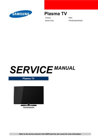
  • 1. Plasma TV Chassis F82A Model Code PS43D450A2WXZG SERVICEMANUAL Plasma TV PS43D450A2W Refer to the service manual in the GSPN (see the rear cover) for more information.
  • 2. 1. Precaution 1. Precaution To avoid possible damage, electric shocks or exposure to radiation, follow the instructions below with regard to safety, installation, service and ESD. 1.1. Safety Precautions 1) Make sure all protective devices are properly installed including non-metallic handles and compartment covers when installing or re-installing the chassis or chassis assemblies. 2) Make sure that no gaps exist between the cabinets for children to insert their fingers in to prevent children from receiving electric shocks. Gaps mentioned above include ventilation holes of a too great magnitude between the PDP module and the cabinet mask, and the improper installation of the rear cabinet. Errors may occur when the resistance is below 1.0MΩ or over 5.2MΩ. In these cases, make sure that the device is repaired before sending it back to the customer. 3) Check for Electricity Leakage (AC Leakage Test) WARNING Do not use an insulated transformer for checking the leakage. Use only those current leakage testers or mirroring systems that comply with ANSIC 101.1 and the Underwriter Laboratory’s specifications (UL1410, 59.7). DEVICE UNDER TEST LEAKAGE CURREN T TESTER TES T ALL EXPOSED ME TAL SUR FACES 2-WIRE CORD ALSO TES T WITH PLUG REVERSED (USING AC ADAPTER PLUG AS REQU IRED) EARTH GROUND ( R E A D I N G SHOULD NOT BE ABOVE 0.5mA) Figure 1.1 AC Leakage Test 4) A high voltage is maintained within the specified limits using safety parts, calibration and tolerances. When voltage exceeds the specified limits, check each special part. 5) Warning for Engineering Changes: Never make any changes or additions to the circuit design or the internal part for this product. Ex: Do not add any audio or video accessory connectors. This might cause physical damage. Furthermore, any changes or additions to the original design/engineering will invalidate the warranty. 6) Warning - Hot Chassis: Some TV chassis are directly connected to one end of the AC power cord for electrical reasons. Without insulated transformers, the product can only be repaired safely when the chassis is connected to the earthed end of the AC power source. To make sure the AC power cord is properly connected, follow the instructions below. Use the voltmeter to measure the voltage between the chassis and the earthed ground. If the measurement is over 1.0V, unplug the AC power cord and change the polarity before reinserting it. Measure the voltage between the chassis and the ground again. Copyright© 1995-2011 SAMSUNG. All rights reserved. 1-1
  • 3. 1. Precaution 7) Some TV chassis are shipped with an additional secondary grounding system. The secondary system is adjacent to the AC power line. These two grounding systems are separated in the circuit using an unbreakable/unchangeable insulation material. 8) When any parts, material or wiring appear overheated or damaged, replace them with new regular ones immediately. When any damage or overheating is detected, correct this immediately and make a regular check of possible errors. 9) Check for the original shape of the lead, especially that of the antenna wiring, any sharp edges, the AC power and the high voltage power. Carefully check if the wiring is too tight, incorrectly placed or loose. Never change the space between the part and the printed circuit board. Check the AC power cord for possible damages. Keep the part or the lead away from any heat-emitting materials. 10) Safety Indication: Some electrical circuits or device related materials require special attention to their safety features, which cannot be viewed by the naked eye. If an original part is replaced with another irregular one, the safety or protective features will be lost even if the new one has a higher voltage or more watts. Critical safety parts should be bracketed with ( , ). Use only regular parts for replacements (in particular, flame resistance and dielectric strength specifications). Irregular parts or materials may cause electric shock or fire. 1-2 Copyright© 1995-2011 SAMSUNG. All rights reserved.
  • 4. 1. Precaution 1.2. Servicing Precautions WARNING 1) First carefully read the “Safety Instruction” in this service manual. When there is a conflict between the service and the safety instructions, follow the safety instruction at all times. 2) Any electrolytic capacitor with the wrong polarity will explode. 1) The service instructions are printed on the cabinet, and should be followed by any service personnel. 2) Make sure to unplug the AC power cord from the power source before starting any repairs. a) Remove or re-install parts or assemblies. b) Disconnect the electric plug or connector, if any. c) Connect the test part in parallel with the electrolytic capacitor. 3) Some parts are placed at a higher position than the printed board. Insulated tubes or tapes are used for this purpose. The internal wiring is clamped using buckles to avoid contact with heat emitting parts. These parts are installed back to their original position. 4) After the repair, make sure to check if the screws, parts or cables are properly installed. Make sure no damage is caused to the repaired part and its surroundings. 5) Check for insulation between the blade of the AC plug and that of any conductive materials (i.e. the metal panel, input terminal, earphone jack, etc). 6) Insulation Check Process: Unplug the power cord from the AC source and turn the switch on. Connect the insulating resistance meter (500V) to the AC plug blade. The insulating resistance between the blade of the AC plug and that of the conductive material should be more than 1MΩ. 7) Any B+ interlock should not be damaged. If the metal heat sink is not properly installed, no connection to the AC power should be made. 8) Make sure the grounding lead of the tester is connected to the chassis ground before connecting to the positive lead. The ground lead of the tester should be removed last. 9) Beware of risks of any current leakage coming into contact with the high-capacity capacitor. 10) The sharp edges of the metal material may cause physical damage, so protect yourself by wearing gloves during the repair. 11) Due to the nature of plasma display panels, partial after-images may appear if a still picture is displayed on the screen for a long period of time. This is caused by brightness deterioration due to the storage effect of the panel, and to prevent this from happening, we recommend that the brightness and contrast are reduced. (e.g.) Contrast: 25, Brightness: 50 Copyright© 1995-2011 SAMSUNG. All rights reserved. 1-3
  • 5. 1. Precaution 1.3. Static Electricity Precautions 1) Some semi-conductive (“solid state”) devices are vulnerable to static electricity. These devices are known as ESD. ESD includes the integrated circuit and the field effect transistor. To avoid any materials damage from electrostatic shock, follow the instructions described below. 2) Remove any static electricity from your body by connecting the earth ground before handling any semi-conductive parts or assemblies. Alternatively, wear a dischargeable wrist-belt. (Make sure to remove any static electricity before connecting the power source - this is a safety instruction for avoiding electric shock) 3) Remove the ESD assembly and place it on a conductive surface such as aluminum foil to prevent accumulating static electricity. 4) Do not use any Freon-based chemicals. Such chemicals will generate static electricity that causes damage to the ESD. 5) Use only grounded-tip irons for soldering purposes. 6) Use only anti-static solder removal devices. Most solder removal devices do not support an anti-static feature. A solder removal device without an anti-static feature can store enough static electricity to cause damage to the ESD. 7) Do not remove the ESD from the protective box until the replacement is ready. Most ESD replacements are covered with lead, which will cause a short to the entire unit due to the conductive foam, aluminum foil or other conductive materials. 8) Remove the protective material from the ESD replacement lead immediately after connecting it to the chassis or circuit assembly. 9) Take extreme caution in handling any uncovered ESD replacements. Actions such as brushing clothes or lifting your leg from the carpet floor can generate enough static electricity to damage the ESD. CAUTION These servicing instructions are for use by qualified service personnel only. To reduce the risk of electric shock do not perform any servicing other than that contained in the operating instructions unless you are qualified to do so. 1-4 Copyright© 1995-2011 SAMSUNG. All rights reserved.
  • 6. 1. Precaution 1.4. Installation Precautions 1) For safety reasons a minimum of two people are required to carry this product. 2) Keep the power cord away from any heat emitting devices, as a melted covering may cause fire or electric shock. 3) Do not place the product in areas with poor ventilation such as a bookshelf or closet. The increased internal temperature may cause fire. 4) Bend the external antenna cable when connecting it to the product. This is a measure to protect it from being exposed to moisture. Otherwise, it may cause a fire or electric shock. 5) Make sure to turn the power off and unplug the power cord from the outlet before repositioning the product. Also check the antenna cable or the external connectors if they are fully unplugged. Damage to the cord may cause fire or electric shock. 6) Keep the antenna far away from any high-voltage cables and install it firmly. Contact with the high-voltage cable or the antenna falling over may cause fire or electric shock. 7) When connecting the RF antenna, check for a DTV receiving system and install a separate DTV reception antenna for areas with no DTV signal. 8) When installing the product, leave enough space (4”) between the product and the wall for ventilation purposes. A rise in temperature within the product may cause fire. 9) When moving a PDP with removable speakers, detach the speakers first before moving the main body. Moving the PDP main body without separating the speakers may cause the speakers to detach, possibly causing damage or injury. Copyright© 1995-2011 SAMSUNG. All rights reserved. 1-5
  • 7. 2. Product Specification 2. Product Specification 2.1. Product Feature ■ Features Block Specification Major IC Remark RF Digital/Analog (DTV Built In) PDP Module SDI DH MODULE 43” HD 51” HD New Module Power SAMSUNG ELECTRO MECHANICS SMPS DOYANG SMPS Video NTSC 3.58 ATSC HDMI Component, PC MSD 2248 Sound SRS TruSuround HD, Dolby Digital TAS 5715 Optical Output Cabinet C490 Design Copyright© 1995-2011 SAMSUNG. All rights reserved. 2-1
  • 8. 2. Product Specification ■ Specification Model P*43D4*0 P*51D4*0 Dimensions (W x H x D) 39.8 x 27.5 x 12 inches - with stand 39.8 x 24.5 x 2.2 inches - without stand 46.7 x 30.8 x 12 inches - with stand 46.7 x 27.8 x 2.2 inches - without stand Weight 41.8 lbs - with stand 35.2 lbs - without stand 56.2 lbs - with stand 49.6 lbs - without stand Panel Resolution 1024 x 768 1360 x 768 PC Resolution 1920 (H) x 1080 (V) Screen Size 43 Inches (16:9) 51 Inches (16:9) Power Consumption 43 HD: 200W ±10% and Less 51 HD : 280W ±10% and Less Antenna Input ANT - AIR / CABLE IN 75Ω unbalanced W/W AV COMPONENT1 - 480i / 480p / 720p / 1080i / 1080p COMPONENT2 - 480i / 480p / 720p / 1080i / 1080p PC HDMI1 – 480p / 720p / 1080i / 1080p HDMI2 (DVI Compatible) – 480p / 720p / 1080i / 1080p HDMI3 (SIDE AV) – 480p / 720p / 1080i / 1080p 480i can be displayed on HDMI, however it is not contained in EDID data. Video Input EU AV COMPONENT1 - 480i / 480p / 720p / 1080i / 1080p SCART - 21P, Sn, BLK PC HDMI1 – 480p / 720p / 1080i / 1080p HDMI2 (DVI Compatible) – 480p / 720p / 1080i / 1080p HDMI3 (SIDE AV) – 480p / 720p / 1080i / 1080p 480i can be displayed on HDMI, however it is not contained in EDID data. Audio Input AV COMPONENT 1 - 480i / 480p / 720p / 1080i / 1080p COMPONENT 2 - 480i / 480p / 720p / 1080i / 1080p PC DVI Audio Output AUDIO (L/R) Speaker Output 10W + 10W (40dB + 40dB) New Features 3D Built-In 2-2 Copyright© 1995-2011 SAMSUNG. All rights reserved.
  • 9. 2. Product Specification 2.2. Specifications Analysis Model P*43D4*0 P*51D4*0 P*42C450* Design Display Type PDP TV PDP TV PDP TV Built-In Tuner O O O Resolution 1024 x 768 1365 x 768 1024 x 768 PDP Module DH DH U2P Screen Size 43 inches 51 inches 42 inches Basic Picture ratio 16 : 9 16 : 9 16 : 9 Brightness 1,500 Cd/m2 1,500 Cd/m2 1,500 Cd/m2 Contrast Ratio 10,000 : 1 10,000 : 1 30,000 : 1Picture Picture Enhacer DNIe (SEMS20) DNIe (SEMS20) DNIe Equalizer 5 Band 5 Band 5 Band Auto Volume Control O O O Surround Sound SRS Theater Sound SRS Theater Sound SRS TruSurround HD Audio Speaker Output 10W + 10W 10W + 10W 10W + 10W PIP O O O Double Screen X X X Caption O O O Still Image X X X EPG O O O My color Control X X X Energy Saving O O O Screen Burn Protection O O O Features Anynet X X O Antenna 1 (Cable/Air) 1 (Cable/Air) 1 (Cable/Air) AV Input 1 Input 1 Input 1 Input S-Video X X X W/W 2 Input 2 Input 2 Input Component EU 1 Input 1 Input 1 Input PC (D-SUB) 1 Input 1 Input 1 Input DVI X X X HDMI D490 – 3 Input D450 – 2 Input D490 – 3 Input D450 – 2 Input 4 Input USB 1 1 1 Sub Woofer X X X Connections Optical 1 1 1 Etc. Speaker/Stand Built-in Speaker Built-in Speaker Built-in Speaker Copyright© 1995-2011 SAMSUNG. All rights reserved. 2-3
  • 10. 2. Product Specification TIP O : Supported, X : Not Supported NOTE For the power supply and power consumption, refer to the label attached to the product. 2-4 Copyright© 1995-2011 SAMSUNG. All rights reserved.
  • 11. 2. Product Specification 2.3. Accessories 2.3.1. Supplied Accessories Accessories Item Item code Remark A B C D Remote Control AA59-00484A Batteries 4301-000103 Power Cord 3903-000456 Owner`s Instructions BN68-03491C Cloth-Clean BN63-01798B Ferrite Core for Power Cord 3301-002049 Samsung Service Center Copyright© 1995-2011 SAMSUNG. All rights reserved. 2-5
  • 12. 2. Product Specification 2.3.2. Sold Separately Accessories Item Item code Remark RS232 Cable - HDMI - HDMI-DVI - Component - Composite (AV) - Coaxial (RF) - VGA - Samsung Service Center 2-6 Copyright© 1995-2011 SAMSUNG. All rights reserved.
  • 13. 3. Disassembly & Reassembly 3. Disassembly & Reassembly 3.1. Overall Disassembly & Reassembly CAUTION • Be sure to separate the power cord before disassembling the unit. • Discharge the capacitors first when separating PCB’s with high capacity capacitors such as SMPS, X Main Board, Y Main Board, etc. (A spark may be generated by the electric charge, and there is danger of electronic shock.) • Check that the cables are properly connected referring to the circuit diagram when disassembling or assembling the unit taking care not to damage the cables • Take care not to scratch the Glass Filter in the front. • Assemble the boards in the reverse order of the disassembly. • The plasma must be layed down on a flat padded surface for disassembly and reassembly. 1. Place monitor face down on cushioned table. Remove screws from the Stand. Remove stand. * Rear view of 43" <43" PDP> <43" PDP> 6001–002621 : M4 * L8 Copyright© 1995-2011 SAMSUNG. All rights reserved. 3-1
  • 14. 3. Disassembly & Reassembly * Rear view of 51" <51" PDP> <51" PDP> 6001–002621 : M4 * L8 2. Remove the screws of rear-cover. * Rear view of 43" <43" PDP> 6003–001782 : M4 * L12 6003–000337 : M4 * L10 * Rear view of 51" <51" PDP> 6003–001782 : M4 * L12 6003–000337 : M4 * L10 3-2 Copyright© 1995-2011 SAMSUNG. All rights reserved.
  • 15. 3. Disassembly & Reassembly 3. Lift up and remove the rear-cover. * Rear view of 43" <43" PDP> * Rear view of 51" <51" PDP> 4. Remove the screws of main board. CAUTION Disconnect all connectors prior to removing boards. 6001–002606 : M3 * L10 5. Remove the screws of SMPS. Remove the SMPS. CAUTION Align board under tab when re-installing. 6001–002606 : M3 * L10 6003–001439 : M4 * L8 6. Remove the speakers. (R/L) Copyright© 1995-2011 SAMSUNG. All rights reserved. 3-3
  • 16. 3. Disassembly & Reassembly 7. Remove the Cover Bottom. 8. Remove the screw of Bluetooth Module. NOTE PD49X Series Only. 6001–002606 : M3 * L10 9. Remove the screws of Bracket Stand Link. Lift up the Stand Bracket Stand Link. 6003–001782 : M4 * L12 6003–000337 : M4 * L10 10. Remove the screws of the front-cover. * Rear view of 43" <43" PDP> 6003–001782 : M4 * L12 * Rear view of 51" <51" PDP> 6003–001782 : M4 * L12 3-4 Copyright© 1995-2011 SAMSUNG. All rights reserved.
  • 17. 3. Disassembly & Reassembly 3.2. Method for Disassembly of Function Assy 1. Put up the upper Locking, Use screwdriver. 2. Put up the lower Locking, Use screwdriver. 3. Remove Locking. 4. Detach the Function PBA. CAUTION Disconnect all connectors prior to removing boards. Copyright© 1995-2011 SAMSUNG. All rights reserved. 3-5
  • 18. 4. Troubleshooting 4. Troubleshooting 4.1. Checkpoints by Error Mode 4.1.1. First Checklist for Troubleshooting 1) Check the various cable connections first. • Check to see if there is a burnt or damaged cable. • Check to see if there is a disconnected or loose cable connection. • Check to see if the cables are connected according to the connection diagram. 2) Check the power input to the Main Board. 3) How to distinguish if the problem is caused by Main board or Logic Board. • No Video : If the problem is No Video but Logic Board is on and Indication LED is blinking repeatedly and faster than normal booting, replace the T-Con board. • Distorted Picture : Check the inner patterns. Inner pattern Picture Problem OK NG Main board NG NG Main or LVDS cable or Logic Board or Panel. • How to check inner pattern? a. Factory mode (mute → 1 → 8 → 2 → Power on when TV is in ‘stand - by mode’ ) b. Move to SVC menu. c. Move to Test Pattern. d. Check inner patterns. Copyright© 1995-2011 SAMSUNG. All rights reserved. 4-1
  • 19. 4. Troubleshooting 4.1.2. Checkpoints by Error Mode ■ No Power Symptom • The LEDs on the front panel do not work when connecting the power cord. • The SMPS relay does not work when connecting the power cord. • The unit appears to be dead. Major Checklist The SMPS relay or the LEDs on the front panel does not work when connecting the power cord if the cables are improperly connected or the Main Board or SMPS is not functioning. In this case, check the following: • Check the internal cable connection status inside the unit. • Check the fuses of each part. • Check the output voltages of the SMPS. • Replace the Main Board. Diagnostics Fuse CN801 CN201 <43" PDP> Fuse CN801 CN201 <51" PDP> 4-2 Copyright© 1995-2011 SAMSUNG. All rights reserved.
  • 20. 4. Troubleshooting Yes Yes Yes Yes Power indicator LED is on? Check AC power connection. Replace the Main Board. Connect the cable between CN801 and CN201 connector. Are the SMPS CN801 and Main CN201 connected? Replace Fuse. (F801S) Is the Fuse(F801S) of the SMPS Power Input Part Open? Replace the SMPS. SMPS CN801 PIN2 : STB5V PIN1_ PS ON : Check to see if it is 0V? No No No No CAUTION Make sure to disconnect the power before working on the SMPS board. Copyright© 1995-2011 SAMSUNG. All rights reserved. 4-3
  • 21. 4. Troubleshooting ■ No Video Symptom • Audio is normal but no picture is displayed on the screen. Major Checklist • The output voltage of the Main SMPS. • This may happen when the LVDS cable connecting the Main Board and the Panel is disconnected. Diagnostics LVDS cable <43" PDP> LVDS cable <51" PDP> 4-4 Copyright© 1995-2011 SAMSUNG. All rights reserved.
  • 22. 4. Troubleshooting Check the LED Operation. Yes Yes Yes Replace the Main Board. Check / Replace the LVDS Cable. Check the LVDS connector. Is it connected correctly? Replace the SMPS. Check All output voltages on SMPS. Are all voltages normal? Replace the Logic Board. Check the LED operation of Logic Board whitch is normally operating? (Normal : Blink once a second) No No No CAUTION Make sure to disconnect the power before working on the SMPS board. Copyright© 1995-2011 SAMSUNG. All rights reserved. 4-5
  • 23. 4. Troubleshooting ■ No Sound Symptom • Video is normal but there is no sound. Major Checklist • When the speaker connectors are disconnected or damaged. • When the sound processing part of the Main Board is not functioning. • Speaker defect. • SMPS not supplying voltage to the main board. Diagnostics <43" PDP> Speaker Speaker cable CN801 <51" PDP> 4-6 Copyright© 1995-2011 SAMSUNG. All rights reserved.
  • 24. 4. Troubleshooting Yes Yes Yes Replace the Speaker. Replace the SMPS. Is the output voltage of SMPS normal? (CN801 7pin : 15V) Replace the Main board. (1) Is the speaker output terminal of the Main board normal? Connect the cable properly or replace the cable, if necessary. Is the cable connection between Main board and the speaker properly connected? No No No Sound OutputShape (1) CAUTION Make sure to disconnect the power before working on the IP board. Copyright© 1995-2011 SAMSUNG. All rights reserved. 4-7
  • 25. 4. Troubleshooting 4.1.3. Faults and Corrective Actions Symptom Related Image Causes and Countermeasures A blank vertical cell (block) appears on the screen. • Address buffer defect • Replace the corresponding upper/lower buffers. (E, F or G) • COF defect (burnt) • Replace the module. A green screen appears when the TV is turned on. • The Scale is not reseting. • Replace the Main board. The OSD box appears but there is no text. • Incorrect program version. • Check the version of each program. • Replace the Main board. A blank upper (or lower) block appears on the screen. • Upper/Lower Y Buffer defect • Replace the corresponding upper/ lower buffers. Either the main or sub picture does not appear. • Replace the Main board. A vertical green line appears on the screen. • The SMPS voltage is incorrect. • Adjust the SMPS voltage according to the voltage printed on the module label. 4-8 Copyright© 1995-2011 SAMSUNG. All rights reserved.
  • 26. 4. Troubleshooting Symptom Related Image Causes and Countermeasures Dim screen (blurred in red) • X-Main board defect • Replace the X-Main board. A blank screen appears. • Replace the Y-Main board. Copyright© 1995-2011 SAMSUNG. All rights reserved. 4-9
  • 27. 4. Troubleshooting 4.1.4. Operating Logic LED ■ Normal • LED ON/OFF for 0.5s OFF ON Power ON Logic ON Sequence (POS) Normal Toggling (every 32 Vsync) -. NT : 534 ms -. PAL : 640 ms ■ Abnormal • LED ON/OFF three times for 8.1s 540 ms 8.06 sec Exception 540 ms 540 ms 540 ms 540 ms 27Mhz 2.44 sec 163 ms PLL ON 163 ms 163 ms 163 ms 163 ms ··ªª µµ ªª ¦¦ ¹¹ee... ··ªª µµ ªª ¦¦ ¹¹ee... ■ DRV_RESET • LED ON for 5s and LED OFF for 2s 5 sec ··ªª µµ ªª ¦¦ ¹¹ee... DRV_RESET 2 sec 4-10 Copyright© 1995-2011 SAMSUNG. All rights reserved.
  • 28. 4. Troubleshooting 4.1.5. Adjust Function Key Sensitivity 1) Select 'Factory' 2) Select 'Control' Copyright© 1995-2011 SAMSUNG. All rights reserved. 4-11
  • 29. 4. Troubleshooting 3) Select 'Sub Option' 4) Select 'Key Sensitivity' 4-12 Copyright© 1995-2011 SAMSUNG. All rights reserved.
  • 30. 4. Troubleshooting 5) Default value (PD490=56, PD550=32) 6) Adjust The Value of Key Sensitivity No use 'Key Sens itivity' Very Sensitive Insensitive Copyright© 1995-2011 SAMSUNG. All rights reserved. 4-13
  • 31. 4. Troubleshooting 4.1.6. Function Assy Pin Map ■ US Main Board CN1201 Pinmap 1. IR 2. GND 3. A3.3V 4. SCL 5. SDA 6. FUNC_INTR 7. LED_STB ■ EU Main Board CN1201 Pinmap 1. IR 2. GND 3. A3.3V 4. SCL 5. SDA 6. FUNC_INTR 7. LED_STB 4-14 Copyright© 1995-2011 SAMSUNG. All rights reserved.
  • 32. 4. Troubleshooting 4.1.7. Adjust SMPS Voltage when change SMPS VS_TP VS_VR VA_TP VA_VR VS_TP VS_VR VA_TP VA_VR TIP • T.P : Test Point • V.R : Variable Resistor Copyright© 1995-2011 SAMSUNG. All rights reserved. 4-15
  • 33. 4. Troubleshooting 4.2. Factory Mode Adjustments 4.2.1. Entering Factory Mode To enter ‘Service Mode’ Press the remote-control keys in this sequence. • If you do not have Factory remote-control. ŸŸ ¾¾ ÆÆ ´´ ÁÁoožž •• •• oo ŸŸ ¾¾ ÆÆ ´´ ÁÁoožž ˜˜ •• žž œœ ””  ¤¤ oo”” ¤¤ œœ ¤¤ ££ ”” oo ŸŸ ¾¾ ÆÆ ´´ ÁÁoožž •• •• oo ŸŸ ¾¾ ÆÆ ´´ ÁÁoožž œœ ¤¤ ££ ”” oo¦¦ ~~ ¦¦ €€ ‡‡  • If you have Factory remote-control. INFO Factory • If you don’t have Factory remote control, can’t control some menu. Option Control SVC Expert ADC / WB Advanced T-MST4AUSC-0408.0 T-MST4AUSS-0019 E-Manual : X6ATSCA-0003 EDID SUCCESS HDCP SUCCESS CALIB : AV O COMP O PC O HMDI O Option : 2701, 1374 SDAL-0.58.1.0 RFS : "Mstar-X5 0039" KERNEL MODULE VERSION: "00035_90" 2010-12-08 Type : 51DFHcD Model : PN51D550 MAC SUCCESS LOCD X Factory Data Ver : 68 EERC Version : 501 DTP-AP-COMP-582 DTP-BP-HAL-0083 DTP-BP-0582 Date of purchase : mm/dd/yyyy 4-16 Copyright© 1995-2011 SAMSUNG. All rights reserved.
  • 34. 4. Troubleshooting 4.2.2. Factory Data ■ Option Item Data Remark Factory Reset - Type 43DHHcD Local Set xx Model PD490 Tuner xx Ch table NONE Front Color T-R-BLK ■ Control Menu Item Data Remark EDID EDID ON/OFF ON EDID WRITE ALL Success EDID WRITE PC Success EDID WRITE HDMI ... EDID WRITE HDMI1 Success EDID WRITE HDMI2 Success EDID WRITE HDMI3 Success EDID WRITE HDMI4 Success HDMI EDID Ver HDMI 1.2 HDMI EDID Port NONE EDID WRITE DVI ... Sub Option RF Mute Time 600ms RS-232 Jack Debug Watchdog OFF WD COUNT 255 Dimm Type LVDS FORMAT PDP Language_Arabic xx TOOLS Support 32 LNA Support 0 DB On with 5MB MOVIE chapterinmed DLNA ON MediaPlay Play List OFF NETWORK Support Ext-Wifi Info Link Server Type development Copyright© 1995-2011 SAMSUNG. All rights reserved. 4-17
  • 35. 4. Troubleshooting Menu Item Data Remark Info Link Country None TTX List TTX Group 24Px4 Support OFF Power Indicator Support OFF BD Wise Support OFF Data Service Support OFF OTA Duration Test OFF Alternate Del OFF OTN Server Type operating OTN Test Server OFF OTN Support ON OTN Reset OTN Duration OFF OTN Fail Test OFF IIC BUS STOP OFF Visual Test Disable Emergency Log Copy Checksum 0x0000 Select Log Type IR KEY Log View View Log Delete Log ColorSpace Support RGB Type Gemstar On/Off OFF WSS Support OFF PVR Support OFF CI Support OFF Eepron Reset LVDS Spread ON Period 40K Amplitude 1.5 Spread Spectrum DDR Spread 1.0% Spread A CTRL_OFFSET_0_3 0x0 A CTRL_OFFSET_D 0x0 B CTRL_OFFSET_0_3 0x0 DDR Margin B CTRL_OFFSET_D 0x0 H.264 Margin 8 MPEG Margin 1000 Tuner Margin 10 4-18 Copyright© 1995-2011 SAMSUNG. All rights reserved.
  • 36. 4. Troubleshooting Menu Item Data Remark Y0 Ref 165 Y1 Ref 148 Y2 Ref 119 Y3 Ref 101 Y4 Ref 76 Y5 Ref 60 Y6 Ref 31 Y7 Ref 0 Cb0 Ref 128 Cb1 Ref 64 Cb2 Ref 148 Cb3 Ref 85 Cb4 Ref 171 Cb5 Ref 108 Cb6 Ref 194 Cb7 Ref 0 Cr0 Ref 128 Cr1 Ref 137 Cr2 Ref 64 Cr3 Ref 74 Cr4 Ref 181 Cr5 Ref 192 Cr6 Ref 118 SST Cr7 Ref 0 Y0 TH 20 Y1 TH 20 Y2 TH 20 Y3 TH 20 Y4 TH 20 Y5 TH 20 Y6 TH 20 Y7 TH 20 Cb0 TH 20 Cb1 TH 20 Cb2 TH 20 Cb3 TH 20 Cb4 TH 20 Cb5 TH 20 Cb6 TH 20 Cb7 TH 20 SST_TH Copyright© 1995-2011 SAMSUNG. All rights reserved. 4-19
  • 37. 4. Troubleshooting Menu Item Data Remark Cr0 TH 20 Cr1 TH 20 Cr2 TH 20 Cr3 TH 20 Cr4 TH 20 Cr5 TH 20 Cr6 TH 20 Cr7 TH 20 2nd mips ON 2nd mips count 0 Region xxx PnP Language xxx PC Auto Ident Enable OTP Lock ... Auto Power MEMORY KEY SENSITIVITY 56 1(Very Sensitive)~255(Insensitive) FANET OFF OTA Support OFF WIFI REGION V FKP Down PDP Option LOGIC CONNECT OFF PIXEL SHIFT TEST OFF PANEL VERSION DF PANEL INCH 51FHD PANEL TYPE 53 PANEL TEMPERATURE 40 LOGIC ID A712 LOGIC SW VERSION 2010-11-20 LOGIC SW CHECKSUM 0xFC31 MRT 44 SAPC TIMER ON APC SPEED SLOW Real 100 Hz Support OFF XGA Resolution OFF PLG_SHOP 128 Hotel Option HOTEL MODE ON POWER ON CHANNEL EN User Defined POWER ON CHANNEL 3 CHANNEL TYPE CATV 4-20 Copyright© 1995-2011 SAMSUNG. All rights reserved.
  • 38. 4. Troubleshooting Menu Item Data Remark POWER ON VOLUME EN User Defined POWER ON VOLUME 10 MIN VOLUME 0 MAX VOLUME 100 PANEL BUTTON LOCK Unlock POWER ON SOURCE TV Picture Menu Lock OFF Music Mode AV OFF Music Mode PC OFF Music Mode Comp OFF Music Mode Backlight OFF Menu Display ON Power On Option Last Option Auto Source OFF Energy Saving OFF Clone TV to USB Clone USB to TV Setting Auto initialize OFF SIRCH Update Time 2:00 AM MONITOR OUT CVBS ON Shop Option Shop Mode OFF Exhibition Mode OFF Asia Option TTX OFF China HD OFF NT Conversion OFF Sepco 120Hz OFF Unbalance OFF FMTransmitter Support OFF FMTransmitter Carrier OFF AF Level adjust 3 TX power Level 0 Mono Last Memory OFF H Shaking OFF SOUND High Devi OFF Carrier Mute ON Volume Curve Type1 Speaker Delay Normal 50 Pilot Level High Thld 0x28h Pilot Level Low Thld 0x10h FM Prescale 0 Copyright© 1995-2011 SAMSUNG. All rights reserved. 4-21
  • 39. 4. Troubleshooting Menu Item Data Remark AM Prescale 0 NICAM Prescale 0 Amp Volume 0xc7h Amp Scale 0x82h Woofer Type 1 Woofer Scale 0x7fh Woofer Check Sum Speaker EQ ON Amp Model 0 Speaker cut-off Freq NTP7411 SPDIF PCM Gain -9 dB FM M Prescale 48 BTSC Mono Prescale 25 BTSC stereo Prescale 47 SAP Prescale 43 A2 Ident High Thld 31 A2 Ident Low Thld 2 Carrier2 Amp High Thld 4 Carrier2 Amp Low Thld 3 Carrier2 SNR High THR 16 Carrier2 SNR Low THR 80 Audio-IP Test Ready TruBass-Checksum 0x200190E2 PWM Mode BD Config Option Num of ATV 1 Num of DTV 1 Num of AV 1 Num of SVIDEO 0 Num of COMP 2 Num of HDMI 4 Num of PC 1 Num of SCART 0 Num of DVI 0 Num of OPTICAL Link 0 Num of MEDIA 1 Num of PANEL KEY 6 Num of USB Port 2 Num of HeadPhone 0 4-22 Copyright© 1995-2011 SAMSUNG. All rights reserved.
  • 40. 4. Troubleshooting Menu Item Data Remark Num of RVU 0 MFT Offset 62.5 Select LCD/PDP PDP HDMI/DVI SEL 1 Indicator Led OFF Wall Mount OFF HV Flip OFF Num Of Display 2 DVI/HDMI SOUND Auto HDMI HOT PLUG Disable HOTPLUG SWITCHING Boot HOT PLUG DURATION 1200ms CLK TERM DURATION 1200ms HDMI FLT CNT SIG 100ms HDMI FLT CNT LOS 100ms UNSTABLE BAN CNT 3500ms HDMI Err Cnt 1 HDMI ROBIN ON HDMI Callback OFF HDMI CTS Thld 8 HDMI CTS Cnt1 1 TMDS_EQ2_Boost 1 TMDS_EQ2_Gain 0 TMDS_PLL_Loop 3 TMDS_CPREG_BLEED 1 HDMI EQ Auto HDMI EDID wRITE Type Separate HDMI Switch NONE DVI SET TIME 300ms Type Of PANEL KEY PDPVertical EcoSensor Support ON LEDMotionPlus Support OFF Natural Mode Support OFF All Share Support ON Copyright© 1995-2011 SAMSUNG. All rights reserved. 4-23
  • 41. 4. Troubleshooting Menu Item Data Remark Relax Mode Support OFF DVI-I Support Melfas Function Support Light Level Support H Write HDMI Sync DE HeadPhone Port A Out2 SCC SCC Mode Dynamic SCC ON/OFF OFF Hx 272 Hy 278 Lx 272 SCC Input Data Ly 278 sSCC Hx 550 sSCC Hy 566 sSCC Lx 598 sSCC Const sSCC Ly 550 pSCC Hx 550 pSCC Hy 566 pSCC Lx 598 pSCC Const pSCC Ly 550 SCC Source Data PBA SWAP PBA 4-24 Copyright© 1995-2011 SAMSUNG. All rights reserved.
  • 42. 4. Troubleshooting ■ SVC Menu Item Data Remark Test Pattern Pattern Sel ... LOGIC Pattern Sel 0 LOGIC Level Sel 255 Panel Auto Setting Failure PANEL DISPLAY TIME 2Hr LOGIC USB D/L off Tuner Status T-CON USB Download Failure MICOM UPGRADE Off BT ADDRESS e4e0c53197db BT UPGRADE SVC Reset ■ Expert Menu Item Data Remark N/D ADJ OFF Source ... ■ ADC/WB Menu Item Data Remark ADC AV Calibration Comp Calibraion PC Calibration HDMI Calibration ADC Target 1st_AV_Low 64 1st_AV_High 880 1st_AV_Delta 2 1st_COMP_Y_Low 64 1st_COMP_Cb_Low 512 1st_COMP_Cr_Low 512 1st_COMP_Y_High 940 1st_COMP_Cb_High 512 1st_COMP_Cr_High 512 1st_COMP_Delta 2 1st_PC_Low 4 1st_PC_High 1004 Copyright© 1995-2011 SAMSUNG. All rights reserved. 4-25
  • 43. 4. Troubleshooting Menu Item Data Remark 1st_PC_Delta 2 2nd_ACH_Low 4 2nd_ACH_High 940 2nd_PC_Low 4 2nd_PC_High 940 2nd_Delta 2 ADC Result 1st_Y_GH 258 1st_Y_GL 128 1st_Cb_BH 1st_Cb_BL 1st_Cr_RH 1st_Cr_RL 2nd_R_L 133 2nd_G_L 133 2nd_B_L 133 2nd_R_H 70 2nd_G_H 70 2nd_B_H 70 White Balance Sub Brightness 128 R-Offset 128 G-Offset 128 B-Offset 128 Sub Contrast 128 R-Gain 128 G-Gain 128 B-Gain 128 Movie R-Offset Movie B-Offset Movie R-Gain Movie B-Gain ■ Advanced • Picture_2D Menu Item Data Remark Sub Setting Gamma 0.95 Natural Gamma 0 Pwm Max 100 PWM Min 0 Pwm Mid 0 Contrast Dimming OFF 4-26 Copyright© 1995-2011 SAMSUNG. All rights reserved.
  • 44. 4. Troubleshooting Menu Item Data Remark 7.5 IRE NTSC OFF 7.5 IRE Offset Comp Phase 110 Led Peak OnOff OFF Dither Bypass OFF D Motion Light On Dynamic Contrast On EPA Standard Standard Contrast 100 Standard Brightness 45 Standard Sharpness 50 Standard Color 50 Standard Tint 0 Standard Backlight 10 WB Movie W/B Movie On/Off OFF Model ... Color Tone ... Msub Brightness ... Msub Contrast ... N_Rgain ... N_Bgain ... N_Roffset ... N_boffset ... W2_Rgain ... W2_Bgain ... W2_Roffset ... W2_Boffset ... Movie Contrast ... Movie Bright ... Movie Color ... Movie Sharpness ... Movie Tint ... Movie Backlight ... Movie Gamma ... M_Sub_Gamma ... HDMI Black Level ... WCE WRHue 64 WRSat 16 WYHue 64 WYSat 16 WGHue 64 Copyright© 1995-2011 SAMSUNG. All rights reserved. 4-27
  • 45. 4. Troubleshooting Menu Item Data Remark WGSat 16 WCHue 64 WCSat 16 WBHue 64 WBSat 16 WMHue 64 WMSat 16 ARHue 64 ARSat 16 AYHue 64 AYSat 16 AGHue 64 AGSat 16 ACHUE 64 ACSat 16 ABHue 64 ABSat 16 AMHue 64 AMSat 16 VDEC AGC mode 3 AGC manual gain 72 Ifcomptype 1 Ifcompsel 15 Saturain Cb/Cr 145 Secam Filter Sel 0 RGB Delay 150 Peaking Gain 0 Coring Gain 3 Chroma Peak 10 2D V Peaking 0 2D H Peaking 0 2D Peaking Gain 0 Sharpness Post_H1 20 Post_H2 26 Post_H3 20 Post_H4 15 Post_v1 20 Post_v2 18 Post_H2 Overshoot 128 Post_H2 Undershoot 128 4-28 Copyright© 1995-2011 SAMSUNG. All rights reserved.
  • 46. 4. Troubleshooting Menu Item Data Remark Post_H3 Overshoot 128 Post_H3 undershoot 128 Core Gain1 2 CoreGain2 3 D_Tot_Gain 24 S_Tot_Gain 24 ColorMapping A_Red_R 60 A_Red_G 0 A_Red_B 0 A_Green_R 67 A_Green_G 100 A_Green_B 0 A_Blue_R 0 A_Blue_G 49 A_Blue_B 100 A_Yellow_R 100 A_Yellow_G 100 A_Yellow_B 0 A_Cyan_R 0 A_Cyan_G 46 A_Cyan_B 100 A_Magenta_R 27 A_Magenta_G 0 A_Magenta_B 67 N_Red_R 50 N_Red_G 0 N_Red_B 0 N_Green_R 0 N_Green_G 50 N_Green_B 0 N_Blue_R 0 N_Blue_G 0 N_Blue_B 50 N_Yellow_R 50 N_Yellow_G 50 N_Yellow_B 0 N_Cyan_R 0 N_Cyan_G 50 N_Cyan_B 50 N_Magenta_R 50 Copyright© 1995-2011 SAMSUNG. All rights reserved. 4-29
  • 47. 4. Troubleshooting Menu Item Data Remark N_Magenta_G 0 N_Magenta_B 50 Enhance BLE_Gain 22 D Sub Color 80 D Skin Hue 84 D Skin Sat 18 S Sub Color 80 S Skin Hue 72 S Skin Sat 16 M Sub Color 55 M Skin Hue 64 M Skin Sat 16 Sub Tint 45 CE_Normal_Left_Gain 35 CE_Normal_Right_Gain 20 CE_Normal_Offset -10 CE_Special_Left_Gain 15 CE_Special_Right_Gain 10 CE_Special_Offset -50 CE_S_Left_gain 10 CE_S_Right_Gain 40 CE_S_Normal_Offset -2 LNA_Plus Synctip_Noise 102 dB01_th 3 dB12_th 4 dB23_th 6 dB34_th 8 dB45_th 10 dB56_th 12 dB67_th 15 dB78_th 28 LNA_Plus_Yfiller 3 YC_Delay RF PAL BG 10 RF PAL DK 11 RF PAL I 13 RF PAL M 6 RF PAL n 11 RF SECAM BG 5 RF SECAM DK 8 RF SECAM L 8 4-30 Copyright© 1995-2011 SAMSUNG. All rights reserved.
  • 48. 4. Troubleshooting Menu Item Data Remark RF NT 358 14 RF NT 443 8 AV PAL 9 AV PAL M 7 AV PAL N 9 AV SECAM 9 AV NT 358 10 AV NT 443 4 AV Pal 60 6 SCART PAL 9 SCART PAL M 9 SCART PAL N 9 SCART SECAM 4 SCART NT 358 10 SCART NT 443 4 SCART PAL 60 6 SCART RGB PAL 8 SCART RGB PAL M 8 SCART RGB PAL N 8 SCART RGB SECAM 8 SCARTRGB NT 358 8 SCARTRGB NT 443 8 SCARTRGB PAL 60 8 Picture Update • Picture_3D Menu Item Data Remark Sub Setting_3D 3D_Gamma 0.95 3D_Natural Gamma 0 3D_Pwm Max 100 3D_PWM Min 0 3D_Pwm Mid 0 3D_Contrast Dimming OFF 3D_Led Peak OnOff OFF 3D_Dither Bypass OFF 3D_D Motion Light OFF 3D_Dynamic Contrast OFF EPA_3D 3D Contrast 100 Copyright© 1995-2011 SAMSUNG. All rights reserved. 4-31
  • 49. 4. Troubleshooting Menu Item Data Remark 3D Brightness 45 3D Standard Sharpness 50 3D Standard Color 50 3D Standard Tint 0 3D Standard Backlight 7 WB Movie_3D 3D_W/B Movie On/Off OFF 3D_Model ... 3D_Color Tone ... 3D_Msub Brightness ... 3D_Msub Contrast ... 3D_C_Rgain ... 3D_C_Bgain ... 3D_C_Roffset ... 3D_C_boffset ... 3D_N_Rgain ... 3D_N_Bgain ... 3D_N_Roffset ... 3D_n_Boffset ... 3D_W2_Rgain 3D_W2_Bgain 3D_W2_Roffset 3D_W2_Boffset 3D_Movie Contrast ... 3D_Movie Bright ... 3D_Movie Color ... 3D_Movie Sharpness ... 3D_Movie Tint ... 3D_Movie Backlight ... 3D_Movie Gamma ... 3D_M_Sub_Gamma ... 3D_HDMI Black Level ... 3D_Sub Contrast 128 3D_Sub_Brightness 128 WCE_3D 3D_WRHue 64 3D_WRSat 17 4-32 Copyright© 1995-2011 SAMSUNG. All rights reserved.
  • 50. 4. Troubleshooting Menu Item Data Remark 3D_WYHue 72 3D_WYSat 17 3D_WGHue 47 3D_WGSat 17 3D_WCHue 58 3D_WCSat 17 3D_WBHue 54 3D_WBSat 18 3D_WMHue 64 3D_WMSat 17 3D_ARHue 64 3D_ARSat 16 3D_AYHue 64 3D_AYSat 16 3D_AGHue 64 3D_AGSat 16 3D_ACHUE 64 3D_ACSat 16 3D_ABHue 64 3D_ABSat 16 3D_AMHue 64 3D_AMSat 16 ColorMapping_3D 3D_A_Red_R 50 3D_A_Red_G 0 3D_A_Red_B 0 3D_A_Green_R 0 3D_A_Green_G 50 3D_A_Green_B 0 3D_A_Blue_R 0 3D_A_Blue_G 0 3D_A_Blue_B 50 3D_A_Yellow_R 50 3D_A_Yellow_G 50 3D_A_Yellow_B 0 3D_A_Cyan_R 0 3D_A_Cyan_G 50 3D_A_Cyan_B 50 3D_A_Magenta_R 50 3D_A_Magenta_G 0 3D_A_Magenta_B 50 Copyright© 1995-2011 SAMSUNG. All rights reserved. 4-33
  • 51. 4. Troubleshooting Menu Item Data Remark 3D_N_Red_R 50 3D_N_Red_G 0 3D_N_Red_B 0 3D_N_Green_R 0 3D_N_Green_G 50 3D_N_Green_B 0 3D_N_Blue_R 0 3D_N_Blue_G 0 3D_N_Blue_B 50 3D_N_Yellow_R 50 3D_N_Yellow_G 50 3D_N_Yellow_B 0 3D_N_Cyan_R 0 3D_N_Cyan_G 50 3D_N_Cyan_B 50 3D_N_Magenta_R 50 3D_N_Magenta_G 0 3D_N_Magenta_B 50 Sharpness_3D 3D_Post_H1 16 3D_Post_H2 10 3D_Post_H3 10 3D_Post_H4 10 3D_Post_v1 20 3D_Post_v2 14 3D_Post_H2 Overshoot 32 3D_Post_H2 Undershoot 32 3D_Post_H3 Overshoot 16 3D_Post_H3 undershoot 16 3D_Core Gain1 1 3D_CoreGain2 2 3D_D_Tot_Gain 28 3D_S_Tot_Gain 28 Enhance_3D 3D_BLE_Gain 22 3D_D Sub Color 65 3D_D Skin Hue 100 3D_D Skin Sat 18 3D_S Sub Color 65 4-34 Copyright© 1995-2011 SAMSUNG. All rights reserved.
  • 52. 4. Troubleshooting Menu Item Data Remark 3D_S Skin Hue 72 3D_S Skin Sat 16 3D_M Sub Color 55 3D_M Skin Hue 64 3D_M Skin Sat 16 3D_Sub Tint 50 3D_CE_Normal_Left_Gain 20 3D_CE_Normal_Right_Gain 30 3D_CE_Normal_Offset -10 3D_CE_Special_Left_Gain 15 3D_CE_Special_Right_Gain 10 3D_CE_Special_Offset -50 3D_CE_S_Left_gain 10 3D_CE_S_Right_Gain 40 3D_CE_S_Normal_Offset -2 3D Setting BTPairDis_Ho 2 BTPairDis_sh 25 BTTransDis 10 BTSlaveDelay48 0 BTSlaveDelay50 0 BTSlaveDelay60 0 BTEmiDel_48 0 BTEmiDel_50 0 BTEmiDel_60 0 BTGlsDUTY 100 IREmiDel_48 0 IREmiDel_50 0 IREmiDel_60 0 IREmiMask 1 IRMASKPRD 1 IREmiNum 1 SlavDelay48 0 SlavDelay50 0 LED_BT_IR SlavDelay60 0 Copyright© 1995-2011 SAMSUNG. All rights reserved. 4-35
  • 53. 4. Troubleshooting Menu Item Data Remark BTPairDis_Ho_PDP 2 BTPairDis_sh_PDP 25 BTTransDis_PDP 10 BTSlaveDelay48_D 0 BTSlaveDelay50_D 0 BTSlaveDelay60_D 0 BTGlsDUTY_D 100 BTEmiDel_48_S 0 BTEmiDel_50_S 0 BTEmiDel_60_S 0 BTGlsDUTY_S 100 IREmiDel_48_R 0 IREmiDel_50_R 0 IREmiDel_60_R 0 BTGlsDUTY_R 100 BTEmiDel_48_M 0 BTEmiDel_50_M 0 BTEmiDel_60_M 0 BTGlsDUTY_M 100 IREmiMask_PDP 1 IRMASKPRD_PDP 1 IREmiNum_PDP 1 SlavDelay48_PDP 0 SlavDelay50_PDP 0 PDP_BT_IR SlavDelay60_PDP 0 PDuty192 25 PDuty200 25 PDuty240_Dyn 25 Duty PDuty210_Mov 25 Glmit_LBT0 88 Glmit_LBT1 89 Glmit_LBT2 90 Glmit_LBT3 91 Glmit_LLT0 95 Glmit_LLT1 96 Glmit_LLT2 97 Glmit_LLT3 98 DCCX1 0 DCCX2 0 DCCX3 0 Dcc 4-36 Copyright© 1995-2011 SAMSUNG. All rights reserved.
  • 54. 4. Troubleshooting Menu Item Data Remark DCCY1 0 DCCY2 0 DCCH1 0 DCCH2 0 DCCH3 0 DCCV1 0 DCCV2 0 Temp Read 0 Time_HOT 120 Time_Cold 120 Temp_ST 16 Temp_TH 40 delta 5 Depth_Min 10 Depth_Max 100 Viewp_Min_2D3D 64 Viewp_Max_2D3D 192 Viewpoint_Min 64 Effect viewpoint_Max 192 Debug OFF DccMode 0 DccSele0_0 0 DccSele0_1 0 DccSele0_2 0 DccSele0_3 0 DccSele0_4 0 DccSele0_5 0 DccSele0_6 0 DccSele0_7 0 PosiSel_0_0 0 PosiSel_0_1 0 PosiSel_0_2 0 PosiSel_0_3 0 PosiSel_0_4 0 PosiSel_0_5 0 PosiSel_0_6 0 PosiSel_0_7 0 PosiSel_0_8 0 PosiSel_0_9 0 PosiSel_0_10 0 Debug Copyright© 1995-2011 SAMSUNG. All rights reserved. 4-37
  • 55. 4. Troubleshooting Menu Item Data Remark PosiSel_0_11 0 Bypass OFF 4-38 Copyright© 1995-2011 SAMSUNG. All rights reserved.
  • 56. 4. Troubleshooting 4.3. Service Adjustment - You must perform Calibration in the Lattice Pattern before adjusting the White Balance. ■ White Balance - Calibration • Factory ADC / WB AV Calibration Comp Calibration PC Calibration HDMI Calibration ■ Color Calibration • Adjust spec. 1) Source : HDMI 2) Setting Mode : 1280*720@60Hz 3) Pattern : Pattern #24 (Chess Pattern) 4) Use Equipment : CA210 & Master MSPG925 Generator Use other equipment only after comparing The result with that of The Master equipment. Input mode Calibration Pattern CVBS IN (Model_#1) Perform in NTSC/PAL B&W Pattern #24 Lattice Component IN (Model_#6) Perform in 720p B&W Pattern #24 Lattice PC Analog IN (Model_#21) Perform in VESA XGA (1024x768) B&W Pattern #24 Lattice HDMI IN Perform in 720p B&W Pattern #24 Lattice Copyright© 1995-2011 SAMSUNG. All rights reserved. 4-39
  • 57. 4. Troubleshooting • Method of Color Calibration (AV) 1) Apply the NTSC/PAL Lattice (N0. 3) pattern signal to the AV IN 1 port. 2) Press the Source key to switch to “AV1” mode. 3) Enter Service mode. 4) Select the “ADC” menu. 5) Select the “AV Calibration” menu. 6) In “AV Calibration Off” status, press the “ ” key to perform Calibration. 7) When Calibration is complete, it returns to the high-level menu. 8) You can see the change of the “AV Calibration” status from Failure to Success. • Method of Color Calibration (Component) 1) Apply the 720p Lattice (N0. 6) pattern signal to the Component IN 1 port. 2) Press the Source key to switch to “Component1” mode. 3) Enter Service mode. 4) Select the “ADC” menu. 5) Select the “Comp Calibration” menu. 6) In “Comp Calibration Off” status, press the “ ” key to perform Calibration. 7) When Calibration is complete, it returns to the high-level menu. 8) You can see the change of the “Comp Calibration” status from Failure to Success. • Method of Color Calibration (PC) 1) Apply the VESA XGA Lattice (N0. 21) pattern signal to the PC IN port. 2) Press the Source key to switch to “PC” mode. 3) Enter Service mode. 4) Select the “ADC” menu. 5) Select the “PC Calibration” menu. 6) In “PC Calibration Off” status, press the “ ” key to perform Calibration. 7) When Calibration is complete, it returns to the high-level menu. 8) You can see the change of the “PC Calibration” status from Failure to Success. 4-40 Copyright© 1995-2011 SAMSUNG. All rights reserved.
  • 58. 4. Troubleshooting • Method of Color Calibration (HDMI) 1) Apply the 720p Lattice (N0. 6) pattern signal to the HDMI1/DVI IN port. 2) Press the Source key to switch to “HDMI1” mode. 3) Enter Service mode. 4) Select the “ADC” menu. 5) Select the “HDMI Calibration” menu. 6) In “HDMI Calibration Off” status, press the “ ” key to perform Calibration. 7) When Calibration is complete, it returns to the high-level menu. 8) You can see the change of the “HDMI Calibration” status from Failure to Success. ■ White Balance - Adjustment ADC / WB - White Balance Factory (Low light) (High light) Sub Bright R offset G offset B offset Sub Contrast R gain G gain B gain Copyright© 1995-2011 SAMSUNG. All rights reserved. 4-41
  • 59. 4. Troubleshooting 4.4. Software Upgrade Samsung may offer upgrades for the TV’s firmware in the future. These upgrades can be performed via the TV when it is connected to the Internet, or by downloading the new firmware from samsung.com to a USB memory device. • Alternative Software (Backup) shows The previous version that will be replaced. • Software is represented as ‘Year/Month/Day_Version’. The more recent the date, the newer the software version. Installing the latest version is recommended. ■ By USB Insert a USB drive containing the firmware upgrade downloaded from samsung.com into the TV. Please be careful to not disconnect the power or remove the USB drive while upgrades are being applied. The TV will turn off and turn on automatically after completing the firmware upgrade. Please check the firmware version after the upgrades are complete (the new version will have a higher number than the older version). have a higher number than the older version) made will return to their default (factory) settings. We recommend you write down your settings so that you can easily reset them after the upgrade. 4-42 Copyright© 1995-2011 SAMSUNG. All rights reserved.
  • 60. 4. Troubleshooting ■ By Online Upgrades the software using the Internet. • First, configure your network. For detailed procedures on using the Network Setting. Refer to the ‘Setting the Network’ instructions. • If The internet connection doesn’t operate properly, connection can be broken, please retry downloading. If the problem still happens, download by USB and upgrade. ■ Alternative Software (Backup) If there is an issue with the new firmware and it is affecting operation, you can change the software to the previous. • If Software was changed, existing Software is displayed. • You can change current Software to Alternative Software by ‘Alternative Software’. Copyright© 1995-2011 SAMSUNG. All rights reserved. 4-43
  • 61. 5. Wiring Diagram 5. Wiring Diagram 5.1. Overall Wiring ■ 43" HD Overall Wiring CN5500 CN5501 CN5502 CN5503 CN5504 CN5505 CN5009 CN5010 CN5011 Y-DRIVE SMPS X-DRIVE MAIN BOARD LOGIC BOARD E-BUFFER CN4000 CN4002 FUNCTIONBLUETOOTH SPEAKER CN5003 CN5000 CN800S CN5002 CN5001 CN804 CN801 CN802 CNXX CN4004 CN2501 CN2500 CN2600 CN2502 CN2601 CN201 CN1201 CN1602_HD CN302 CN1 F-BUFFER CN603_3DCN2021CN2001 CN2010 CN2009 CN2023CN2022 1 2 3 4 5 6 7 .. ‘‘ ›› ¤¤ ”” ££ žž žž ££ —— oo‰‰ooŸŸ ““ ƒƒ ˆˆ §§ oo¢¢ ´´ ÁÁ¸¸´´  oožž ½½ »»ÈÈ }}oo Copyright© 1995-2011 SAMSUNG. All rights reserved. 5-1
  • 62. 5. Wiring Diagram ■ 51" HD Overall Wiring CN5505 CN5504 CN5503 CN5500 CN5501 CN5502 CN5002 CN5004 CN5003 CN5005 Y-DRIVE X-DRIVE SMPS MAIN BOARD LOGIC BOARD E-BUFFER CN4906 CN4404 CN4406 CN4904 FUNCTIONBLUE TOOTH SPEAKER CN5001 CN5000 CN800S CN5006 CN5007 CN804 CN801 CN802 CN4701 CN4001 CN2501 CN2500 CN2600 CN2502 CN2601 CN201 CN1201 CN1602_HD CN302 CN1 F-BUFFER CN603_3DCN2021CN2002 CN2010 CN2011 CN2023CN2022 1 2 3 4 5 6 7 .. ‘‘ ›› ¤¤ ”” ££ žž žž ££ —— oo‰‰ooŸŸ ““ ƒƒ ˆˆ §§ oo¢¢ ´´ ÁÁ¸¸´´  oožž ½½ »»ÈÈ }}oo 5-2 Copyright© 1995-2011 SAMSUNG. All rights reserved.
  • 63. 5. Wiring Diagram NOTE The code number of cable (Lead-connector) can be changed, see “Exploded Views and Parts List”. ■ 43" Cable (Lead-connector) Use (1) POWER 12 Pin (7) LVDS FFC 51 Pin Code BN39-01285K BN96-13325G Photo ■ 51" Cable (Lead-connector) Use (1) POWER 12 Pin (7) LVDS FFC 51 Pin Code BN39-01285L BN96-13325F Photo Copyright© 1995-2011 SAMSUNG. All rights reserved. 5-3
  • 64. 5. Wiring Diagram 5.1.1. Pin Connection (1) CN801 (SMPS) ↔ CN201 (Main Board) Pin No. (SMPS) Signal (SMPS) Pin No. (Main Board) Signal (Main Board) 1 PS-ON 1 SW_POWER 2 STBY 2 A5V_PW 3 GND 3 DGND 4 D15V 4 B15VS_PW 5 GND 5 DGND 6 GND 6 DGND 7 D5.3V 7 B5V_PW 8 D5.3V 8 B5V_PW 9 GND 9 DGND 10 D15V 10 B15V_PW 11 D15V 11 B15V_PW 12 D5.3V 12 B5V_PW (2) CN804 (SMPS) ↔ CN5000 (Y Board) Pin No. (SMPS) Signal (SMPS) Pin No. (Y Board) Signal (Y Board) 1 208V 1 Vs 2 208V 2 Vs 3 GND 3 GND 4 D15V 4 Vg(15V) 5 GND 5 GND 6 VA 6 Va (3) 43" only : CN802 (SMPS) ↔ CN2001 (Logic Board) 51" only : CN802 (SMPS) ↔ CN2002 (Logic Board) Pin No. (SMPS) Signal (SMPS) Pin No. (Logic Board) Signal (Logic Board) 1 D5.3V 1 5.3V 2 D5.3V 2 5.3V 3 GND 3 GND 4 VS-SIGNAL 4 GND 5 PS-ON 5 PS_ON 6 VS-ON 6 VS_ON 5-4 Copyright© 1995-2011 SAMSUNG. All rights reserved.
  • 65. 5. Wiring Diagram (4) CN603D_3D (Main Board) ↔ BLUETOOTH Pin No. (Main Board) Signal (Main Board) Pin No. (BLUETOOTH) Signal (BLUETOOTH) 1 FRAME_SYNC_IN 1 Reset_Module 2 FRAME_SYNC_OUT 2 VCC 5V 3 DGND 3 USB D-(BT) 4 USB_BT_DP 4 USB D+(BT) 5 USB_BT_DM 5 GND 6 A5V_PM 6 3D Sync Out 7 FUNC_INTR 7 3D Sync In 8 POWER_DET 8 (5) CN1201 (Main Board) ↔ CN1 (FUNCTION) Pin No. (Main Board) Signal (Main Board) Pin No. (FUNCTION) Signal (FUNCTION) 1 IR 1 IR 2 FUNC_GND 2 GND 3 FUNC_A3.3V 3 A3.3V 4 MSCT 4 SCL 5 MSDA 5 SDA 6 FUNC_INTR 6 INT 7 LED_STR 7 LED (6) CN302 (Main Board) ↔ SPEAKER Pin No. (Main Board) Signal (Main Board) 1 R+_OUT 2 R-_OUT 3 L+_OUT 4 L-_OUT Copyright© 1995-2011 SAMSUNG. All rights reserved. 5-5
  • 66. 5. Wiring Diagram 43” (7) CN2023 (Logic Board) ↔ CN1602_HD (Main Board) 2D Only Pin No. Signal Pin No. Signal Pin No. Signal Pin No. Signal 1 GND 14 RIGHT(4)+ 27 RIGHT(0)- 40 GND 2 UART Tx 15 RIGHT(4)- 28 GND 41 GND 3 GND 16 RIGHT(3)+ 29 GND 42 GND 4 SDA 17 RIGHT(3)- 30 GND 43 GND 5 GND 18 GND 31 GND 44 GND 6 SCL 19 RightCLK+ 32 GND 45 GND 7 GND 20 RightCLK- 33 GND 46 GND 8 UART Rx 21 GND 34 GND 47 GND 9 GND 22 RIGHT(2)+ 35 GND 48 GND 10 GND 23 RIGHT(2)- 36 GND 49 3D_SYNC 11 GND 24 RIGHT(1)+ 37 GND 50 GND 12 N/C 25 RIGHT(1)- 38 GND 51 PDP_GO 13 GND 26 RIGHT(0)+ 39 GND 51” (7) CN2023 (Logic Board) ↔ CN1602_HD (Main Board) 2D Only Pin No. Signal Pin No. Signal Pin No. Signal Pin No. Signal 1 GND 14 RIGHT(4)+ 27 RIGHT(0)- 40 LEFT(1)- 2 UART Tx 15 RIGHT(4)- 28 GND 41 LEFT(0)+ 3 GND 16 RIGHT(3)+ 29 LEFT(4)+ 42 LEFT(0)- 4 SDA 17 RIGHT(3)- 30 LEFT(4)- 43 GND 5 GND 18 GND 31 LEFT(3)+ 44 GND 6 SCL 19 RightCLK+ 32 LEFT(3)- 45 GND 7 GND 20 RightCLK- 33 GND 46 GND 8 UART Rx 21 GND 34 LEFTCLK+ 47 GND 9 GND 22 RIGHT(2)+ 35 LEFTCLK- 48 GND 10 GND 23 RIGHT(2)- 36 GND 49 3D_SYNC 11 GND 24 RIGHT(1)+ 37 LEFT(2)+ 50 GND 12 N/C 25 RIGHT(1)- 38 LEFT(2)- 51 PDP_GO 13 GND 26 RIGHT(0)+ 39 LEFT(1)+ 5-6 Copyright© 1995-2011 SAMSUNG. All rights reserved.
  • 67. Exploded Views and Parts List 1. PS43D450A2WXZG Exploded View Copyright© 1995-2011 SAMSUNG. All rights reserved. 1
  • 68. Exploded Views and Parts List Parts List No. Parent Lvl. Loc. Material Code Description & Specification SNA Qty. 1 BN90-03179L 2 F001A BN96-17869L ASSY COVER P-FRONT; PD450 43,PC,V2,CHARCO SA 1 1-1 BN96-17869L 3 F001 BN63-07770L COVER-FRONT; PD450/490 43,PC,V2,CHARCOAL SNA 1 1-2 BN96-17869L 3 FB21A BN96-16729D ASSY BOARD P-TOUCH FUNCTION & IR; PN43D490, SA 1 2 BN91-08419Q 2 U001A BN96-18206A ASSY PDP MODULE P; S42AX-YD15,PP42AF085A, SC 1 3 BN90-03179L 2 SP01A BN96-18071B ASSY SPEAKER P; 6ohm,4pin,10W,PDP normal SA 1 4 BN91-05862N 2 BN61-07042A BRACKET-MODULE; 42PD490,SECC,T1.2 SNA 2 5 BN91-05862N 2 BN63-07777A COVER-AV; 42PD490(EO),ABS,HB,BLK(BK500) SNA 1 6 BN91-08419Q 2 M0014 BN94-04349J ASSY PCB MISC-MAIN; PD450 SA 1 7 BN91-05862N 2 CB25A BN96-16790A ASSY BRACKET P-WALL; PD450/490,SECC,T0.2 SA 4 8 BN91-05862N 2 SB05A BN96-16791B ASSY BRACKET P-STAND LINK; PD450/490 43,S SA 1 9 BN96-17865D 3 RB01 BN63-07786C COVER-BOTTOM; PD550 50",NH HIPS,V1,BLK SNA 1 10 BN90-03192F 2 R001A BN96-16782B ASSY COVER P-REAR; PD450 43,EUROPE SA 1 11 BN90-03302C 2 SG03A BN96-16786C ASSY GUIDE P-STAND; PD450/490 43,PC G/F 2 SA 1 12 BN90-03302C 2 SB04A BN96-16789B ASSY STAND P-BASE; PD450 43,PC+ABS V0,(BK SA 1 2 Copyright© 1995-2011 SAMSUNG. All rights reserved.
  • 69. Exploded Views and Parts List 2. Electrical Parts List Level Loc. Part Code Description & Specification Qty. SA/SNA PS43D450A2WXZG (E110) 1 BN90-03179L ASSY COVER FRONT;PD450/490 43 1 SNA .2 F001A BN96-17869L ASSY COVER P-FRONT;PD450 43,PC,V2,CHARCO 1 SA ..3 BN60-00288A SPACER-SCREEN;43PD490,SPONGE,550,T1.5,5, 2 SNA ..3 BN60-00288E SPACER-SCREEN;43PD490,SPONGE,960,T1.5,5, 2 SNA ..3 AB326 BN61-04661A BRACKET-STOPPER;L650,SK-5,T0.4,Plating,H 2 SNA ..3 BN61-04692A BOSS-PRIMER;#94,clear,35cps 1 SNA ..3 BN61-04731F BOSS-TAPE;AMBER,ACRYL,T1.1,W6.0mm,WHITE, 1 SNA ..3 BN61-07049A HOLDER-BOSS BOTTOM;42PD490,ABS HB,Black 1 SNA ..3 CCM1 BN63-05199P COVER-SHEET;AMBER,PE,T0.08,W1000,200M,CL 1 SNA ..3 F001 BN63-07770L COVER-FRONT;PD450/490 43,PC,V2,CHARCOAL 1 SNA ...4 0103-007268 RESIN-PC;TN-1045M,70784,TP0010,0.8, 3.0 618 SNA ..3 BN81-02422A A/S-ADHESIVE;TECNOMELT,Q9268H,WHT 0 SNA ..3 FB21A BN96-16729D ASSY BOARD P-TOUCH FUNCTION & IR;PN43D490, 1 SA .2 SP01A BN96-18071B ASSY SPEAKER P;6ohm,4pin,10W,PDP normal 1 SA 1 R001A BN90-03192F ASSY COVER REAR;PD450/490 43 1 SNA .2 R001A BN96-16782B ASSY COVER P-REAR;PD450 43,EUROPE 1 SA ..3 BN61-07307A HOLDER-WIRE;PD490,PP,HB, BLK 1 SNA ..3 BN63-04499A FELT;P450 42,FELT,0.5,15,360,NTR 2 SNA ..3 R001 BN63-07801B COVER-REAR;PD490 43,PCM,TO.45,BKN-P824 1 SNA ..3 BN64-01582A INLAY-AV;42PD490,PS SHEET,T0.5,EUROPE 1 SNA ..3 T0071 BN64-01585A INLAY-TERMINAL;42PD490,PS SHEET,T0.5,EUR 1 SNA ..3 T0139 BN65-00003A CLAMPER BAG;42C7,LDPE,HB,BLK 1 SNA 1 S001A BN90-03302C ASSY STAND;PD490 1 SNA .2 SG03A BN96-16786C ASSY GUIDE P-STAND;PD450/490 43,PC G/F 2 1 SA ..3 T0524 6902-001063 BAG PE;LDPE,T0.05,W180,L350,TRP,RECYCLE 1 SNA ..3 SG03 BN61-07058A GUIDE-STAND;42PD490,PC,G/F 20% 1 SNA ..3 BN68-03503C MANUAL FLYER-05,STAND GUIDE;P550(43~64), 1 SNA ..3 BN96-18013E ASSY ACCESSORY-SCREW;6003-001782,4EA,ALL 1 SNA ...4 SCREW 6003-001782 SCREW-TAPTYPE;BH,+,B,M4,L12,ZPC(BLK),SWR 4 SA ..3 BN96-18013Q ASSY ACCESSORY-SCREW;6003-001807,4EA,ZPC 1 SNA ...4 SCREW 6003-001807 SCREW-TAPTYPE;BH,S,M4,L10,ZPC(BLK),SWRCH 4 SA ...4 T0524 6902-000341 BAG PE;LDPE,T0.05,L90,W70,TRP,,,PE MARK 1 SNA .2 SB04A BN96-16789B ASSY STAND P-BASE;PD450 43,PC+ABS V0,(BK 1 SA ..3 M0081 6003-001239 SCREW-TAPTYPE;FH,+,B,M4,L10,ZPC(WHT),SWR 13 SA ..3 T0524 6902-000518 BAG PE;HDPE/NITRON/HDPE,T0.015/T0.05(DOU 1 SNA ..3 AB323 BN61-07043A BRACKET-STAND;42PD490,SECC,T2.0 1 SNA ..3 SG01 BN61-07060A GUIDE-STAND NECK;42PD490,PC,G/F 20% 1 SNA Copyright© 1995-2011 SAMSUNG. All rights reserved. 3
  • 70. Exploded Views and Parts List Level Loc. Part Code Description & Specification Qty. SA/SNA ..3 CCM1 BN63-02183D COVER-SHEET;Rhcm,PE Vinyl,T0.05,680mm,20 1 SNA ..3 BN63-04755G COVER-SHEET;42PC450,PE,T0.05,W250mm,200M 1 SNA ..3 SC05 BN63-07802B COVER-STAND;42PD490,PC+ABS,V0,BK0008,GF 1 SNA ...4 0103-005041 RESIN-PC;FR3200TV,901408,BK0008,1.2mm V- 704 SNA ..3 BN68-03518C LABEL-STICKER;WW,ALL,85,30,stand sticker 1 SNA ..3 M0019 BN73-00052C RUBBER-FOOT;LCD TV,CR RUBBER,T2.0 DIA19, 6 SNA 1 BN91-05862N ASSY SHIELD;PD450/490 43 1 SNA .2 6001-002670 SCREW-MACHINE;BH,+,M3,L6,Ni PLT,SWRCH18A 4 SNA .2 M0081 6003-000337 SCREW-TAPTYPE;BH,+,S,M4,L10,ZPC(BLK),SWR 7 SA .2 M0081 6003-001439 SCREW-TAPTYPE;BH,+,S,M4,L8,ZPC(WHT),SWRC 1 SA .2 SCREW 6003-001782 SCREW-TAPTYPE;BH,+,B,M4,L12,ZPC(BLK),SWR 5 SA .2 BN61-07042A BRACKET-MODULE;42PD490,SECC,T1.2 2 SNA .2 BN63-07777A COVER-AV;42PD490(EO),ABS,HB,BLK(BK500) 1 SNA ..3 0103-004609 RESIN-ABS;HF-0680U,K21294,BK0007,1.5mm H 14 SNA .2 CB25A BN96-16790A ASSY BRACKET P-WALL;PD450/490,SECC,T0.2 4 SA ..3 CB20 BN61-07044A BRACKET-WALL;42PC490,SECC,T1.6 4 SNA ..3 BN61-07441A HOLDER-CAP;PDP NORMAL,ABS HB,BLK (BK0020 4 SNA .2 SB05A BN96-16791B ASSY BRACKET P-STAND LINK;PD450/490 43,S 1 SA ..3 BN61-02429P STUD-PEM;PNB,M3.8,D8,L11,ZPC(SIL),SUM24L 6 SNA ..3 CB18 BN61-07045A BRACKET-STAND LINK;42PD490,SECC,T1.6 1 SNA ..3 CD101 BN65-00005A CLAMP-WIRE;55UD6500,NYLON 66,BLK 3 SNA .2 B001A BN96-17865D ASSY COVER P-BOTTOM;PD450 43/51,HIPS,V1, 1 SNA ..3 BN60-00033B SPACER-FELT;PD450,FELT,L30mm,BLK,T0.35mm 1 SNA ..3 RB01 BN63-07786C COVER-BOTTOM;PD550 50",NH HIPS,V1,BLK 1 SNA ...4 0103-007489 RESIN-HIPS;NH-1917,K2901,BK0020,2.5 V-1 80 SNA 1 BN91-08419Q ASSY PDP;PD450 1 SNA .2 EC13 BN39-01285K LEAD CONNECTOR;PN43D450,Flat Connector A 1 SA .2 BN81-06605A A/S-TAPE-FILAMENT;ELMATIT,T0.1,W20,L5000 0 SNA .2 M0014 BN94-04349J ASSY PCB MISC-MAIN;PD450 1 SA ..3 0202-001608 SOLDER-WIRE FLUX;LFC7-107,D0.8,99.3Sn/0. 0 SNA ..3 BN97-05191H ASSY SMD;PD450,BN41-01761A 1 SNA ...4 0202-001477 SOLDER-CREAM;LST309-M,D20~45um,96.5Sn/3A 3 SNA ...4 DS01A 0401-001056 DIODE-SWITCHING;MMBD4148SE,100V,200mA,SO 3 SA ...4 0403-001180 DIODE-ZENER;BZX84C6V2,5.8-6.6V,350mW,SOT 1 SA ...4 0403-001783 DIODE-ZENER;BZB84-C6V2,5.8/6.6V,300mW,SO 4 SNA ...4 D0254 0404-001404 DIODE-SCHOTTKY;BAT721C,40V,200mA,SOT-23, 1 SA ...4 T0139 0406-001200 DIODE-TVS;RCLAMP0504F,6/-/-V,150W,SC-70 1 SA ...4 SD3 0407-000114 DIODE-SWITCHING;KDS184,80V,100mA,SOT-23, 1 SNA ...4 KQ1 0501-000279 TR-SMALL SIGNAL;KSA1182-Y,PNP,150mW,SOT- 1 SA ...4 Q101 0501-000445 TR-SMALL SIGNAL;KTC3875S-Y,NPN,150mW,SOT 6 SC 4 Copyright© 1995-2011 SAMSUNG. All rights reserved.
  • 71. Exploded Views and Parts List Level Loc. Part Code Description & Specification Qty. SA/SNA ...4 CEQ2 0505-000110 FET-SILICON;2N7002,N,60V,115mA,7.5ohm,0. 2 SA ...4 IC104 0801-002630 IC-CMOS LOGIC;74AHCT1G08,2-INPUT AND GAT 1 SA ...4 ND51C20801-002780 IC-CMOS LOGIC;74LVC1G17,SCHMITT-TRIGGER 1 SA ...4 IC104 0801-003330 IC-CMOS LOGIC;Octal buffer,DQFN,20P,4.5x 2 SA ...4 IC104 0802-001012 IC-CMOS LOGIC;74LCX245,TRANSCEIVER,DQFN, 1 SNA ...4 IC112 1103-001310 IC-EEPROM;24LC02B,256X8BIT,SOIC,8P,3.91X 4 SA ...4 1103-001487 IC-EEPROM;AT24C256C-SSHL-T,256Kbit,32Kx8 1 SA ...4 1105-002194 IC-DDR3 SDRAM;K4B1G1646G-BCH9,DDR3 SDRAM 2 SA ...4 1107-002076 IC-NOR FLASH;W25Q40BVSSIP,4Mbit,SOP,8P,5 1 SNA ...4 1201-003153 IC-POWER AMP;NTP-7411S,MLF,48P,7x7mm,DUA 1 SA ...4 1201-003183 IC-AUDIO AMP;DRV612,HTSSOP,14P,5x4.4mm,D 1 SA ...4 T0087 1203-002519 IC-POSI.FIXED REG.;KIA7809AF,DPAK,3P,240 1 SA ...4 T0087 1203-002835 IC-POSI.FIXED REG.;7805,3P,6.6x6.1mm,PLA 1 SA ...4 T0087 1203-002898 IC-POSI.FIXED REG.;G950T45R,T0-252,3P,6. 1 SA ...4 1203-004364 IC-VOL. DETECTOR;RT9818C-42PV,SOT-23,3P, 1 SA ...4 1203-006017 IC-VOL. DETECTOR;RT9824GJ8,TSOT23,8P,2.9 1 SA ...4 T0087 1203-006136 IC-POSI.FIXED REG.;AP1117D-18-GZ-13-89,T 1 SA ...4 IC012 1203-006138 IC-POSI.ADJUST REG.;AP1117DGZ-13-89,TO-2 1 SA ...4 1203-006142 IC-DC/DC CONVERTER;BD8924G,5P,2.9x1.6x1. 1 SA ...4 1203-006337 IC-POSI.FIXED REG.;G9091-330T11U,SOT-23- 1 SA ...4 1203-006619 IC-DC/DC CONVERTER;AOZ1033AI,SO-8,8P,4.9 1 SA ...4 1203-006684 IC-DC/DC CONVERTER;TPS54327DDAR,HSOP8,8P 1 SNA ...4 1204-003313 IC-DECODER;SEMS23,LFBGA,568P,20.2x20.2mm 1 SA ...4 1205-003201 IC-BUS SWITCH;TC7WB125FK,SSOP,8P,2x2.3mm 1 SA ...4 1205-003479 IC-SWITCH;TPS2051BDBVR,SOT-23,5P,2.9x1.6 1 SA ...4 1205-003733 IC-SWITCH;AP2191MPG-13,MSOP-8L-EP,8P,2.9 1 SA ...4 1405-001271 VARISTOR;20Vdc,5A,1.0x0.5x0.6mm,TP,100V, 5 SA ...4 MR604 2007-000137 R-CHIP;2Kohm,5%,1/16W,TP,1005 10 SNA ...4 R105 2007-000138 R-CHIP;100ohm,5%,1/16W,TP,1005 30 SA ...4 AR49 2007-000140 R-CHIP;1Kohm,5%,1/16W,TP,1005 9 SNA ...4 MR306 2007-000141 R-CHIP;2.2Kohm,5%,1/16W,TP,1005 2 SNA ...4 AVR73 2007-000142 R-CHIP;2.7Kohm,5%,1/16W,TP,1005 1 SA ...4 R319 2007-000143 R-CHIP;4.7Kohm,5%,1/16W,TP,1005 31 SNA ...4 R104 2007-000148 R-CHIP;10Kohm,5%,1/16W,TP,1005 36 SA ...4 MR36 2007-000153 R-CHIP;22Kohm,5%,1/16W,TP,1005 4 SNA ...4 RZ07 2007-000156 R-CHIP;30Kohm,5%,1/16W,TP,1005 1 SA ...4 MR13 2007-000157 R-CHIP;47Kohm,5%,1/16W,TP,1005 9 SNA ...4 2007-000160 R-CHIP;68Kohm,5%,1/16W,TP,1005 2 SA ...4 DR39 2007-000162 R-CHIP;100Kohm,5%,1/16W,TP,1005 6 SNA ...4 R509 2007-000170 R-CHIP;1Mohm,5%,1/16W,TP,1005 1 SNA Copyright© 1995-2011 SAMSUNG. All rights reserved. 5
  • 72. Exploded Views and Parts List Level Loc. Part Code Description & Specification Qty. SA/SNA ...4 R111 2007-000171 R-CHIP;0ohm,5%,1/16W,TP,1005 3 SNA ...4 HDR17 2007-000172 R-CHIP;10ohm,5%,1/16W,TP,1005 2 SNA ...4 R338 2007-000173 R-CHIP;22ohm,5%,1/16W,TP,1005 7 SNA ...4 UR23 2007-000174 R-CHIP;47ohm,5%,1/16W,TP,1005 2 SNA ...4 MR17 2007-000566 R-CHIP;220Kohm,5%,1/16W,TP,1005 1 SNA ...4 R726 2007-000695 R-CHIP;3.3ohm,5%,1/10W,TP,1608 4 SNA ...4 R124 2007-000775 R-CHIP;33Kohm,5%,1/16W,TP,1005 2 SNA ...4 R2007 2007-000803 R-CHIP;36Kohm,1%,1/10W,TP,1608 1 SA ...4 S1G08432007-001125 R-CHIP;68Kohm,1%,1/10W,TP,1608 1 SA ...4 2007-001168 R-CHIP;75ohm,5%,1/4W,TP,3216 2 SA ...4 OTR1 2007-001292 R-CHIP;33ohm,5%,1/16W,TP,1005 17 SNA ...4 DR43 2007-001298 R-CHIP;51ohm,5%,1/16W,TP,1005 2 SNA ...4 DR1 2007-001301 R-CHIP;68ohm,5%,1/16W,TP,1005 10 SA ...4 R16 2007-001313 R-CHIP;330ohm,5%,1/16W,TP,1005 2 SNA ...4 R326 2007-001325 R-CHIP;3.3Kohm,5%,1/16W,TP,1005 1 SNA ...4 2007-001333 R-CHIP;18Kohm,5%,1/16W,TP,1005 7 SNA ...4 PR24 2007-002970 R-CHIP;56ohm,5%,1/16W,TP,1005 4 SA ...4 HDR8 2007-007095 R-CHIP;390ohm,5%,1/16W,TP,1005 1 SA ...4 2007-007138 R-CHIP;27Kohm,1%,1/16W,TP,1005 1 SA ...4 DR4 2007-007142 R-CHIP;10Kohm,1%,1/16W,TP,1005 5 SNA ...4 2007-007156 R-CHIP;1ohm,5%,1/16W,TP,1005 21 SNA ...4 2007-007311 R-CHIP;22Kohm,1%,1/16W,TP,1005 1 SA ...4 2007-007318 R-CHIP;1Kohm,1%,1/16W,TP,1005 14 SNA ...4 2007-007334 R-CHIP;200Kohm,1%,1/16W,TP,1005 2 SNA ...4 2007-007463 R-CHIP;1.1Kohm,1%,1/16W,TP,1005 1 SA ...4 2007-007517 R-CHIP;240ohm,1%,1/16W,TP,1005 2 SNA ...4 2007-007698 R-CHIP;5.1Kohm,1%,1/16W,TP,1005 2 SNA ...4 MR11 2007-008015 R-CHIP;75ohm,1%,1/16W,TP,1005 11 SA ...4 2007-008275 R-CHIP;30Kohm,1%,1/16W,TP,1005 2 SNA ...4 2007-008298 R-CHIP;49.9ohm,1%,1/16W,TP,1005 4 SA ...4 2007-008649 R-CHIP;220ohm,1%,1/16W,TP,1005 1 SNA ...4 ZRN10 2011-001261 R-NETWORK;33ohm,5%,1/16W,L,CHIP,8P,TP,2. 6 SA ...4 DAR09 2011-001262 R-NETWORK;22ohm,5%,1/16W,L,CHIP,8P,TP,2. 7 SA ...4 2011-001264 R-NETWORK;10ohm,5%,1/16W,L,CHIP,8P,TP,2. 10 SNA ...4 HRP2 2011-001344 R-NETWORK;100ohm,5%,1/16W,L,CHIP,8P,TP,2 2 SA ...4 DRP29 2011-001396 R-NETWORK;4.7Kohm,5%,1/16W,L,CHIP,8P,TP, 2 SA ...4 2011-001449 R-NETWORK;22ohm,5%,1/16W,L,4P,TP,1010 4 SA ...4 2011-001519 R-NETWORK;33OHM,5%,1/16W,L,CHIP,4P,TP,1. 2 SA ...4 2011-001587 R-NETWORK;100ohm,5%,1/16W,L,CHIP-V,4P,TP 1 SNA ...4 2011-001589 R-NETWORK;0ohm,5%,1/16W,L,CHIP-V,4P,TP,1 6 SNA 6 Copyright© 1995-2011 SAMSUNG. All rights reserved.
  • 73. Exploded Views and Parts List Level Loc. Part Code Description & Specification Qty. SA/SNA ...4 PC43 2203-000233 C-CER,CHIP;0.1nF,5%,50V,C0G,TP,1005 7 SA ...4 DC2 2203-000330 C-CER,CHIP;0.012nF,5%,50V,C0G,TP,1005 2 SA ...4 MC9 2203-000359 C-CER,CHIP;0.15nF,5%,50V,C0G,TP,1005,0.5 1 SA ...4 C254 2203-000438 C-CER,CHIP;1nF,10%,50V,X7R,TP,1005 11 SA ...4 C507 2203-000489 C-CER,CHIP;2.2nF,10%,50V,X7R,TP,1005 5 SA ...4 AD480 2203-000530 C-CER,CHIP;2.7nF,10%,50V,X7R,TP,1005,- 1 SNA ...4 V1233 2203-000575 C-CER,CHIP;220nF,10%,25V,X7R,TP,2012 2 SNA ...4 AD480 2203-000679 C-CER,CHIP;0.027nF,5%,50V,C0G,TP,1005 2 SNA ...4 AD480 2203-000714 C-CER,CHIP;3.3nF,10%,50V,X7R,TP,1005,- 6 SA ...4 DC25 2203-000812 C-CER,CHIP;0.033nF,5%,50V,C0G,TP,1005 3 SA ...4 AD480 2203-000995 C-CER,CHIP;0.047nF,5%,50V,C0G,TP,1005 2 SA ...4 AD480 2203-001412 C-CER,CHIP;0.03nF,5%,50V,NP0,TP,1005 6 SNA ...4 AD480 2203-001428 C-CER,CHIP;470nF,10%,50V,X7R,TP,2012 2 SNA ...4 AD480 2203-002285 C-CER,CHIP;10nF,10%,50V,X7R,TP,1005 11 SNA ...4 AD480 2203-002525 C-CER,CHIP;0.56nF,10%,50V,X7R,TP,1005 6 SNA ...4 AAC1 2203-005249 C-CER,CHIP;100nF,10%,50V,X7R,TP,1608 13 SNA ...4 AD480 2203-005344 C-CER,CHIP;22nF,10%,25V,X7R,TP,1005,0.5T 1 SNA ...4 AD480 2203-005393 C-CER,CHIP;0.005nF,0.1pF,50V,NP0,TP,1005 1 SNA ...4 VC37 2203-006048 C-CER,CHIP;100nF,10%,10V,X7R,TP,1005 108 SA ...4 AD480 2203-006126 C-CER,CHIP;47nF,10%,16V,X7R,TP,1005 21 SNA ...4 JC10 2203-006324 C-CER,CHIP;2200nF,10%,10V,X5R,1608 8 SA ...4 C802 2203-006348 C-CER,CHIP;1000nF,10%,25V,X5R,TP,1608,0. 1 SA ...4 C125 2203-006361 C-CER,CHIP;10000nF,10%,10V,X5R,TP,2012 2 SC ...4 HE4 2203-006474 C-CER,CHIP;22000nF,20%,6.3V,X5R,2012 12 SA ...4 HDC11 2203-006562 C-CER,CHIP;1000nF,10%,10V,X5R,TP,1005 14 SNA ...4 AD480 2203-006824 C-CER,CHIP;4700nF,10%,10V,X5R,1608 2 SNA ...4 C23 2203-006890 C-CER,CHIP;10000nF,20%,6.3V,X5R,TP,1608 29 SA ...4 AD480 2203-006992 C-CER,CHIP;0.33nF,5%,50V,C0G,TP,1005 2 SNA ...4 AD480 2203-007176 C-CER,CHIP;10000nF,10%,16V,X5R,TP,2012,1 16 SNA ...4 T0052 2703-000158 INDUCTOR-SMD;1uH,10%,2012 4 SA ...4 T0052 2703-003149 INDUCTOR-SMD;2.2uH,20%,5050 1 SA ...4 2703-003407 INDUCTOR-SMD;120nH,5%,1608 1 SA ...4 T0052 2703-003790 INDUCTOR-SMD;4.7uH,20%,8080 1 SA ...4 2703-003890 INDUCTOR-SMD;47uH,10%,3225 1 SC ...4 2704-000029 INDUCTOR-SMD-ARRAY;5.6uH,2300mA,2,0.08oh 2 SNA ...4 X202 2801-003326 CRYSTAL-SMD;24MHz,30ppm,28-ABX,20pF,50oh 1 SA ...4 X202 2801-003948 CRYSTAL-SMD;12MHz,30ppm,28-AAN,12pF,60oh 1 SA ...4 F103 2901-001506 FILTER-EMI SMD;5V,0.13A,0pF,2x1x0.5mm,TP 2 SA ...4 DR32 3301-000314 BEAD-SMD;120ohm,1608,TP,120ohm/100MHz 7 SNA ...4 T0568 3301-001404 BEAD-SMD;30ohm,2012,TP,15.9OHM/30MHz,- 4 SA Copyright© 1995-2011 SAMSUNG. All rights reserved. 7
  • 74. Exploded Views and Parts List Level Loc. Part Code Description & Specification Qty. SA/SNA ...4 T0568 3301-002039 BEAD-SMD;26ohm,1608,TP 34 SA ...4 3701-001591 CONNECTOR-HDMI;19P,2ROW,FEMALE,SMD-S,AU 2 SC ...4 3701-001746 CONNECTOR-DSUB;15P,3ROW,FEMALE,STARAIGHT 1 SA ...4 3707-001106 CONNECTOR-OPTICAL;STRAIGHT W/L,SPDIF 1 SA ...4 3708-002930 CONNECTOR-FPC/FFC/PIC;51P,0.5mm,SMD-A,AU 1 SA ...4 3709-001640 CONNECTOR-CARD SLOT;68P(U/S) W/L,1.27mm, 1 SC ...4 3711-007585 CONNECTOR-HEADER;BOX,4P,1R,2.5mm,ANGLE-D 1 SA ...4 EH01 3711-007769 HEADER-BOARD TO CABLE;BOX,12P,1R,2.00mm, 1 SA ...4 EH01 3711-007775 HEADER-BOARD TO CABLE;BOX,7P,1R,1.25mm,S 1 SA ...4 3722-003225 JACK-USB;4P/1C,Au,BLK,SMD-A(DIP),A 1 SA ...4 3722-003226 JACK-PHONE;7P/1C,SN,BLK 2 SA ...4 3722-003247 JACK-PIN;5P+Shield W/L,NI,GN/BL/RD/WH/RD 1 SA ...4 3722-003252 JACK-SCART;21P,Sn,BLK 1 SA ...4 ET01 BN40-00197A TUNER;DTOS40FVL082A,DTOS40FVL082A,DVB-T/ 1 SA ...4 BN41-01761A PCB MAIN;PDP D450/D490/D550 EU,FR-4,4,1. 1 SNA ...4 BN97-06189E ASSY MICOM;PX9DVBEU4A-1000,BN46-00166E,B 1 SNA ....5 1107-002049 IC-NAND FLASH;K9F1G08U0D-SCB0,1Gbit,128M 1 SA ....5 BN46-00153A S/W MICOM;T-MSV4DEUC-XXXX,EU/AU/SH/MV/AB 1 SNA ....5 BN46-00166E S/W-E-MANUAL;PDP X9 EU4,XC XN ZF ZG ZT T 1 SNA ...4 BN97-06217A ASSY MICOM;U57A,U56A,2011.06.16,X9_SUB M 1 SNA ....5 0903-001718 IC-MICROCONTROLLER;61P805-RG480WT,LQFP,4 1 SNA ..3 BN97-06150A ASSY DRM-KEY CODE-ASS`Y;COM_012,TV,-,Eur 1 SNA ...4 BN46-00110G KEY CODE-CERTIFI;HDCP,TV,MSTAR,General 1 SNA ...4 BN46-00115A KEY CODE-CERTIFI;CI+,TV,MSTAR,Euro 1 SNA ..3 T0066 BP62-00017A HEAT SINK-ES;SP-50L2HX,A6063S,T2.0,26.2, 1 SNA .2 FL06 BN96-13325G ASSY CABLE P;PS42D450,FFC CABLE,175mm,51 1 SA .2 U001A BN96-18206A ASSY PDP MODULE P;S42AX-YD15,PP42AF085A, 1 SC ..3 P001A BN44-00442B DC VSS-PDP;PB4,AC/DC,AC100~240V,50/60Hz, 1 SC ..3 UL01A BN96-16507A ASSY PDP P-LOGIC BOARD;S42AX-YB11,PL42AF 1 SA ..3 UE01A BN96-16508A ASSY PDP P-E-BUFFER BOARD;S42AX-YB11,PL4 1 SA ..3 UF01A BN96-16509A ASSY PDP P-F-BUFFER BOARD;S42AX-YB11,PL4 1 SA ..3 UX03A BN96-16510A ASSY PDP P-X-MAIN BOARD;S42AX-YB11,PL42A 1 SA ..3 UY04A BN96-16511A ASSY PDP P-Y-MAIN BOARD;S42AX-YB11,PL42A 1 SA ..3 UY01A BN96-16512A ASSY PDP P-Y-SCAN BUFFER BOARD;S42AX-YB1 1 SA 1 BN92-07574F ASSY BOX;PD450/490 43 1 SNA .2 BH68-00662A LABEL BOX-00;ALL MODEL,MOJO 90G,60,110,W 1 SNA .2 BN69-06093A BOX-SET,IN;43PD490(270mm),CB,C-01,DW1, Y 1 SNA .2 BN69-06326H BOX-SET;43PD450(270mm),CB,C-03,DW3, YEL, 1 SNA 1 BN92-07875A ASSY P/MATERIAL;PS43D450A2XXV 1 SNA .2 T0214 0203-001102 TAPE-OPP MASKING;OPP-2,T0.05,W100,L400M, 1 SNA 8 Copyright© 1995-2011 SAMSUNG. All rights reserved.
  • 75. Exploded Views and Parts List Level Loc. Part Code Description & Specification Qty. SA/SNA .2 T0214 0203-004955 TAPE-OPP MASKING;T0.06mm(60uM),W75mm,TRP 1 SNA .2 6902-001180 BAG ROLL;HDPE/HDPE/NITRON,T0.5,W1100,L17 3 SNA .2 M040 6922-000013 BAND PP;PP,W18,L2300/L2900,TRP 1 SNA .2 T0214 AA61-20285C HOLDER-BOX;CORAL,PP,BLACK,HB,17.5g 4 SNA ..3 0103-004631 RESIN-HIPS;HF-1690H,K21294,BK0007,1.5mm 84 SNA .2 BH69-40383M PACKING INNER-00,PAD;COMM,CB,1000,800,YE 1 SNA .2 BN63-07496A COVER-PALLET FOIL;LB530,PE,T0.05,2000,20 1 SNA .2 BN63-07517X COVER-SHEET NITRON;LS24EFHKU/EN,PE,T3.0, 1 SNA .2 BN68-02422B LABEL-WARNING SHIPPING;ALL MODEL,A/P 100 1 SNA .2 BN69-03934A WRAP STRETCH FILM;All,HDPE,0.012,500,300 8 SNA .2 BN69-04029A PAD EPS-EDGE;CB,B800,W50x50,L2200,YEL,66 1 SNA .2 BN69-05694A CUSHION-SET;42PD490,EPS,16.7 g/l ,abroad 1 SNA .2 BN69-06338A PALLET-WOODEN;PS43D450,WOOD-OTH,1120,108 1 SNA .2 BN81-02321A BAG-AIR;LIGHT FLEX PLASTIK,PE WHITE,L120 1 SNA 1 ACCE1 BN92-07889A ASSY ACCESSORY;PN43D490A1XZS 1 SNA .2 BN68-03866A LABEL-STICKER;PD4A,PET,T0.05,60,120,Ener 1 SNA .2 ACCE2 BN96-17007Y ASSY ACCESSORY-CABLE;PL51D490A1MXZL 1 SNA ..3 T0121 3301-002049 CORE-FERRITE;33.6X30.5,3500 2 SA ..3 T0268 3903-000456 CBF-POWER CORD;DT,EU/KR,CP3,IEC320 C13-R 1 SC ..3 T0685 4301-000103 BATTERY-ALKALINE;1.5V,750mAH,LR03,10.5x4 2 SNA ..3 REMO2 AA59-00484A REMOCON;TM950,48,3V,EUROPE_iDTV,580,570, 1 SA ..3 M9889 BN63-01798B CLOTH-CLEAN;CLOTH,180,200,sea blue,ToC 1 SNA .2 ACCE4 BN96-17030A ASSY ACCESSORY-MANUAL;PS51D390* 1 SNA ..3 T0524 6902-000110 BAG PE;LDPE,T0.05,W250,L400,TRP,28,2,9.2 1 SNA ..3 T0527 BN68-00513A LABEL-E,PASS;ALL MODEL,YUPO(110G),50X15, 1 SNA ..3 BN68-00514K MANUAL FLYER-WARRANTY CARD;comm,Samsung, 1 SNA ..3 BN68-03019A LEAFLET-SAFETY GUIDE;ALL,SAMSUNG,28LENGS 1 SNA ..3 BN68-03491C MANUAL USERS;PD450,SAMSUNG,Eng/Ger/Fre/I 1 SNA 1 BN92-08246C ASSY LABEL;550 1 SNA .2 T0527 AA68-03752B LABEL-STICKER;WW,ALL,Art Paper(90g),25,3 1 SNA .2 T0527 BP68-00052B LABEL-00,RATING;CCTV,TETRON PAPER,T0.05, 1 SNA Copyright© 1995-2011 SAMSUNG. All rights reserved. 9
  • 76. Exploded Views and Parts List 1. PS43D450A2WXZG Exploded View Copyright© 1995-2011 SAMSUNG. All rights reserved. 1
  • 77. Exploded Views and Parts List Parts List No. Parent Lvl. Loc. Material Code Description & Specification SNA Qty. 1 BN90-03179L 2 F001A BN96-17869L ASSY COVER P-FRONT; PD450 43,PC,V2,CHARCO SA 1 1-1 BN96-17869L 3 F001 BN63-07770L COVER-FRONT; PD450/490 43,PC,V2,CHARCOAL SNA 1 1-2 BN96-17869L 3 FB21A BN96-16729D ASSY BOARD P-TOUCH FUNCTION & IR; PN43D490, SA 1 2 BN91-08419R 2 U001A BN96-18206B ASSY PDP MODULE P; S42AX-YD15,PP42AF087B, SA 1 3 BN90-03179L 2 SP01A BN96-18071B ASSY SPEAKER P; 6ohm,4pin,10W,PDP normal SA 1 4 BN91-05862N 2 BN61-07042A BRACKET-MODULE; 42PD490,SECC,T1.2 SNA 2 5 BN91-05862N 2 BN63-07777A COVER-AV; 42PD490(EO),ABS,HB,BLK(BK500) SNA 1 6 BN91-08419R 2 M0014 BN94-04349J ASSY PCB MISC-MAIN; PD450 SA 1 7 BN91-05862N 2 CB25A BN96-16790A ASSY BRACKET P-WALL; PD450/490,SECC,T0.2 SA 4 8 BN91-05862N 2 SB05A BN96-16791B ASSY BRACKET P-STAND LINK; PD450/490 43,S SA 1 9 BN96-17865D 3 RB01 BN63-07786C COVER-BOTTOM; PD550 50",NH HIPS,V1,BLK SNA 1 10 BN90-03192F 2 R001A BN96-16782B ASSY COVER P-REAR; PD450 43,EUROPE SA 1 11 BN90-03302C 2 SG03A BN96-16786C ASSY GUIDE P-STAND; PD450/490 43,PC G/F 2 SA 1 12 BN90-03302C 2 SB04A BN96-16789B ASSY STAND P-BASE; PD450 43,PC+ABS V0,(BK SA 1 2 Copyright© 1995-2011 SAMSUNG. All rights reserved.
  • 78. Exploded Views and Parts List 2. Electrical Parts List Level Loc. Part Code Description & Specification Qty. SA/SNA PS43D450A2WXZG (E212) 1 BN90-03179L ASSY COVER FRONT;PD450/490 43 1 SNA .2 F001A BN96-17869L ASSY COVER P-FRONT;PD450 43,PC,V2,CHARCO 1 SA ..3 BN60-00288A SPACER-SCREEN;43PD490,SPONGE,550,T1.5,5, 2 SNA ..3 BN60-00288E SPACER-SCREEN;43PD490,SPONGE,960,T1.5,5, 2 SNA ..3 AB326 BN61-04661A BRACKET-STOPPER;L650,SK-5,T0.4,Plating,H 2 SNA ..3 BN61-04692A BOSS-PRIMER;#94,clear,35cps 1 SNA ..3 BN61-04731F BOSS-TAPE;AMBER,ACRYL,T1.1,W6.0mm,WHITE, 1 SNA ..3 BN61-07049A HOLDER-BOSS BOTTOM;42PD490,ABS HB,Black 1 SNA ..3 CCM1 BN63-05199P COVER-SHEET;AMBER,PE,T0.08,W1000,200M,CL 1 SNA ..3 F001 BN63-07770L COVER-FRONT;PD450/490 43,PC,V2,CHARCOAL 1 SNA ...4 0103-007268 RESIN-PC;TN-1045M,70784,TP0010,0.8, 3.0 618 SNA ..3 BN81-02422A A/S-ADHESIVE;TECNOMELT,Q9268H,WHT 0 SNA ..3 FB21A BN96-16729D ASSY BOARD P-TOUCH FUNCTION & IR;PN43D490, 1 SA .2 SP01A BN96-18071B ASSY SPEAKER P;6ohm,4pin,10W,PDP normal 1 SA 1 R001A BN90-03192F ASSY COVER REAR;PD450/490 43 1 SNA .2 R001A BN96-16782B ASSY COVER P-REAR;PD450 43,EUROPE 1 SA ..3 BN61-07307A HOLDER-WIRE;PD490,PP,HB, BLK 1 SNA ..3 BN63-04499A FELT;P450 42,FELT,0.5,15,360,NTR 2 SNA ..3 R001 BN63-07801B COVER-REAR;PD490 43,PCM,TO.45,BKN-P824 1 SNA ..3 BN64-01582A INLAY-AV;42PD490,PS SHEET,T0.5,EUROPE 1 SNA ..3 T0071 BN64-01585A INLAY-TERMINAL;42PD490,PS SHEET,T0.5,EUR 1 SNA ..3 T0139 BN65-00003A CLAMPER BAG;42C7,LDPE,HB,BLK 1 SNA 1 S001A BN90-03302C ASSY STAND;PD490 1 SNA .2 SG03A BN96-16786C ASSY GUIDE P-STAND;PD450/490 43,PC G/F 2 1 SA ..3 T0524 6902-001063 BAG PE;LDPE,T0.05,W180,L350,TRP,RECYCLE 1 SNA ..3 SG03 BN61-07058A GUIDE-STAND;42PD490,PC,G/F 20% 1 SNA ..3 BN68-03503C MANUAL FLYER-05,STAND GUIDE;P550(43~64), 1 SNA ..3 BN96-18013E ASSY ACCESSORY-SCREW;6003-001782,4EA,ALL 1 SNA ...4 SCREW 6003-001782 SCREW-TAPTYPE;BH,+,B,M4,L12,ZPC(BLK),SWR 4 SA ..3 BN96-18013Q ASSY ACCESSORY-SCREW;6003-001807,4EA,ZPC 1 SNA ...4 SCREW 6003-001807 SCREW-TAPTYPE;BH,S,M4,L10,ZPC(BLK),SWRCH 4 SA ...4 T0524 6902-000341 BAG PE;LDPE,T0.05,L90,W70,TRP,,,PE MARK 1 SNA .2 SB04A BN96-16789B ASSY STAND P-BASE;PD450 43,PC+ABS V0,(BK 1 SA ..3 M0081 6003-001239 SCREW-TAPTYPE;FH,+,B,M4,L10,ZPC(WHT),SWR 13 SA ..3 T0524 6902-000518 BAG PE;HDPE/NITRON/HDPE,T0.015/T0.05(DOU 1 SNA ..3 AB323 BN61-07043A BRACKET-STAND;42PD490,SECC,T2.0 1 SNA ..3 SG01 BN61-07060A GUIDE-STAND NECK;42PD490,PC,G/F 20% 1 SNA Copyright© 1995-2011 SAMSUNG. All rights reserved. 3
  • 79. Exploded Views and Parts List Level Loc. Part Code Description & Specification Qty. SA/SNA ..3 CCM1 BN63-02183D COVER-SHEET;Rhcm,PE Vinyl,T0.05,680mm,20 1 SNA ..3 BN63-04755G COVER-SHEET;42PC450,PE,T0.05,W250mm,200M 1 SNA ..3 SC05 BN63-07802B COVER-STAND;42PD490,PC+ABS,V0,BK0008,GF 1 SNA ...4 0103-005041 RESIN-PC;FR3200TV,901408,BK0008,1.2mm V- 704 SNA ..3 BN68-03518C LABEL-STICKER;WW,ALL,85,30,stand sticker 1 SNA ..3 M0019 BN73-00052C RUBBER-FOOT;LCD TV,CR RUBBER,T2.0 DIA19, 6 SNA 1 BN91-05862N ASSY SHIELD;PD450/490 43 1 SNA .2 6001-002670 SCREW-MACHINE;BH,+,M3,L6,Ni PLT,SWRCH18A 4 SNA .2 M0081 6003-000337 SCREW-TAPTYPE;BH,+,S,M4,L10,ZPC(BLK),SWR 7 SA .2 M0081 6003-001439 SCREW-TAPTYPE;BH,+,S,M4,L8,ZPC(WHT),SWRC 1 SA .2 SCREW 6003-001782 SCREW-TAPTYPE;BH,+,B,M4,L12,ZPC(BLK),SWR 5 SA .2 BN61-07042A BRACKET-MODULE;42PD490,SECC,T1.2 2 SNA .2 BN63-07777A COVER-AV;42PD490(EO),ABS,HB,BLK(BK500) 1 SNA ..3 0103-004609 RESIN-ABS;HF-0680U,K21294,BK0007,1.5mm H 14 SNA .2 CB25A BN96-16790A ASSY BRACKET P-WALL;PD450/490,SECC,T0.2 4 SA ..3 CB20 BN61-07044A BRACKET-WALL;42PC490,SECC,T1.6 4 SNA ..3 BN61-07441A HOLDER-CAP;PDP NORMAL,ABS HB,BLK (BK0020 4 SNA .2 SB05A BN96-16791B ASSY BRACKET P-STAND LINK;PD450/490 43,S 1 SA ..3 BN61-02429P STUD-PEM;PNB,M3.8,D8,L11,ZPC(SIL),SUM24L 6 SNA ..3 CB18 BN61-07045A BRACKET-STAND LINK;42PD490,SECC,T1.6 1 SNA ..3 CD101 BN65-00005A CLAMP-WIRE;55UD6500,NYLON 66,BLK 3 SNA .2 B001A BN96-17865D ASSY COVER P-BOTTOM;PD450 43/51,HIPS,V1, 1 SNA ..3 BN60-00033B SPACER-FELT;PD450,FELT,L30mm,BLK,T0.35mm 1 SNA ..3 RB01 BN63-07786C COVER-BOTTOM;PD550 50",NH HIPS,V1,BLK 1 SNA ...4 0103-007489 RESIN-HIPS;NH-1917,K2901,BK0020,2.5 V-1 80 SNA 1 BN91-08419R ASSY PDP;PD450 1 SNA .2 EC13 BN39-01285K LEAD CONNECTOR;PN43D450,Flat Connector A 1 SA .2 BN81-06605A A/S-TAPE-FILAMENT;ELMATIT,T0.1,W20,L5000 0 SNA .2 M0014 BN94-04349J ASSY PCB MISC-MAIN;PD450 1 SA ..3 0202-001608 SOLDER-WIRE FLUX;LFC7-107,D0.8,99.3Sn/0. 0 SNA ..3 BN97-05191H ASSY SMD;PD450,BN41-01761A 1 SNA ...4 0202-001477 SOLDER-CREAM;LST309-M,D20~45um,96.5Sn/3A 3 SNA ...4 DS01A 0401-001056 DIODE-SWITCHING;MMBD4148SE,100V,200mA,SO 3 SA ...4 0403-001180 DIODE-ZENER;BZX84C6V2,5.8-6.6V,350mW,SOT 1 SA ...4 0403-001783 DIODE-ZENER;BZB84-C6V2,5.8/6.6V,300mW,SO 4 SNA ...4 D0254 0404-001404 DIODE-SCHOTTKY;BAT721C,40V,200mA,SOT-23, 1 SA ...4 T0139 0406-001200 DIODE-TVS;RCLAMP0504F,6/-/-V,150W,SC-70 1 SA ...4 SD3 0407-000114 DIODE-SWITCHING;KDS184,80V,100mA,SOT-23, 1 SNA ...4 KQ1 0501-000279 TR-SMALL SIGNAL;KSA1182-Y,PNP,150mW,SOT- 1 SA ...4 Q101 0501-000445 TR-SMALL SIGNAL;KTC3875S-Y,NPN,150mW,SOT 6 SC 4 Copyright© 1995-2011 SAMSUNG. All rights reserved.
  • 80. Exploded Views and Parts List Level Loc. Part Code Description & Specification Qty. SA/SNA ...4 CEQ2 0505-000110 FET-SILICON;2N7002,N,60V,115mA,7.5ohm,0. 2 SA ...4 IC104 0801-002630 IC-CMOS LOGIC;74AHCT1G08,2-INPUT AND GAT 1 SA ...4 ND51C20801-002780 IC-CMOS LOGIC;74LVC1G17,SCHMITT-TRIGGER 1 SA ...4 IC104 0801-003330 IC-CMOS LOGIC;Octal buffer,DQFN,20P,4.5x 2 SA ...4 IC104 0802-001012 IC-CMOS LOGIC;74LCX245,TRANSCEIVER,DQFN, 1 SNA ...4 IC112 1103-001310 IC-EEPROM;24LC02B,256X8BIT,SOIC,8P,3.91X 4 SA ...4 1103-001487 IC-EEPROM;AT24C256C-SSHL-T,256Kbit,32Kx8 1 SA ...4 1105-002194 IC-DDR3 SDRAM;K4B1G1646G-BCH9,DDR3 SDRAM 2 SA ...4 1107-002076 IC-NOR FLASH;W25Q40BVSSIP,4Mbit,SOP,8P,5 1 SNA ...4 1201-003153 IC-POWER AMP;NTP-7411S,MLF,48P,7x7mm,DUA 1 SA ...4 1201-003183 IC-AUDIO AMP;DRV612,HTSSOP,14P,5x4.4mm,D 1 SA ...4 T0087 1203-002519 IC-POSI.FIXED REG.;KIA7809AF,DPAK,3P,240 1 SA ...4 T0087 1203-002835 IC-POSI.FIXED REG.;7805,3P,6.6x6.1mm,PLA 1 SA ...4 T0087 1203-002898 IC-POSI.FIXED REG.;G950T45R,T0-252,3P,6. 1 SA ...4 1203-004364 IC-VOL. DETECTOR;RT9818C-42PV,SOT-23,3P, 1 SA ...4 1203-006017 IC-VOL. DETECTOR;RT9824GJ8,TSOT23,8P,2.9 1 SA ...4 T0087 1203-006136 IC-POSI.FIXED REG.;AP1117D-18-GZ-13-89,T 1 SA ...4 IC012 1203-006138 IC-POSI.ADJUST REG.;AP1117DGZ-13-89,TO-2 1 SA ...4 1203-006142 IC-DC/DC CONVERTER;BD8924G,5P,2.9x1.6x1. 1 SA ...4 1203-006337 IC-POSI.FIXED REG.;G9091-330T11U,SOT-23- 1 SA ...4 1203-006619 IC-DC/DC CONVERTER;AOZ1033AI,SO-8,8P,4.9 1 SA ...4 1203-006684 IC-DC/DC CONVERTER;TPS54327DDAR,HSOP8,8P 1 SNA ...4 1204-003313 IC-DECODER;SEMS23,LFBGA,568P,20.2x20.2mm 1 SA ...4 1205-003201 IC-BUS SWITCH;TC7WB125FK,SSOP,8P,2x2.3mm 1 SA ...4 1205-003479 IC-SWITCH;TPS2051BDBVR,SOT-23,5P,2.9x1.6 1 SA ...4 1205-003733 IC-SWITCH;AP2191MPG-13,MSOP-8L-EP,8P,2.9 1 SA ...4 1405-001271 VARISTOR;20Vdc,5A,1.0x0.5x0.6mm,TP,100V, 5 SA ...4 MR604 2007-000137 R-CHIP;2Kohm,5%,1/16W,TP,1005 10 SNA ...4 R105 2007-000138 R-CHIP;100ohm,5%,1/16W,TP,1005 30 SA ...4 AR49 2007-000140 R-CHIP;1Kohm,5%,1/16W,TP,1005 9 SNA ...4 MR306 2007-000141 R-CHIP;2.2Kohm,5%,1/16W,TP,1005 2 SNA ...4 AVR73 2007-000142 R-CHIP;2.7Kohm,5%,1/16W,TP,1005 1 SA ...4 R319 2007-000143 R-CHIP;4.7Kohm,5%,1/16W,TP,1005 31 SNA ...4 R104 2007-000148 R-CHIP;10Kohm,5%,1/16W,TP,1005 36 SA ...4 MR36 2007-000153 R-CHIP;22Kohm,5%,1/16W,TP,1005 4 SNA ...4 RZ07 2007-000156 R-CHIP;30Kohm,5%,1/16W,TP,1005 1 SA ...4 MR13 2007-000157 R-CHIP;47Kohm,5%,1/16W,TP,1005 9 SNA ...4 2007-000160 R-CHIP;68Kohm,5%,1/16W,TP,1005 2 SA ...4 DR39 2007-000162 R-CHIP;100Kohm,5%,1/16W,TP,1005 6 SNA ...4 R509 2007-000170 R-CHIP;1Mohm,5%,1/16W,TP,1005 1 SNA Copyright© 1995-2011 SAMSUNG. All rights reserved. 5
  • 81. Exploded Views and Parts List Level Loc. Part Code Description & Specification Qty. SA/SNA ...4 R111 2007-000171 R-CHIP;0ohm,5%,1/16W,TP,1005 3 SNA ...4 HDR17 2007-000172 R-CHIP;10ohm,5%,1/16W,TP,1005 2 SNA ...4 R338 2007-000173 R-CHIP;22ohm,5%,1/16W,TP,1005 7 SNA ...4 UR23 2007-000174 R-CHIP;47ohm,5%,1/16W,TP,1005 2 SNA ...4 MR17 2007-000566 R-CHIP;220Kohm,5%,1/16W,TP,1005 1 SNA ...4 R726 2007-000695 R-CHIP;3.3ohm,5%,1/10W,TP,1608 4 SNA ...4 R124 2007-000775 R-CHIP;33Kohm,5%,1/16W,TP,1005 2 SNA ...4 R2007 2007-000803 R-CHIP;36Kohm,1%,1/10W,TP,1608 1 SA ...4 S1G08432007-001125 R-CHIP;68Kohm,1%,1/10W,TP,1608 1 SA ...4 2007-001168 R-CHIP;75ohm,5%,1/4W,TP,3216 2 SA ...4 OTR1 2007-001292 R-CHIP;33ohm,5%,1/16W,TP,1005 17 SNA ...4 DR43 2007-001298 R-CHIP;51ohm,5%,1/16W,TP,1005 2 SNA ...4 DR1 2007-001301 R-CHIP;68ohm,5%,1/16W,TP,1005 10 SA ...4 R16 2007-001313 R-CHIP;330ohm,5%,1/16W,TP,1005 2 SNA ...4 R326 2007-001325 R-CHIP;3.3Kohm,5%,1/16W,TP,1005 1 SNA ...4 2007-001333 R-CHIP;18Kohm,5%,1/16W,TP,1005 7 SNA ...4 PR24 2007-002970 R-CHIP;56ohm,5%,1/16W,TP,1005 4 SA ...4 HDR8 2007-007095 R-CHIP;390ohm,5%,1/16W,TP,1005 1 SA ...4 2007-007138 R-CHIP;27Kohm,1%,1/16W,TP,1005 1 SA ...4 DR4 2007-007142 R-CHIP;10Kohm,1%,1/16W,TP,1005 5 SNA ...4 2007-007156 R-CHIP;1ohm,5%,1/16W,TP,1005 21 SNA ...4 2007-007311 R-CHIP;22Kohm,1%,1/16W,TP,1005 1 SA ...4 2007-007318 R-CHIP;1Kohm,1%,1/16W,TP,1005 14 SNA ...4 2007-007334 R-CHIP;200Kohm,1%,1/16W,TP,1005 2 SNA ...4 2007-007463 R-CHIP;1.1Kohm,1%,1/16W,TP,1005 1 SA ...4 2007-007517 R-CHIP;240ohm,1%,1/16W,TP,1005 2 SNA ...4 2007-007698 R-CHIP;5.1Kohm,1%,1/16W,TP,1005 2 SNA ...4 MR11 2007-008015 R-CHIP;75ohm,1%,1/16W,TP,1005 11 SA ...4 2007-008275 R-CHIP;30Kohm,1%,1/16W,TP,1005 2 SNA ...4 2007-008298 R-CHIP;49.9ohm,1%,1/16W,TP,1005 4 SA ...4 2007-008649 R-CHIP;220ohm,1%,1/16W,TP,1005 1 SNA ...4 ZRN10 2011-001261 R-NETWORK;33ohm,5%,1/16W,L,CHIP,8P,TP,2. 6 SA ...4 DAR09 2011-001262 R-NETWORK;22ohm,5%,1/16W,L,CHIP,8P,TP,2. 7 SA ...4 2011-001264 R-NETWORK;10ohm,5%,1/16W,L,CHIP,8P,TP,2. 10 SNA ...4 HRP2 2011-001344 R-NETWORK;100ohm,5%,1/16W,L,CHIP,8P,TP,2 2 SA ...4 DRP29 2011-001396 R-NETWORK;4.7Kohm,5%,1/16W,L,CHIP,8P,TP, 2 SA ...4 2011-001449 R-NETWORK;22ohm,5%,1/16W,L,4P,TP,1010 4 SA ...4 2011-001519 R-NETWORK;33OHM,5%,1/16W,L,CHIP,4P,TP,1. 2 SA ...4 2011-001587 R-NETWORK;100ohm,5%,1/16W,L,CHIP-V,4P,TP 1 SNA ...4 2011-001589 R-NETWORK;0ohm,5%,1/16W,L,CHIP-V,4P,TP,1 6 SNA 6 Copyright© 1995-2011 SAMSUNG. All rights reserved.
  • 82. Exploded Views and Parts List Level Loc. Part Code Description & Specification Qty. SA/SNA ...4 PC43 2203-000233 C-CER,CHIP;0.1nF,5%,50V,C0G,TP,1005 7 SA ...4 DC2 2203-000330 C-CER,CHIP;0.012nF,5%,50V,C0G,TP,1005 2 SA ...4 MC9 2203-000359 C-CER,CHIP;0.15nF,5%,50V,C0G,TP,1005,0.5 1 SA ...4 C254 2203-000438 C-CER,CHIP;1nF,10%,50V,X7R,TP,1005 11 SA ...4 C507 2203-000489 C-CER,CHIP;2.2nF,10%,50V,X7R,TP,1005 5 SA ...4 AD480 2203-000530 C-CER,CHIP;2.7nF,10%,50V,X7R,TP,1005,- 1 SNA ...4 V1233 2203-000575 C-CER,CHIP;220nF,10%,25V,X7R,TP,2012 2 SNA ...4 AD480 2203-000679 C-CER,CHIP;0.027nF,5%,50V,C0G,TP,1005 2 SNA ...4 AD480 2203-000714 C-CER,CHIP;3.3nF,10%,50V,X7R,TP,1005 6 SA ...4 DC25 2203-000812 C-CER,CHIP;0.033nF,5%,50V,C0G,TP,1005 3 SA ...4 AD480 2203-000995 C-CER,CHIP;0.047nF,5%,50V,C0G,TP,1005 2 SA ...4 AD480 2203-001412 C-CER,CHIP;0.03nF,5%,50V,NP0,TP,1005 6 SNA ...4 AD480 2203-001428 C-CER,CHIP;470nF,10%,50V,X7R,TP,2012 2 SNA ...4 AD480 2203-002285 C-CER,CHIP;10nF,10%,50V,X7R,TP,1005 11 SNA ...4 AD480 2203-002525 C-CER,CHIP;0.56nF,10%,50V,X7R,TP,1005 6 SNA ...4 AAC1 2203-005249 C-CER,CHIP;100nF,10%,50V,X7R,TP,1608 13 SNA ...4 AD480 2203-005344 C-CER,CHIP;22nF,10%,25V,X7R,TP,1005,0.5T 1 SNA ...4 AD480 2203-005393 C-CER,CHIP;0.005nF,0.1pF,50V,NP0,TP,1005 1 SNA ...4 VC37 2203-006048 C-CER,CHIP;100nF,10%,10V,X7R,TP,1005 108 SA ...4 AD480 2203-006126 C-CER,CHIP;47nF,10%,16V,X7R,TP,1005 21 SNA ...4 JC10 2203-006324 C-CER,CHIP;2200nF,10%,10V,X5R,1608 8 SA ...4 C802 2203-006348 C-CER,CHIP;1000nF,10%,25V,X5R,TP,1608,0. 1 SA ...4 C125 2203-006361 C-CER,CHIP;10000nF,10%,10V,X5R,TP,2012 2 SC ...4 HE4 2203-006474 C-CER,CHIP;22000nF,20%,6.3V,X5R,TP,2012 12 SA ...4 HDC11 2203-006562 C-CER,CHIP;1000nF,10%,10V,X5R,TP,1005 14 SNA ...4 AD480 2203-006824 C-CER,CHIP;4700nF,10%,10V,X5R,1608 2 SNA ...4 C23 2203-006890 C-CER,CHIP;10000nF,20%,6.3V,X5R,TP,1608 29 SA ...4 AD480 2203-006992 C-CER,CHIP;0.33nF,5%,50V,C0G,TP,1005 2 SNA ...4 AD480 2203-007176 C-CER,CHIP;10000nF,10%,16V,X5R,TP,2012,1 16 SNA ...4 T0052 2703-000158 INDUCTOR-SMD;1uH,10%,2012 4 SA ...4 T0052 2703-003149 INDUCTOR-SMD;2.2uH,20%,5050 1 SA ...4 2703-003407 INDUCTOR-SMD;120nH,5%,1608 1 SA ...4 T0052 2703-003790 INDUCTOR-SMD;4.7uH,20%,8080 1 SA ...4 2703-003890 INDUCTOR-SMD;47uH,10%,3225 1 SC ...4 2704-000029 INDUCTOR-SMD-ARRAY;5.6uH,2300mA,2,0.08oh 2 SNA ...4 X202 2801-003326 CRYSTAL-SMD;24MHz,30ppm,28-ABX,20pF,50oh 1 SA ...4 X202 2801-003948 CRYSTAL-SMD;12MHz,30ppm,28-AAN,12pF,60oh 1 SA ...4 F103 2901-001506 FILTER-EMI SMD;5V,0.13A,0pF,2x1x0.5mm,TP 2 SA ...4 DR32 3301-000314 BEAD-SMD;120ohm,1608,TP,120ohm/100MHz 7 SNA ...4 T0568 3301-001404 BEAD-SMD;30ohm,2012,TP,15.9OHM/30MHz,- 4 SA Copyright© 1995-2011 SAMSUNG. All rights reserved. 7
  • 83. Exploded Views and Parts List Level Loc. Part Code Description & Specification Qty. SA/SNA ...4 T0568 3301-002039 BEAD-SMD;26ohm,1608,TP 34 SA ...4 3701-001591 CONNECTOR-HDMI;19P,2ROW,FEMALE,SMD-S,AU 2 SC ...4 3701-001746 CONNECTOR-DSUB;15P,3ROW,FEMALE,STARAIGHT 1 SA ...4 3707-001106 CONNECTOR-OPTICAL;STRAIGHT W/L,SPDIF 1 SA ...4 3708-002930 CONNECTOR-FPC/FFC/PIC;51P,0.5mm,SMD-A,AU 1 SA ...4 3709-001640 CONNECTOR-CARD SLOT;68P(U/S) W/L,1.27mm, 1 SC ...4 3711-007585 CONNECTOR-HEADER;BOX,4P,1R,2.5mm,ANGLE-D 1 SA ...4 EH01 3711-007769 HEADER-BOARD TO CABLE;BOX,12P,1R,2.00mm, 1 SA ...4 EH01 3711-007775 HEADER-BOARD TO CABLE;BOX,7P,1R,1.25mm,S 1 SA ...4 3722-003225 JACK-USB;4P/1C,Au,BLK,SMD-A(DIP),A 1 SA ...4 3722-003226 JACK-PHONE;7P/1C,SN,BLK 2 SA ...4 3722-003247 JACK-PIN;5P+Shield W/L,NI,GN/BL/RD/WH/RD 1 SA ...4 3722-003252 JACK-SCART;21P,Sn,BLK 1 SA ...4 ET01 BN40-00197A TUNER;DTOS40FVL082A,DTOS40FVL082A,DVB-T/ 1 SA ...4 BN41-01761A PCB MAIN;PDP D450/D490/D550 EU,FR-4,4,1. 1 SNA ...4 BN97-06189E ASSY MICOM;PX9DVBEU4A-1000,BN46-00166E,B 1 SNA ....5 1107-002049 IC-NAND FLASH;K9F1G08U0D-SCB0,1Gbit,128M 1 SA ....5 BN46-00153A S/W MICOM;T-MSV4DEUC-XXXX,EU/AU/SH/MV/AB 1 SNA ....5 BN46-00166E S/W-E-MANUAL;PDP X9 EU4,XC XN ZF ZG ZT T 1 SNA ...4 BN97-06217A ASSY MICOM;U57A,U56A,2011.06.16,X9_SUB M 1 SNA ....5 0903-001718 IC-MICROCONTROLLER;61P805-RG480WT,LQFP,4 1 SNA ..3 BN97-06150A ASSY DRM-KEY CODE-ASS`Y;COM_012,TV,-,Eur 1 SNA ...4 BN46-00110G KEY CODE-CERTIFI;HDCP,TV,MSTAR,General 1 SNA ...4 BN46-00115A KEY CODE-CERTIFI;CI+,TV,MSTAR,Euro 1 SNA ..3 T0066 BP62-00017A HEAT SINK-ES;SP-50L2HX,A6063S,T2.0,26.2, 1 SNA .2 FL06 BN96-13325G ASSY CABLE P;PS42D450,FFC CABLE,175mm,51 1 SA .2 U001A BN96-18206B ASSY PDP MODULE P;S42AX-YD15,PP42AF087B, 1 SA ..3 P001A BN44-00442B DC VSS-PDP;PB4,AC/DC,AC100~240V,50/60Hz, 1 SC ..3 UL01A BN96-16507B ASSY PDP P-LOGIC MAIN BOARD;S42AX-YB11,L 1 SA ..3 UE01A BN96-16508A ASSY PDP P-E-BUFFER BOARD;S42AX-YB11,PL4 1 SA ..3 UF01A BN96-16509A ASSY PDP P-F-BUFFER BOARD;S42AX-YB11,PL4 1 SA ..3 UX03A BN96-16510B ASSY PDP P-X-MAIN BOARD;S42AX-YB11,LJ92- 1 SA ..3 UY04A BN96-16511A ASSY PDP P-Y-MAIN BOARD;S42AX-YB11,PL42A 1 SA ..3 UY01A BN96-16512A ASSY PDP P-Y-SCAN BUFFER BOARD;S42AX-YB1 1 SA 1 BN92-07574F ASSY BOX;PD450/490 43 1 SNA .2 BH68-00662A LABEL BOX-00;ALL MODEL,MOJO 90G,60,110,W 1 SNA .2 BN69-06093A BOX-SET,IN;43PD490(270mm),CB,C-01,DW1, Y 1 SNA .2 BN69-06326H BOX-SET;43PD450(270mm),CB,C-03,DW3, YEL, 1 SNA 1 BN92-07875A ASSY P/MATERIAL;PS43D450A2XXV 1 SNA .2 T0214 0203-001102 TAPE-OPP MASKING;OPP-2,T0.05,W100,L400M, 1 SNA 8 Copyright© 1995-2011 SAMSUNG. All rights reserved.
  • 84. Exploded Views and Parts List Level Loc. Part Code Description & Specification Qty. SA/SNA .2 T0214 0203-004955 TAPE-OPP MASKING;T0.06mm(60uM),W75mm,TRP 1 SNA .2 6902-001180 BAG ROLL;HDPE/HDPE/NITRON,T0.5,W1100,L17 3 SNA .2 M040 6922-000013 BAND PP;PP,W18,L2300/L2900,TRP 1 SNA .2 T0214 AA61-20285C HOLDER-BOX;CORAL,PP,BLACK,HB,17.5g 4 SNA ..3 0103-004631 RESIN-HIPS;HF-1690H,K21294,BK0007,1.5mm 84 SNA .2 BH69-40383M PACKING INNER-00,PAD;COMM,CB,1000,800,YE 1 SNA .2 BN63-07496A COVER-PALLET FOIL;LB530,PE,T0.05,2000,20 1 SNA .2 BN63-08890P COVER-SHEET NITRON;LS19CLYSB,PE,T2.0,114 1 SNA .2 BN68-02422B LABEL-WARNING SHIPPING;ALL MODEL,A/P 100 1 SNA .2 BN69-03934A WRAP STRETCH FILM;All,HDPE,0.012,500,300 8 SNA .2 BN69-04029A PAD EPS-EDGE;CB,B800,W50x50,L2200,YEL,66 1 SNA .2 BN69-05694A CUSHION-SET;42PD490,EPS,16.7 g/l ,abroad 1 SNA .2 BN69-06338A PALLET-WOODEN;PS43D450,WOOD-OTH,1120,108 1 SNA .2 BN81-02321A BAG-AIR;LIGHT FLEX PLASTIK,PE WHITE,L120 1 SNA 1 ACCE1 BN92-07889A ASSY ACCESSORY;PN43D490A1XZS 1 SNA .2 BN68-03866A LABEL-STICKER;PD4A,PET,T0.05,60,120,Ener 1 SNA .2 ACCE2 BN96-17007Y ASSY ACCESSORY-CABLE;PL51D490A1MXZL 1 SNA ..3 T0121 3301-002049 CORE-FERRITE;33.6X30.5,3500 2 SA ..3 T0268 3903-000456 CBF-POWER CORD;DT,EU/KR,CP3,IEC320 C13-R 1 SC ..3 T0685 4301-000103 BATTERY-ALKALINE;1.5V,750mAH,LR03,10.5x4 2 SNA ..3 REMO2 AA59-00484A REMOCON;TM950,48,3V,EUROPE_iDTV,580,570, 1 SA ..3 M9889 BN63-01798B CLOTH-CLEAN;CLOTH,180,200,sea blue,ToC 1 SNA .2 ACCE4 BN96-17030A ASSY ACCESSORY-MANUAL;PS51D390* 1 SNA ..3 T0524 6902-000110 BAG PE;LDPE,T0.05,W250,L400,TRP,28,2,9.2 1 SNA ..3 T0527 BN68-00513A LABEL-E,PASS;ALL MODEL,YUPO(110G),50X15, 1 SNA ..3 BN68-00514K MANUAL FLYER-WARRANTY CARD;comm,Samsung, 1 SNA ..3 BN68-03019A LEAFLET-SAFETY GUIDE;ALL,SAMSUNG,28LENGS 1 SNA ..3 BN68-03491C MANUAL USERS;PD450,SAMSUNG,Eng/Ger/Fre/I 1 SNA 1 BN92-08246C ASSY LABEL;550 1 SNA .2 T0527 AA68-03752B LABEL-STICKER;WW,ALL,Art Paper(90g),25,3 1 SNA .2 T0527 BP68-00052B LABEL-00,RATING;CCTV,TETRON PAPER,T0.05, 1 SNA Copyright© 1995-2011 SAMSUNG. All rights reserved. 9
  • 85. Exploded Views and Parts List 1. PS43D450A2WXZG Exploded View Copyright© 1995-2011 SAMSUNG. All rights reserved. 1
  • 86. Exploded Views and Parts List Parts List No. Parent Lvl. Loc. Material Code Description & Specification SNA Qty. 1 BN90-03179L 2 F001A BN96-17869L ASSY COVER P-FRONT; PD450 43,PC,V2,CHARCO SA 1 1-1 BN96-17869L 3 F001 BN63-07770L COVER-FRONT; PD450/490 43,PC,V2,CHARCOAL SNA 1 1-2 BN96-17869L 3 FB21A BN96-16729D ASSY BOARD P-TOUCH FUNCTION & IR; PN43D490, SA 1 2 BN91-07198X 2 U001A BN96-16470A ASSY PDP MODULE P; S42AX-YB11,PL42AF080A, SA 1 3 BN90-03179L 2 SP01A BN96-18071B ASSY SPEAKER P; 6ohm,4pin,10W,PDP normal SA 1 4 BN91-05862J 2 BN61-07042A BRACKET-MODULE; 42PD490,SECC,T1.2 SNA 2 5 BN91-05862J 2 BN63-07777A COVER-AV; 42PD490(EO),ABS,HB,BLK(BK500) SNA 1 6 BN91-07198X 2 M0014 BN94-04884A ASSY PCB MISC-MAIN; PS43D450*,XC,XN,Z,ZG, SA 1 7 BN91-05862J 2 CB25A BN96-16790A ASSY BRACKET P-WALL; PD450/490,SECC,T0.2 SNA 4 8 BN91-05862J 2 SB05A BN96-16791A ASSY BRACKET P-STAND LINK; PD450/490 43,S SNA 1 9 BN96-17865D 3 RB01 BN63-07786C COVER-BOTTOM; PD550 50",NH HIPS,V1,BLK SNA 1 10 BN90-03192F 2 R001A BN96-16782B ASSY COVER P-REAR; PD450 43,EUROPE SA 1 11 BN90-03302C 2 SG03A BN96-16786C ASSY STAND P-GUIDE; PD450/490 43,PC G/F 2 SA 1 12 BN90-03302C 2 SB04A BN96-16789B ASSY STAND P-BASE; PD450 43,PC+ABS V0,(BK SA 1 2 Copyright© 1995-2011 SAMSUNG. All rights reserved.
  • 87. Exploded Views and Parts List 2. Electrical Parts List Level Loc. Part Code Description & Specification Qty. SA/SNA PS43D450A2WXZG (I101) 1 BN90-03179L ASSY COVER FRONT;PD450/490 43 1 SNA .2 F001A BN96-17869L ASSY COVER P-FRONT;PD450 43,PC,V2,CHARCO 1 SA ..3 BN60-00288A SPACER-SCREEN;43PD490,SPONGE,550,T1.5,5, 2 SNA ..3 BN60-00288E SPACER-SCREEN;43PD490,SPONGE,960,T1.5,5, 2 SNA ..3 AB326 BN61-04661A BRACKET-STOPPER;L650,SK-5,T0.4,Plating,H 2 SNA ..3 BN61-04692A BOSS-PRIMER;#94,clear,35cps 1 SNA ..3 BN61-04731F BOSS-TAPE;AMBER,ACRYL,T1.1,W6.0mm,WHITE, 1 SNA ..3 BN61-07049A HOLDER-BOSS BOTTOM;42PD490,ABS HB,Black 1 SNA ..3 CCM1 BN63-05199P COVER-SHEET;AMBER,PE,T0.08,W1000,200M,CL 1 SNA ..3 F001 BN63-07770L COVER-FRONT;PD450/490 43,PC,V2,CHARCOAL 1 SNA ...4 0103-007268 RESIN-PC;TP0010,2.0V0,NH PC,NH PC 2.0 V2 618 SNA ..3 BN68-03658A LABEL-01,LED POP;PDP,64/51,PET,T0.05,100 1 SNA ..3 FB21A BN96-16729D ASSY BOARD P-TOUCH FUNCTION & IR;PN43D490, 1 SA .2 SP01A BN96-18071B ASSY SPEAKER P;6ohm,4pin,10W,PDP normal 1 SA 1 R001A BN90-03192F ASSY COVER REAR;PD450/490 43 1 SNA .2 R001A BN96-16782B ASSY COVER P-REAR;PD450 43,EUROPE 1 SA ..3 BN61-07307A HOLDER-WIRE;PD490,PP,HB, BLK 1 SNA ..3 BN63-04499A FELT;P450 42,FELT,0.5,15,360 2 SNA ..3 R001 BN63-07801B COVER-REAR;PD490 43,PCM,TO.45,BKN-P824 1 SNA ..3 BN64-01582A INLAY-AV;42PD490,PS SHEET,T0.5,EUROPE 1 SNA ..3 T0071 BN64-01585A INLAY-TERMINAL;42PD490,PS SHEET,T0.5,EUR 1 SNA ..3 T0139 BN65-00003A CLAMPER BAG;42C7,LDPE,HB,BLK 1 SNA 1 S001A BN90-03302C ASSY STAND;PD490 1 SNA .2 SG03A BN96-16786C ASSY STAND P-GUIDE;PD450/490 43,PC G/F 2 1 SA ..3 T0524 6902-001063 BAG PE;LDPE,T0.05,W180,L350,TRP,RECYCLE 1 SNA ..3 SG03 BN61-07058A GUIDE-STAND;42PD490,PC,G/F 20% 1 SNA ..3 BN68-03503C MANUAL FLYER-04,STAND GUIDE;P550(43~64), 1 SNA ..3 BN96-18013E ASSY ACCESSORY-SCREW;6003-001782,4EA,ALL 1 SNA ...4 SCREW 6003-001782 SCREW-TAPTYPE;BH,+,B,M4,L12,ZPC(BLK),SWR 4 SA ..3 BN96-18013F ASSY ACCESSORY-SCREW;6001-002621,4EA,ALL 1 SNA ...4 6001-002621 SCREW-MACHINE;BH,+,M4,L8,ZPC(BLK),SWRCH1 4 SA ...4 T0524 6902-000341 BAG PE;LDPE,T0.05,L90,W70,TRP,,,PE MARK 1 SNA .2 SB04A BN96-16789B ASSY STAND P-BASE;PD450 43,PC+ABS V0,(BK 1 SA ..3 M0081 6003-001239 SCREW-TAPTYPE;FH,+,B,M4,L10,ZPC(WHT),SWR 13 SA ..3 AB323 BN61-07043A BRACKET-STAND;42PD490,SECC,T2.0 1 SNA ..3 SG01 BN61-07060A GUIDE-STAND NECK;42PD490,PC,G/F 20% 1 SNA ..3 CCM1 BN63-02183D COVER-SHEET;Rhcm,PE Vinyl,T0.05,680mm,20 1 SNA Copyright© 1995-2011 SAMSUNG. All rights reserved. 3
  • 88. Exploded Views and Parts List Level Loc. Part Code Description & Specification Qty. SA/SNA ..3 BN63-04755G COVER-SHEET;42PC450,PE,T0.05,W250mm,200M 1 SNA ..3 SC05 BN63-07802B COVER-STAND;42PD490,PC+ABS,V0,BK23,GF 20 1 SNA ...4 0103-005041 RESIN-PC;V0,PC+ABS 704 SNA ..3 BN68-03518C LABEL-STICKER;WW,ALL,85,30,stand sticker 1 SNA ..3 M0019 BN73-00052C RUBBER-FOOT;LCD TV,CR RUBBER,T2.0 DIA19, 6 SNA 1 BN91-05862J ASSY SHIELD;PD450/490 43 1 SNA .2 T0081 6001-002606 SCREW-MACHINE;PH,+,WSP,M3,L10,NI PLT,SWR 8 SA .2 M0081 6003-000337 SCREW-TAPTYPE;BH,+,S,M4,L10,ZPC(BLK),SWR 7 SA .2 M0081 6003-001439 SCREW-TAPTYPE;BH,+,S,M4,L8,ZPC(WHT),SWRC 1 SA .2 SCREW 6003-001782 SCREW-TAPTYPE;BH,+,B,M4,L12,ZPC(BLK),SWR 5 SA .2 BN61-07042A BRACKET-MODULE;42PD490,SECC,T1.2 2 SNA .2 BN63-07777A COVER-AV;42PD490(EO),ABS,HB,BLK(BK500) 1 SNA .2 CB25A BN96-16790A ASSY BRACKET P-WALL;PD450/490,SECC,T0.2 4 SNA ..3 CB20 BN61-07044A BRACKET-WALL;42PC490,SECC,T1.6 4 SNA ..3 BN61-07441A HOLDER-CAP;PDP NORMAL,ABS HB,BLK (BK0020 4 SNA .2 SB05A BN96-16791A ASSY BRACKET P-STAND LINK;PD450/490 43,S 1 SNA ..3 BN61-02429P STUD-PEM;PC7000,M3.8,D8,L11,ZPC(SIL),SUM 6 SNA ..3 BN61-02429S STUD-PEM;PD490,M3,D7,L10.5,ZPC(SIL),SUM2 1 SNA ..3 CB18 BN61-07045A BRACKET-STAND LINK;42PD490,SECC,T1.6 1 SNA ..3 CD101 BN65-00005A CLAMP-WIRE;55UD6500,NYLON6.6 3 SNA .2 B001A BN96-17865D ASSY COVER P-BOTTOM;PD450 43/51,HIPS,V1, 1 SNA ..3 BN60-00033B SPACER-FELT;PD450,L30mm,BLK,T0.35mm,W15m 1 SNA ..3 RB01 BN63-07786C COVER-BOTTOM;PD550 50",NH HIPS,V1,BLK 1 SNA 1 BN91-07198X ASSY PDP;PS43D450A2WXXN 1 SNA .2 EC13 BN39-01285K LEAD CONNECTOR;PN43D450,Flat Connector A 1 SA .2 P001A BN44-00442B DC VSS-PDP;PB4,AC/DC,AC100~240V,50/60Hz, 1 SA .2 BN81-06605A A/S-TAPE-FILAMENT;ELMATIT,T0.1,W20,L5000 0 SNA .2 M0014 BN94-04884A ASSY PCB MISC-MAIN;PS43D450*,XC,XN,Z,ZG, 1 SA ..3 0202-001557 SOLDER-CREAM;LST57-A,D38-63,42SN/57BI/1A 3 SNA ..3 0202-001608 SOLDER-WIRE FLUX;LFC7-107,D0.8,99.3Sn/0. 0 SNA ..3 BN97-05844E ASSY SMD;D550 XC,XN,ZF,ZG,ZT,TK,BN41-016 1 SNA ...4 0202-001477 SOLDER-CREAM;LST309-M,D20~45um,96.5Sn/3A 3 SNA ...4 DS01A 0401-001056 DIODE-SWITCHING;MMBD4148SE,100V,200mA,SO 3 SA ...4 0403-001180 DIODE-ZENER;BZX84C6V2,5.8-6.6V,350mW,SOT 1 SA ...4 0403-001561 DIODE-ZENER;MMSZ5226B,3.135/3.465V(5%),5 1 SA ...4 0403-001783 DIODE-ZENER;BZB84-C6V2,5.8/6.6V,300mW,SO 3 SNA ...4 D0254 0404-001404 DIODE-SCHOTTKY;BAT721C,40V,200mA,SOT-23, 2 SA ...4 T0139 0406-001200 DIODE-TVS;RCLAMP0504F,6/-/-V,150W,SC-70 1 SA ...4 SD3 0407-000114 DIODE-SWITCHING;KDS184,80V,100mA,SOT-23, 1 SNA ...4 KQ1 0501-000279 TR-SMALL SIGNAL;KSA1182-Y,PNP,150mW,SOT- 1 SA 4 Copyright© 1995-2011 SAMSUNG. All rights reserved.
  • 89. Exploded Views and Parts List Level Loc. Part Code Description & Specification Qty. SA/SNA ...4 Q101 0501-000445 TR-SMALL SIGNAL;KTC3875S-Y,NPN,150mW,SOT 6 SA ...4 CEQ2 0505-000110 FET-SILICON;2N7002,N,60V,115mA,7.5ohm,0. 2 SA ...4 IC104 0801-002630 IC-CMOS LOGIC;74AHCT1G08,2-INPUT AND GAT 1 SA ...4 ND51C20801-002780 IC-CMOS LOGIC;74LVC1G17,SCHMITT-TRIGGER 1 SA ...4 IC104 0801-003330 IC-CMOS LOGIC;Octal buffer,DQFN,20P,4.5x 2 SA ...4 IC104 0802-001012 IC-CMOS LOGIC;74LCX245,TRANSCEIVER,DQFN, 1 SNA ...4 IC112 1103-001310 IC-EEPROM;24LC02B,256X8BIT,SOIC,8P,3.91X 4 SA ...4 1103-001487 IC-EEPROM;AT24C256C-SSHL-T,256Kbit,32Kx8 1 SA ...4 1105-002194 IC-DDR3 SDRAM;K4B1G1646G-BCH9,DDR3 SDRAM 2 SA ...4 1201-003153 IC-POWER AMP;NTP-7411S,MLF,48P,7x7mm,DUA 1 SA ...4 1201-003183 IC-AUDIO AMP;DRV612,HTSSOP,14P,5x4.4mm,D 1 SA ...4 T0087 1203-002519 IC-POSI.FIXED REG.;KIA7809AF,DPAK,3P,240 1 SA ...4 T0087 1203-002835 IC-POSI.FIXED REG.;7805,3P,6.6x6.1mm,PLA 1 SA ...4 T0087 1203-002898 IC-POSI.FIXED REG.;G950T45R,T0-252,3P,6. 1 SA ...4 1203-004364 IC-VOL. DETECTOR;RT9818C-42PV,SOT-23,3P, 1 SA ...4 1203-006017 IC-VOL. DETECTOR;RT9824GJ8,TSOT23,8P,2.9 1 SA ...4 T0087 1203-006136 IC-POSI.FIXED REG.;AP1117D-18-GZ-13-89,T 1 SA ...4 IC012 1203-006138 IC-POSI.ADJUST REG.;AP1117DGZ-13-89,TO-2 1 SA ...4 1203-006142 IC-DC/DC CONVERTER;BD8924G,5P,2.9x1.6x1. 1 SA ...4 1203-006337 IC-POSI.FIXED REG.;G9091-330T11U,SOT-23- 1 SA ...4 1203-006619 IC-DC/DC CONVERTER;AOZ1033AI,SO-8,8P,4.9 1 SA ...4 1203-006684 IC-DC/DC CONVERTER;TPS54327DDAR,HSOP8,8P 1 SNA ...4 1204-003240 IC-DECODER;SEMS20-LF,HSBGA,572P,20x20mm, 1 SNA ...4 1205-003201 IC-BUS SWITCH;TC7WB125FK,SSOP,8P,2x2.3mm 2 SA ...4 1205-003479 IC-SWITCH;TPS2051BDBVR,SOT-23,5P,2.9x1.6 1 SA ...4 1205-003733 IC-SWITCH;AP2191MPG-13,MSOP-8L-EP,8P,2.9 1 SA ...4 1405-001271 VARISTOR;20Vdc,5A,1.0x0.5x0.6mm,TP 5 SA ...4 MR604 2007-000137 R-CHIP;2Kohm,5%,1/16W,TP,1005 10 SNA ...4 R105 2007-000138 R-CHIP;100ohm,5%,1/16W,TP,1005 30 SA ...4 AR49 2007-000140 R-CHIP;1Kohm,5%,1/16W,TP,1005 6 SNA ...4 MR306 2007-000141 R-CHIP;2.2Kohm,5%,1/16W,TP,1005 2 SNA ...4 AVR73 2007-000142 R-CHIP;2.7Kohm,5%,1/16W,TP,1005 1 SA ...4 R319 2007-000143 R-CHIP;4.7Kohm,5%,1/16W,TP,1005 32 SNA ...4 R104 2007-000148 R-CHIP;10Kohm,5%,1/16W,TP,1005 28 SA ...4 MR36 2007-000153 R-CHIP;22Kohm,5%,1/16W,TP,1005 4 SNA ...4 MR13 2007-000157 R-CHIP;47Kohm,5%,1/16W,TP,1005 7 SNA ...4 2007-000160 R-CHIP;68Kohm,5%,1/16W,TP,1005 2 SA ...4 DR39 2007-000162 R-CHIP;100Kohm,5%,1/16W,TP,1005 4 SNA ...4 R509 2007-000170 R-CHIP;1Mohm,5%,1/16W,TP,1005 1 SNA ...4 HDR17 2007-000172 R-CHIP;10ohm,5%,1/16W,TP,1005 2 SNA Copyright© 1995-2011 SAMSUNG. All rights reserved. 5