Addressing mode and instruction set using 8051
•Als PPT, PDF herunterladen•
9 gefällt mir•7,214 views

Here are the key steps for programming timer 0 in mode 2: 1. Select mode 2 for timer 0 by writing to the TMOD register: MOV TMOD,#02h 2. Write the initial count value to TH0: MOV TH0,#0FCh 3. Clear the timer flag TF0: CLR TF0 4. Start the timer by setting TR0: SETB TR0 5. The timer will now count down from the value in TH0 (0FCh) to 0 in TL0. 6. When TL0 underflows to 0, TF0 will be set. 7. Check TF0 to detect overflow:

Empfohlen
Weitere ähnliche Inhalte
Was ist angesagt?
Was ist angesagt? (20)
Ähnlich wie Addressing mode and instruction set using 8051
Ähnlich wie Addressing mode and instruction set using 8051 (20)
Kürzlich hochgeladen
Kürzlich hochgeladen (20)
Addressing mode and instruction set using 8051
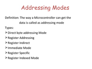
- 1. Addressing Modes Definition: The way a Microcontroller can get the data is called as addressing mode Types: Direct byte addressing Mode Register Addressing Register Indirect Immediate Mode Register Specific Register Indexed Mode
- 2. Addressing Modes Direct Mode – specify data by its 8-bit address Usually for RAM Mov a, 70h ; copy contents of RAM at 70h to a Mov R0,40h ; copy contents of RAM at 40h to a Mov 56h,a ; put contents of a at 56h to a Mov PSW,a ; put contents of a into PSW MOV R2,#5 ;Put 5 in R2 MOV R2,5 ;Put content of RAM at 5 in R2
- 3. Addressing Modes Register Addressing – either source or destination is one of CPU register MOV R0,A MOV A,R7 ADD A,R4 ADD A,R7 MOV DPTR,#25F5H MOV R5,DPL MOV R,DPH Note that MOV R4,R7 is incorrect
- 4. Addressing Modes Register Indirect (@) – the address of the source or destination is specified in registers Uses registers R0 or R1 for 8-bit address: mov @r0, #03 mov @r1, a mov @r1, 50 Uses DPTR register for 16-bit addresses: mov dptr, #1234 ; dptr 1234h movx a, @dptr ; a M[1234] Note that 1234 is an address in external memory
- 5. Addressing Modes Immediate Mode – Data is a part of an Instruction mov A, #0 ;put 0 in the accumulator ;A = 00000000 mov R4, #11h ;put 11hex in the R4 register ;R4 = 00010001 mov B, #11 ;put 11 decimal in b register ;B = 00001011 mov DPTR,#7521h ;put 7521 hex in DPTR ;DPTR = 0111010100100001
- 6. Addressing Modes Register Specific (@) – the source and destination registers both are same. Uses registers A or DPTR SWAP A SWAP DPTR
- 7. Addressing Modes Register Indexed Mode – source or destination address is the sum of the base address and the accumulator(Index) • Base address can be DPTR or PC – mov dptr, #4000h – mov a, #5 – movc a, @a + dptr ;a M[4005]
- 8. 8051- INSTRUCTION SET Data Copy or transfer instructions Data processing instructions Arithmetic instructions Logical instructions Program flow or Branching instructions JUMP CALL & RET Single Bit operation Instructions
- 9. Data Transfer Instructions • MOV dest, source dest source • Stack instructions PUSH byte ;increment stack pointer, ;move byte on stack POP byte ;move from stack to byte, ;decrement stack pointer • Exchange instructions XCH a, byte ;exchange accumulator and byte XCHD a, byte ;exchange low nibbles of ;accumulator and byte
- 10. MOV MOV dest, source dest source mov a,#0ffh mov p0,a mov R0, a mov a, R1 Movx a,@DPTR MovC a,@DPTR
- 11. Stack • Direct addressing mode must be used in Push and Pop mov sp, #0x40 ; Initialize SP Push 55 ; SP SP+1, ; M[41] M[55] pop b ; b M[55] push acc Push psw Push b
- 12. Exchange Instructions two way data transfer XCH a, 30h ; a M[30] XCH a, R0 ; a R0 XCH a, @R0 ; a M[R0] XCHD a, R0 ; exchange “digit” R0[7..4] R0[3..0]a[7..4] a[3..0] Only 4 bits exchanged
- 13. Data Processing Instructions Arithmetic Instructions Logic Instructions
- 14. Arithmetic Instructions • Add • Subtract • Increment • Decrement • Multiply • Divide
- 15. Arithmetic Instructions Mnemonic Description ADD A, byte add A to byte, put result in A ADDC A, byte add with carry SUBB A, byte subtract with borrow INC A increment A INC byte increment byte in memory INC DPTR increment data pointer DEC A decrement accumulator DEC byte decrement byte MUL AB multiply accumulator by b register DIV AB divide accumulator by b register
- 16. ADD Examples mov a, #3Fh add a, #D3h • What is the value of the C, AC, OV flags after the second instruction is executed? 0011 1111 1101 0011 0001 0010 C = 1 AC = 1 OV = 0
- 17. Logic Instructions Bitwise logic operations (AND, OR, XOR, NOT) Clear Rotate Swap
- 18. Bitwise Logic ANL AND ORL OR XRL XOR CPL Complement Examples: 00001111 10101100ANL 00001111 10101100ORL 00001111 10101100XRL 10101100CPL 00001100 10101111 10100011 01010011
- 19. CLR ( Set all bits to 0) CLR A CLR byte (direct mode) CLR Ri (register mode) CLR @Ri (register indirect mode)
- 20. Rotate • Rotate instructions operate only on a RL a Mov a,#0xF0 ; a 11110000 RR a ; a 11100001 RR a Mov a,#0xF0 ; a 11110000 RR a ; a 01111000
- 21. Rotate through Carry RRC a mov a, #0A9h; a A9 add a, #14h ; a BD (10111101), C0 rrc a ; a 01011110, C1 RLC a mov a, #3ch ; a 3ch(00111100) setb c ; c 1 rlc a ; a 01111001, C1 C C
- 22. Swap SWAP a mov a, #72h ; a 72h swap a ; a 27h
- 23. Program Flow Control • Unconditional jumps Program transfer is permanent • Conditional jumps Call and return Program transfer is temporary
- 24. Unconditional Jumps • SJMP <rel addr 8-bit > ; Short jump, relative address is 8-bit, so jump can be up to 127 locations forward, or 128 locations back. • AJMP <address 11> ; Absolute jump to anywhere within 2K block of program memory(07FF H) • LJMP <address 16> ; Long jump(64 k 0000-FFFF H)
- 25. Infinite Loops Start: mov C, p3.7 mov p1.6, C sjmp Start Microcontroller application programs are almost always infinite loops!
- 26. Conditional jumps Mnemonic Description JZ <rel addr> Jump if a = 0 JNZ <rel addr> Jump if a != 0 JC <rel addr> Jump if C = 1 JNC <rel addr> Jump if C != 1 JB <bit>, <rel addr> Jump if bit = 1 JNB <bit>,<rel addr> Jump if bit != 1 JBC <bir>, <rel addr> Jump if bit =1, &clear bit CJNE A, direct, <rel addr> Compare A and memory, jump if not equal
- 27. More Conditional Jumps Mnemonic Description CJNE A, #data <rel addr> Compare A and data, jump if not equal CJNE Rn, #data <rel addr> Compare Rn and data, jump if not equal CJNE @Rn, #data <rel addr> Compare Rn and memory, jump if not equal DJNZ Rn, <rel addr> Decrement Rn and then jump if not zero DJNZ direct, <rel addr> Decrement memory and then jump if not zero
- 28. Call and Return • Call is similar to a jump, but – Call pushes PC on stack before branching acall <address ll> ; stack PC ; PC address 11 bit lcall <address 16> ; stack PC ; PC address 16 bit
- 29. Return • Return is also similar to a jump, but – Return instruction pops PC from stack to get address to jump to – ret ; PC stack
- 30. Bit-Oriented Data Transfer • transfers between individual bits. • Carry flag (C) (bit 7 in the PSW) is used as a single-bit accumulator • RAM bits in addresses 20-2F are bit addressable mov C, P0.0 mov C, 67h mov C, 2ch.7
- 31. Bit-Oriented Data Transfer • CLR Bit Ex:- CLR C, CLR P1.2 • SETB Bit Ex:- SETB C, SET P1.2, SETB PSW.3 • CPL Bit CPL C • Single bit Logical Operation Instructions AND Operation: ANL C, PSW.2 OR Operation : ORL C , ACC.7
- 32. TIMER / COUNTER PROGRAMMING Indicate which mode and which timer are selected for each of the following. (a) MOV TMOD,#01H (b) MOV TMOD,#20H (c) MOV TMOD,#12H Solution: (a) TMOD = 00000001, mode 1 of timer 0 is selected. (b) TMOD = 00100000, mode 2 of timer 1 is selected. (c) TMOD = 00010010 mode 2 of timer 0, and mode 1 of timer 1 are selected. timer 1 timer 0 GATE C/T M1 M0 GATE C/T M1 M0 Timer 1 Timer 0 (MSB) (LSB)
- 33. TIMER PROGRAMMING Find the timer’s clock frequency and its period for various 8051- based systems, with the following crystal frequencies. (a) 12 MHz (b) 16 MHz (c) 11.0592 MHz Solution: (a) 1/12 × 12 MHz = 1 MHz and T = 1/1 MHz = 1 µs (b) 1/12 × 16 MHz = 1.333 MHz and T = 1/1.333 MHz = 0.75 µs (c) 1/12 × 11.0592 MHz = 921.6 KHz; T = 1/921.6 KHz = 1.085 µs XTAL oscillator ÷ 12
- 34. Mode 1 Programming XTAL oscillator ÷ 12 TR TH TL TF TF goes high when FFFF 0 overflow flag C/T = 0 like MC for 89C51 Start timer
- 35. Steps of Mode 1 1. Chose mode 1 timer 0 – MOV TMOD,#01H 2. Set the original value to TH0 and TL0.(FCFF H) – MOV TH0,#0FFH – MOV TL0,#0FCH 3. You had better to clear the flag to monitor: TF0=0. – CLR TF0 4. Start the timer. – SETB TR0
- 36. Steps of Mode 1 5.The 8051 starts to count up by incrementing the TH0-TL0. FFFCH,FFFDH,FFFEH,FFFFH,0000H FFFC FFFD FFFE FFFF 0000 TF0=0 TF0=0 TF0=0 TF0=0 TF0=1 TH0 TL0Start timer Stop timer TR0=1 TR0=0 Roll over
- 37. Steps of Mode 1 6. When TH0-TL0 rolls over from FFFFH to 0000, the 8051 set TF0=1. 7. Keep monitoring the timer flag (TF) to see if it is raised. – AGAIN: JNB TF0, AGAIN 8. Clear TR0 to stop the process. – CLR TR0 9. Clear the TF flag for the next round. – CLR TF0
- 38. Initial Count Values • The initial count value = FFFC. • The number of counts = FFFFH-FFFCH+1 = 4 – we add one to 3 because of the extra clock needed when it rolls over from FFFF to 0 and raises the TF flag. • The delay = 4 • If T=1.085 µs, then the delay = 4 X T 4.34 µs
- 39. Example MOV TMOD,#01 ;Timer 0,mode 1(16-bit) HERE: MOV TL0,#0F2H ;Timer value = FFF2H MOV TH0,#0FFH CPL P1.5 ACALL DELAY SJMP HERE DELAY: SETB TR0 ;start the timer 0 AGAIN:JNB TF0,AGAIN CLR TR0 ;stop timer 0 CLR TF0 ;clear timer 0 flag RET
- 40. SOLUTION In Example , calculate the amount of time delay in the DELAY subroutine generated by the timer. Assume that XTAL = 11.0592 MHz. Solution: The timer works with the internal system clock. frequency of internal system clock = 11.0592/12 = 921.6 KHz machine cycle = 1 /921.6 KHz = 1.085 µs (microsecond) The number of counts = FFFFH – FFF2H +1 = 14 (decimal). The delay = number of counts × 1.085 µs = 14 × 1.085 µs = 15.19 µs for half the clock. For the entire period of a clock, it is T = 2 × 15.19 µs = 30.38 µs as the time delay generated by the timer.
- 41. Largest Time Delay IN MODE 0 Solution: TH0=TL0=0000 means that the timer will count from 0000 to FFFF, and then roll over to raise the TF0 flag. As a result, it goes through a total of 65536 states. Therefore, we have delay = (65536 – 0) × 1.085 µs = 71.1065 ms.
- 42. Find Timer COUNT Values • Assume XTAL = 11.0592 MHz . • How to find the inter values needed for the TH, TL to produce exact delay of 20 ms? Step-1 -Divide the desired time delay by 1.085 µs. 20ms ÷ 1.085 µs = 18433 Step2-Perform 65536 –n, where n is the decimal value we got in Step 1. 65536-18433= 47103 = B7FFH – Convert the result of Step 2 to hex, where B7FF is the initial hex value to be loaded into the timer’s registers. – Set TH=B7H, TL=FFH
- 43. Example 2 Assuming XTAL = 11.0592 MHz, write a program to generate a square wave of 50 Hz frequency on pin P2.3. Solution: Look at the following steps. (a) The period of the square wave = 1 / 50 Hz = 20 ms. (b) The high or low portion of the square wave = 10 ms. (c) 10 ms / 1.085 µs = 9216 65536 – 9216 = 56320 in decimal = DC00H in hex. (d) TL1 = 00H and TH1 = DCH.
- 44. Mode 2 programming XTAL oscillator ÷ 12 TR TL TH TF TF goes high when FF 0 overflow flag C/T = 0 reload
- 45. Steps of Mode 2 1. Chose mode 2 timer 0 – MOV TMOD,#02H 2. Set the original value to TH0. – MOV TH0,#FCH 3. Clear the flag to TF0=0. – CLR TF0 4. Start the timer. – SETB TR0 – Note that the instruction SETB TR0 dose not load TH0 to TL0. So TL0 still is 00H.
- 46. Steps of Mode 2 (2/3) 5. The 8051 starts to count up by incrementing the TL0. – TL0= ..., FCH,FDH,FEH,FFH,FCH 00 01 FC FD FE TF0 = 0 TF0 = 0 TF0 = 0 TF0 = 0 TF0 = 0 TH0=FCH TL0=00H Start timer TR0=1 FF FC FD FE TF0 = 0 TF0 =0 TF0 = 0 TF0 = 0 TF0 = 0 Clear TF0 TF0=0 FF TL0=FCH auto reload TH0=FCH roll over auto reload: TL=-FCH immediately TF0 = 1 roll over ... 00H 00H
- 47. Steps of Mode 2 (3/3) 6. When TL0 rolls over from FFH to 00, the 8051 set TF0=1. Also, TL0 is reloaded automatically with the value kept by the TH0. – TL0= FCH, FDH, FEH, FFH, FCH(Now TF0=1) – The 8051 auto reload TL0=TH0=FCH. – Go to Step 6 (i.e., TL0 is incrementing continuously). •. Note that we must clear TF0 when TL0 rolls over. Thus, we can monitor TF0 in next process. •. Clear TR0 to stop the process. 00H
- 48. Example 9-14 (1/2) Assuming that XTAL = 11.0592 MHz, find (a) the frequency of the square wave generated on pin P1.0 in the following program (b) the smallest frequency achievable in this program, and the TH value to do that. MOV TMOD,#20H ;Timer 1,mode 2 MOV TH1,#5 ;not load TH1 again SETB TR1 ;start (no stop TR1=0) BACK:JNB TF1,BACK CPL P1.0 CLR TF1 ;clear timer flag 1 SJMP BACK ;mode 2 is auto-reload
- 49. Example 9-14 (2/2) Solution: (a) First notice that target address of SJMP. In mode 2 we do not need to reload TH since it is auto-reload. Half period = (FFH – 05 +1) × 1.085 µs = 272.33 µs Total period = 2 × 272.33 µs = 544.67 µs Frequency = 1.83597 kHz. (b) To get the smallest frequency, we need the largest period and that is achieved when TH1 = 00. Total period = 2 × 256 × 1.085 µs = 555.52 µs Frequency = 1.8kHz.
- 50. Counter programming • These timers can also be used as counters counting events happening outside the 8051 by setting C/T=1. • The counter counts up as pulses are fed from – T0: timer 0 input (Pin 14, P3.4) – T1: timer 1 input (Pin 15, P3.5) T0 to LCD P3.4 P1 8051 a switch TL0 TH0 Vcc Counter 0
- 51. Counter (2/2) • When the timer is used as a counter, it is a pulse outside of the 8051 that increments – TH0 & TL0 for counter 0. – TH1 & TL1 for counter 1. T1 to LCD P3.5 P1 8051 a switch TL1 TH1 Vcc Counter 1
- 52. Port 3 Pins Used For Timers 0 and 1 Pin Port Pin Function Description 14 P3.4 T0 Timer/Counter 0 external input 15 P3.5 T1 Timer/Counter 1 external input GATE C/T=1 M1 M0 GATE C/T=1 M1 M0 Timer 1 Timer 0 (MSB) (LSB)
- 53. Counter Mode 1 • 16-bit counter (TH0 and TL0) • TH0-TL0 is incremented when TR0 is set to 1 and an external pulse (in T0) occurs. • When the counter (TH0-TL0) reaches its maximum of FFFFH, it rolls over to 0000, and TF0 is raised. • Programmers should monitor TF0 continuously and stop the counter 0. • Programmers can set the initial value of TH0-TL0 and let TF0 as an indicator to show a special condition. (ex: 100 people have come).
- 54. Counter Mode 2 • 8-bit counter. – TL0 is incremented if TR0=1 and external pulse occurs. • Auto-reloading – TH0 is loaded into TL0 when TF0=1. – It allows only values of 00 to FFH to be loaded into TH0. – You need to clear TF0 after TL0 rolls over. • See Figure 9.6, 9.7 for logic view • See Examples 9-18, 9-19
- 55. Example Assuming that clock pulses are fed into pin T1, write a program for counter 1 in mode 2 to count the pulses and display the state of the TL1 count on P2. Solution: We use timer 1 as an event counter where it counts up as clock pulses are fed into pin3.5. P2 is connected to 8 LEDs and input T1 to pulse. T1 to LEDs P3.5 P2 8051
- 56. Example MOV TMOD,#01100000B ;mode 2, counter 1 MOV TH1,#0 SETB P3.5 ;make T1 input port AGAIN:SETB TR1 ;start BACK: MOV A,TL1 MOV P2,A ;display in P2 JNB TF1,BACK ;overflow CLR TR1 ;stop CLR TF1 ;make TF=0 SJMP AGAIN ;keep doing it Notice in the above program the role of the instruction “SETB P3.5”. Since ports are set up for output when the 8051 is powered up , we must make P3.5 an input port by making it high.
- 57. 8051 Serial Communication Programming TxD and RxD pins • In 8051, the data is received from or transmitted to – RxD: received data (Pin 10, P3.0) – TxD: transmitted data (Pin 11, P3.1)
- 58. Data Transfer Rate • How fast is the data transferred? • Methods to describe the speed: – Baud rate is defined as the number of signal changes per second. – The rate of data transfer is stated in Hz. – Date rate is defined as the number of bits transferred per second. – Each signal has several voltage levels. – The rate of data transfer is stated in bps (bits per second).
- 59. Standard Baud Rates 110 bps 150 300 600 1200 2400 4800 9600 (default) 19200 Various Baud Rates
- 60. 60 Baud Rate Comparison for SMOD = 0 and SMOD =1 XTAL oscillato r ÷ 12 ÷ 16 ÷ 32 Machine cycle freq. 921.6 kHz 57600 Hz 28800 Hz To timer 1 to set baud rate 11.0592 MHz SMOD = 1 SMOD = 0
- 61. Find Count Value in TH1 to generate Baud rate With XTAL = 11.0592 MHz, find the TH1 value needed to have the following baud rates. (a) 9600 (b) 2400 (c) 1200. Assume SMOD = 0 Solution: With XTAL = 11.0592 MHz, we have: The frequency of system clock = 11.0592 MHz / 12 = 921.6 kHz The frequency sent to timer 1 = 921.6 kHz/ 32 = 28,800 Hz (a) TH1 = FF – {Fosc /(12X32X9600)} TH1 = 256-{11.0952X10⁶ /(12X32X9600)} TH1 = 256-3 253(Decimal) FD H
- 62. 62 Baud Rate Comparison for SMOD = 0 and SMOD =1 TH1 (Decimal) (Hex) SMOD = 0 SMOD = 1 253 FD 9,600 19,200 250 FA 4,800 9,600 244 F4 2,400 4,800 232 E8 1,200 2,400 Note: XTAL = 11.0592 MHz. XTAL oscillato r ÷ 12 ÷ 16 ÷ 32 Machine cycle freq. 921.6 kHz 57600 Hz 28800 Hz To timer 1 to set baud rate 11.0592 MHz SMOD = 1 SMOD = 0
- 63. Transfer steps • The following sequence is the steps that the 8051 goes through in transmitting a character via TxD: 1. The byte character to be transmitted is written into the SBUF register. 2. It transfers the start bit. 3. The 8-bit character is transferred one bit at a time. 4. The stop bit is transferred. SBUF TxD bit by bit 8-bit char UARTTI
- 64. Transfer data Serially Example 1 Write a program for the 8051 to transfer letter “A” serially at 4800 baud, continuously. Use the timer 1 in mode 2. Assume SMOD = 0 Solution: MOV TMOD,#20H ;timer 1, mode 2 MOV TH1,#-6 ;4800 baud rate MOV SCON,#50H ;8-bit,1 stop,REN enabled SETB TR1 ;start timer 1 AGAIN: MOV SBUF,#”A” ;letter “A” to be transferred HERE: JNB TI,HERE ;wait for the last bit CLR TI ;clear TI for next char SJMP AGAIN ;keep sending A
- 65. Example 2 Write a program to transfer the message “YES” serially at 9600 baud, 8-bit data, 1 stop bit. Do this continuously. Solution: MOV TMOD,#20H ;timer 1, mode 2 MOV TH1,#-3 ;9600 baud MOV SCON,#50H SETB TR1 AGAIN:MOV A,#”Y” ;transfer “Y” ACALL TRANS MOV A,#”E” ;transfer “E” ACALL TRANS MOV A,#”S” ;transfer “S” ACALL TRANS SJMP AGAIN ;keep doing it
- 66. Example 2 ;serial data transfer subroutine TRANS:MOV SBUF,A ;load SBUF HERE: JNB TI,HERE ;wait for last bit to transfer CLR TI ;get ready for next byte RET
- 67. Receive Data Serially • The following sequence is the steps that the 8051 goes through in receiving a character via RxD: 1. 8051 receives the start bit indicating that the next bit is the first bit of the character to be received. 2. The 8-bit character is received one bit at a time. When the last bit is received, a byte is formed and placed in SBUF. SBUFRxD bit by bit 8-bit character UART RI
- 68. Example 1 Program the 8051 to receive bytes of data serially, and put them in P1. Set the baud rate at 4800, 8-bit data, and 1 stop bit. Solution: MOV TMOD,#20H ;timer1, mode 2 (auto reload) MOV TH1,#-6 ;4800 baud MOV SCON,#50H ;8-bit, 1 stop, REN enabled SETB TR1 ;start timer 1 HERE: JNB RI,HERE ;wait for char to come in MOV A,SBUF ;save incoming byte in A MOV P1,A ;send to port 1 CLR RI ;get ready to receive next byte SJMP HERE ;keep getting data
- 69. HOME WORK MOV A,PCON SETB ACC.7 MOV PCON,A ;SMOD=1, double baud rate MOV TMOD,#20H ;Timer 1, mode 2,auto reload MOV TH1,#-3 ;19200 baud rate MOV SCON,#50H ;8-bit data,1 stop bit, RI enabled SETB TR1 ;start Timer 1 MOV A,#”B” ;transfer letter B A_1:CLR TI ;make sure TI=0 MOV SBUF,A ;transfer it H_1:JNB TI H_1 ;check TI SJMP A_1 ;do again
- 70. SOLUTION Assuming that XTAL = 11.0592 MHz for the following program, state (a) what this program does, (b) compute the frequency used by timer 1 to set the baud rate, and (c) find the baud rate of the data transfer.Assume SMOD=1. Solution: (a) This program transfers ASCII letter B (01000010 binary) continuously. (b) and (c) With XTAL = 11.0592 MHz and SMOD = 1 11.0592 / 12 = 921.6 kHz machine cycle frequency. 921.6 /16 = 57,600 Hz frequency used by timer 1 to set the baud rate. 57,600 / 3 = 19,200, the baud rate.
- 71. INTERRUPT PROGRAMMING TIMER INTERRUPT PROGRAMMING • TIMER Interrupt occurred when Timer Flag (TFO or TF1) comes to set condition. • Overflow occurred at Roll-over of TIMER from FFFF to 0000 will set TFO or TF1 1 TF0 jumps to 0000 .... 000 B.... .... ISR of timer0 Timer 0 Interrupt Vector: 000BH 1 TF1 jumps to 0000 .... .... 001 B.... ISR of timer1 Timer 1 Interrupt Vector: 001BH
- 72. Example 1 Write a program that continuously gets 8-bits data from P0 and sends it to P1 while simultaneously creating a square wave of 200 µs period on pin P2.1. Use timer 0 to create the square wave. Assume that XTAL = 11.0592 MHz. Solution: We will use timer 0 in mode 2 (auto reload). TH0 = 100 µs /1.085 µs = 92 for half clock. We must avoid using memory space allocated to interrupt vector table. Therefore, we place the main memory in 0030H 1 TF0 jumps to 0000 .... 000 B.... .... 0030 .... ISR of timer0 main program interrupt vector table 100 µs 100 µs200 µs P2.1
- 73. Example 1 ORG 0000H LJMP MAIN ;by-pass interrupt vector table ORG 000BH ;Timer 0 interrupt vector table CPL P2.1 ;toggle P2.1 pin RETI ;return from ISR The main program for initialization ORG 0030H ;after vector table space MIAN: MOV TMOD,#02H ;Timer 0,mode 2(auto reload) MOV P0,0FFH ;make P0 an input port MOV TH0,#0A4H ;TH0=A4H for -92 MOV IE,#82H ;IE=100000010(bin) enable Timer 0 SETB TR0 ;Start Timer 0 BACK: MOV A,P0 ;get data from P0 and put it to P1 MOV P1,A ;loop unless interrupted by TF0 SJMP BACK END
- 74. Example 2 Create a square wave that has a high portion of 1085 µs and a low portion of 15 µs. Assume XTAL = 1.0592 MHz. Use timer 1. Solution: we need to use mode 1 of timer 1. 1085 µs /1.085 µs = ? Count value for ON time 15 µs /1.085 µs = ? Count value for OFF time 1 TF1 jumps to 0000 .... 001 B.... .... 0030 .... ISR of timer1 main program interrupt vector table 1085 µs 15 µs P2.1
- 75. Example 2 ORG 0000H ;by-pass interrupt vector table LJMP MAIN ORG 001BH ;timer 1 interrupt vector table LJMP ISR_T1 ;jump to ISR ;The main program for initialization ORG 0030H ;after vector table MAIN: MOV TMOD,#10H ;timer 1, mode 1 MOV P0,#0FFH ;make P0 an input port MOV TL1,#018H ;TL1=18 the low byte of -1000 MOV TH1,#0FCH ;TH1-FC the high byte of -1000 MOV IE,#88H ;IE=1001000 enable timer 1. SETB TR1 ;start timer 1
- 76. Example 2 ISR_T1:CLR TR1 ;stop Timer 1 CLR P2.1 ;P2.1=0, start of low portion MOV TL1,#18H ;load T1 low byte value (2 MC) MOV TH1,#0FCH ;load T1 high byte value (2 MC) SETB TR1 ;starts timer 1 (1 MC) SETB P2.1 ;P2.1=1, back to high (1 MC) RETI ;return to main END
- 77. Example -3 Write a program to generate a square wave of 50 Hz frequency on pin P1.2. Assume that XTAL=11.0592 MHz. Find the count value to be loaded in TIMER 0. Solution: (a) The period of the square wave = 1 / 50 Hz = 20 ms. (b) The half square wave = 10 ms = (10 ms /1.085 µs) = 9216 65536 – 9216 = 56320 in decimal = DC00H in hex. ORG 0 LJMP MAIN ORG 000BH CPL P1.2 RETI 50% 50% 20ms P1.2
- 78. Example -3 ;--main program for initialization ORG 30H MAIN: MOV TMOD,#00000001B ;timer 0, mode 1 MOV TL0,#00 MOV TH0,#0DCH MOV IE,#10000010B ;enable timer 0 interrupt SETB TR0 HERE: SJMP HERE END P1.2 8051 TL0 TH0 50 MHz square wave
- 79. Programming External Hardware Interrupts • The 8051 has two external hardware interrupts: – EX0: INT0, Pin 12 (P3.2) – EX1: INT1, Pin 13 (P3.3) • They are enabled and disabled using the IE register. – EX0 by IE.0 – EX1 by IE.1 TF1 TR1 TF0 TR0 IE1 IT1 IE0 IT0 Timer 1 Timer0 for Interrupt (MSB) (LSB)
- 80. Figure 4-1. 8051 Pin Diagram PDIP/Cerdip 1 2 3 4 5 6 7 8 9 10 11 12 13 14 15 16 17 18 19 20 40 39 38 37 36 35 34 33 32 31 30 29 28 27 26 25 24 23 22 21 P1.0 P1.1 P1.2 P1.3 P1.4 P1.5 P1.6 P1.7 RST (RXD)P3.0 (TXD)P3.1 (T0)P3.4 (T1)P3.5 XTAL2 XTAL1 GND (INT0)P3.2 (INT1)P3.3 (RD)P3.7 (WR)P3.6 Vcc P0.0(AD0 )P0.1(AD1) P0.2(AD2 )P0.3(AD3) P0.4(AD4) P0.5(AD5) P0.6(AD6) P0.7(AD7) EA/VPP ALE/PROG PSEN P2.7(A15) P2.6(A14) P2.5(A13) P2.4(A12) P2.3(A11) P2.2(A10) P2.1(A9) P2.0(A8) 8051 (8031) external hardware interrupt
- 81. Activation of INT0 IE0 (TCON.1) INT0 (Pin 3.2) Interrupt Service Table with addr. 0003H Edge-triggered level-triggered IT 0 =0 IT 0 =1 INT0 INT0 IE0=1 IE0=0
- 82. Example 1 Assume that the INT1 pin is connected to a switch that is normally high. Whenever it goes low, it should turn on an LED. The LED is connected to P1.3 and is normally off. When it is turned on, it should stay on for a fraction of a second. As long as the switch is pressed low, the LED should stay on. Solution: Pressing the switch will cause the LED to be turned on. If it is kept activated, the LED stays on. To LED 8051 P1.3 INT1 Vcc
- 83. Example 1 ORG 0000H LJMP MAIN ORG 0013H SETB P1.3 MOV R3,#255 BACK: DJNZ R3,BACK CLR P1.3 RETI main program for initialization ORG 0030H MAIN: MOV IE,#10000100B ;enable INT1 HERE: SJMP HERE ;stay here until get interrupt END
- 84. Example 2 Assuming that pin 3.3 (INT1) is connected to a pulse generator, write a program in which the falling edge of the pulse will send a high to P1.3 which is connected to an LED (or buzzer). In other words, the LED is turned on and off at the same rate as the pulses are applied to the INT1 pin. This is an edge-triggered version of Example 11-5. But in this example, to turn on the LED again, the INT1 pulse must be brought back high and then forced low to create a falling edge to activate the interrupt. INT1 to LED P3.3 P1.3 8051 a switch pulse generator
- 85. Example 2 ORG 0000H LJMP MAIN ORG 0013H SETB P1.3 MOV R3,#255 BACK: DJNZ R3,HERE ;keep the buzzer on for a while CLR P1.3 RETI MAIN program for initialization ORG 0030H MAIN: SETB TCON.2 ;make INT1 edge-trigger interrupt MOV IE,#10000100B ;enable External INT 1 HERE: SJMP HERE END
- 86. Programming the Serial Communication Interrupt Write a program in which the 8051 reads data from P1 and writes it to P2 continuously while giving a copy of it to the serial COM port to be transferred serially. Assume that XTAL=11.0592. Set the baud rate at 9600. Solution: ORG 0000 LJMP MAIN ORG 23H LJMP SERIAL ;jump to serial interrupt ISR ORG 0030H MAIN: MOV P1,#OFFH ;make P1 an input port MOV TMOD,#20H ;timer 1,mode 2 (auto reload) MOV TH1,#OFDH ;9600 baud rate MOV SCON,#50H ;8-bit, 1 stop, REN enabled MOV IE,#10010000B ;enable serial interrupt SETB TR1 ;start timer 1
- 87. Example 1 ;------ stay in loop indefinitely ------ BACK: MOV A,P1 MOV SBUF,A ;A has a copy of data MOV P2,A SJMP BACK ;------ Serial communication ISR ------ ORG 100H SERIAL: JB TI,TRANS ;jump if TI is high RETI TRANS: MOV SBUF,A ;transmit the copy of P1 CLR TI ;clear TI RETI END
Hinweis der Redaktion
- &lt;number&gt; 要特別注意, JNB 需要 2 個 MCs. 所以每執行一次 JNB, TH0-TL0 會加 2. 在執行完 AGAIN 迴圈, JNB 發現 TF0 != 0, 離開 AGAIN, 將要執行 CLR TR0, 此時 TH0-TL0 = 0002.
- &lt;number&gt; Ask whether the answer 30.38 is precise enough or not. 是一點點不準或很不準?
- &lt;number&gt; Ex: 想要產生 200 ms 的 time delay. 200,000÷1.085=184332. 65536-184332=47203=B863H, TH=B8H, TL=63H
- &lt;number&gt; 在 timer/counter mode 2, 只有當 TL 從 FFH rolls over 成00H 時, TH 會被載入 TL. 對於 timer 第一次啟動時, 因為沒有任何 roll over 的動作, 所以 TL 的值為 00H (if no initial value for TL), TL 會從 00H 開始往上數. 直到第一次 TL rolls over (FFH -&gt; 00H), TL 才會被設成 TH, 以後的運作才會按照 TH 的設定來產生 time delay.