➥🔝 7737669865 🔝▻ narsinghpur Call-girls in Women Seeking Men 🔝narsinghpur🔝 ...
Aem Lect19
1. 삼성전기, 초소형 복합기능
휴대폰부품 FEM 국내 첫 개발
게재: 2001년 05월 24일 (전자엔지니어)
삼성전기가 유럽향 듀얼 휴대폰에 사용되는 핵심부품 FEM(Front End Module)을
개발했다. 가로(8.4mm) X 세로(5.0mm) X 높이(1.9mm)의 크기로 7개의 낱개 부품을 사용할
때보다 부피를 80퍼센트 줄여주는 FEM은 휴대폰에 사용되어 송신과 수신신호를 분리시켜
주며, 여러 주파수 중 필요한 주파수만을 선택해 통과시켜주는 역할을 담당하는 다기능
부품이다. 이 부품은 기존 부품보다 가격면에서 25퍼센트 저렴하다.
삼성전기 측은 이 제품의 개발을 위해 1mm 높이의 LTCC(저온 소성 세라믹)기판에 적층
설계 기법을 사용하여 13층의 회로를 구현했으며, SAW 필터를 내장시켜 고주파 회로에서
저항을 최소화하는데 성공했다고 전했다. 일본의 히타치 외에 다른 업체들이 모두 개발 중에
있는 FEM은 히타치 제품에 비해 크기가 작아 큰 호응을 얻을 수 있을 것으로 기대되고 있다.
올해 세계 휴대폰 시장의 예상 규모가 5억3천만 대이고 그 중 60퍼센트가 유럽향
휴대폰이며, 그 대부분이 듀얼폰임을 감안할 때 FEM의 시장규모는 4억 달러 이상이 될 것으로
예상된다. 삼성전기 FEM의 본격 양산은 올 4사분기에 시작되며, 국내에서 최초 생산되지만
중국 시장 공략을 위해 텐진 공장에서 대량 생산을 할 계획이다.
삼성전기는 연간 1천만 대 이상의 유럽향 휴대폰을 생산하는 국내 휴대폰 업체들에 FEM을
공급해 1천만불 이상의 수입대체 효과를 거둘 것이며, 앞으로 플립칩 SAW 필터를 적용한 6.5 X
5.2 X 1.8mm의 초소형 제품을 개발, US PCD 대역까지 커버하는 트리플모드 복합제품도
개발할 것이라고 밝혔다.
Advanced Electronic Ceramics I (2004)
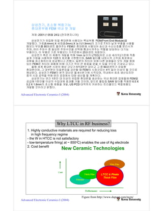
Why LTCC in RF business?
1. Highly conductive materials are required for reducing loss
in high frequency regime
- the W in HTCC is not satisfactory
- low-temperature firing( at ~ 850oC) enables the use of Ag electrode
2. Cost benefit
Figure from http://www.dupont.com/mcm/
Advanced Electronic Ceramics I (2004)
2. What is LTCC?
♦ High density glass/ceramic multilayer technology
♦ Technology used to create passive components such as
capacitors, resistors & inductors
♦ Use with photo patterned materials gives high
performance
♦ Allows direct attach of silicon and GaAs integrated
circuits
♦ Parallel processed technique - all layers produced
separately and co-fired in single process
♦ Ag & Au based conductors
♦ Buried and surface resistors, capacitors and inductors
♦ Low loss tape allows integration of filters, couplers etc.
From http://www.dupont.com/mcm/
Advanced Electronic Ceramics I (2004)
Messages from LTCC
♦ Cost (simple lamination and sintering)
♦ Size (Integration)
♦ Performance
♦ Time To Market
♦ Design Flexibility (parallel process
technique)
♦ Modularity of the passive components
From http://www.dupont.com/mcm/
Advanced Electronic Ceramics I (2004)
3. Thin film and LTCC
Thin film LTCC
Wiring density Very high high
Size Very small small
Process serial parallel
Cost high-cost cost-effective
(Chemical etching…) (screen printing & Sintering)
Time to market Long Short
1 week prototypes;
2 weeks production
Production scale Mass production Not only large but also
Small-scale production
Design flexibility Moderate Very good
From http://www.dupont.com/mcm/nextgen-handsets/handsets18.html
Advanced Electronic Ceramics I (2004)
LTCC: technology trends in RF
Advanced Electronic Ceramics I (2004)
4. Thermal via
For heat release
thermal conductivity
2-6 W/moK for LTCC
15-240 W/moK for HTCC
Thermal conductivity
- Alumina 100 times FR4
- LTCC 20 times FR4
- Thermal vias can be included
- LTCC allows heat pipe approach
From http://www.dupont.com/mcm/nextgen-handsets/handsets18.html
Advanced Electronic Ceramics I (2004)
LTCC materials
1. Borosilicate glass + Al2O3 (or mullite, cordierite)
: Al2O3 : 20-80%, B2O3, SiO2:10-70%
: the borosilicate component was added to the basic HTCC(Al2O3)
composition in order to decrease the sintering temperature
2. The role of Al2O3 (or mullite, cordierite)
- increase dielectric constant
- increase strength of LTCC
3. The decrease in dielectric constant can be attained by increasing
glass content
4. Other additives : K2O, Na2O, CuO, Fe2O3, Bi2O3, TiO2
Materials Issues
1. Increase in mechanical strength for soldering and post heat-treatment
2. The development of the composition with a low dielectric constant
for the high-frequency application
Private communication with Dr. Jae-Hwan Park in KIST
Advanced Electronic Ceramics I (2004)
5. LTCC materials: electrode, R,and C
Electrode
1. Typical material : Ag or Cu
1. Chemical compatibility
2. No interdiffusion between the electrode and LTCC substrate
3. No delamination due to the shrinkage mismatch and dewetting
Internal capacitor
1. BaTiO3 + SiO2, PbO, B2O3, Na2O, K2O, Al2O3
2. Match the sintering temperature for co-firing with LTCC
3. PMN, PFN-PFW can be used
Internal resistor
1. RuO2, Pb-pyrochlore, Bi-pyrochlore
Private communication with Dr. Jae-Hwan Park in KIST
Advanced Electronic Ceramics I (2004)
Typical LTCC process
Slit and Blank
Pre-condition
Layer 1 Layer 2 Layer 3 Layer 4
Form Vias Form Vias Form Vias Form Vias
Fill Vias Fill Vias Fill Vias Fill Vias
Conductor 1 Conductor 2 Conductor 3
Collate/Laminate
Burnout/Co-fire
Surface Layer Personalization
Singulation
Advanced Electronic Ceramics I (2004)
6. Typical LTCC process
1. Precondition : make optimum condition for processing
- heat treatment at 120oC for 20-30 min
- storage in nitrogen atmosphere for 24h
2. Blanking : punching for the sheet alignment using punch or lasor
3. Via fill : screen printing or extrusion
4. Printing conductor
5. Drying at 120oC for several minutes
6. Lamination at ~70oC
Advanced Electronic Ceramics I (2004)
LTCC: Example
Low temperature sintering : ~ 850oC
Employ the Ag electrode
http://www.murata.com/murata/murata.nsf/pages/multilayer/
Advanced Electronic Ceramics I (2004)
7. Typical LTCC process
♦ mil: milli inch = 0.001 inch
Via
Catch Pad
♦ Vias on the same layer
At least 3d for RF isolation
d: via diameter
Advanced Electronic Ceramics I (2004)
Typical LTCC process
Exposed Vias : maximum 22 layers
Buried Vias: Maximum 12 layers
Stagger
Advanced Electronic Ceramics I (2004)
8. Typical LTCC process
Minimum via-to-via spacing
Within the Between tape Via to edge
same tape layer
layer
http://www.vtt.fi/ele/research/ope/pdf_files/lcdes.pdf
Advanced Electronic Ceramics I (2004)
Typical LTCC process
1. Minimum conductor line
width(A) : 200 µm
2. Maximum conductor line
width : 1.5 mm
3. Minimum conductor
spacing(B) : 200 µm
4. Minimum conductor line
spacing(C) : 275 µm
4. The minimum conductor line clearance to the substrate edge(D):
125 µm
5. Minimum SMD pad spacing to a via pad (F) : 200 µm
6. Minimum SMD pad spacing to a conductor line (F) : 200 µm
7. Minimum SMD pad spacing to substrate edge (G) : 500 µm
http://www.vtt.fi/ele/research/ope/pdf_files/lcdes.pdf
Advanced Electronic Ceramics I (2004)
9. Layer Naming Scheme
http://www.vtt.fi/ele/research/ope/pdf_files/lcdes.pdf
Advanced Electronic Ceramics I (2004)
Via filling machine
Fill Small Vias In Green Ceramic Tape And Fired
Substrates With Pressure Injection
The VF-1000’s patented process is capable of filling vias as
small as 2 mils (50 mm) in ceramic tape, fired substrates
and various other microelectronics materials up to 8quot;
(203mm) square in size. Unlike screen printing, the VF-
1000 does not use vacuum to assist in the filling process,
minimizing the chance of a partial fill that can occur when
attempting to fill very small vias. Also unlike screen printing,
via ink in the VF-1000 is not continually exposed to air
which prevents the evaporation of solvents in the ink and
maintains a constant viscosity from the first part to the last.
In the VF-1000 the via fill ink is contained in a bladder-like
reservoir. When air pressure is applied to the bladder it
VF-1000 INJECTION
extrudes the ink through a stencil mask directly into the vias
VIA FILL SYSTEM
of the part you are filling. The mask is registered to the part
using the same tooling pins that are positioning the part on
- Fill Small Via Hole Completely
the vacuum stage. The ink forced into the vias naturally
- Air Pressure Fills All Holes Uniformly
displaces any trapped air and fills all the vias in the part
- The Via Fill Ink is Not Exposed to Air
simultaneously.
- Ability to Fill Fired Substrates
http://www.ptchips.com/
Advanced Electronic Ceramics I (2004)
10. Typical LTCC process
1. Surface resistor
- as fired tolerance : ± 30% in resistance
- laser trimmed tolerance: ± 1% in resistance
- trimmed resistor should be designed to fire
to 75 % of its nominal value for the later trimming into larger R
ex) considering the ± 30% fluctuation in resistance requires the
75 ohm in order to produce the 100 ± 1 ohm
75 X 0.70 = 52.5 ohm, 75 X 1.3 = 97.5 ohm
if the resistor is within ± 30% of fluctuation in resistance, 75% will do.
2. Buried resistor
- tolerance : ± 30% in resistance
- trimming is not available
Advanced Electronic Ceramics I (2004)
LTCC process
Stack
Blank
and
and
Tack
Frame
Module
High
Speed Firing
Punch
Screen
Final
Printing
Product
http://www.national.com/appinfo/ltcc/0,2583,367,00.html
Advanced Electronic Ceramics I (2004)
11. LTCC example: Bluetooth
What is Bluetooth? New communication standard for wireless connectivity.
Why the name Bluetooth? Bluetooth was named after 10th Century Danish King
Harold Bluetooth. King Harold was credited with uniting the provinces of
Denmark under a single crown. Bluetooth technology is suppose to unite all
different digital devices under a single standard of connection.
Advanced Electronic Ceramics I (2004)
Advantages of Thick Film and Green Tape in Automotive parts
- Proven Reliability
- High Circuit Density
- Integral Components
- Resistors & Functional Trimming
- Direct Chip Attach
- High Operating Temperature
- TCE Match to Si & GaAs
- Thermal Performance
- Mixed Analog, Digital, RF
- Integral Hermetic Packaging
- High Frequency properties
- Halogen free
- Compatibility with Pb-free solders
- Functional integration
From http://www.dupont.com/mcm/nextgen-handsets/handsets18.html
Advanced Electronic Ceramics I (2004)