SlideShare ist ein Scribd-Unternehmen logo
1 von 15
Downloaden Sie, um offline zu lesen
First Order Active RC Sections
Problem 1:
For the first order all pass filter (1st
APF = phase equalizer) shown below:
(i) Show that first order LPF can be obtained as: 1st
LPF = 1 - 1st
APF
(ii) Show that first order HPF can be obtained as: 1st
HPF = 1+1st
APF
(iii) Show that Band reject filter (BRF) can be obtained as: BRF = 1 + two
cascaded sections of 1st
APF
(iv) Show that Band pass filter (BPF) can be obtained as: BPF = 1 - two cascaded
sections of 1st
APF.
(v) Verify (i)-(iv) using Spice simulation.
First Order Active RC Sections
Problem 1:
For the first order all pass filter (1st
APF) shown below:
(i) Show that first order LPF can be obtained as: 1st
LPF = 1 - 1st
APF
Solution:
The transfer function of 1st
APF is given by
𝑇(𝑆) =
𝑉𝑜𝑢𝑡
𝑉𝑖𝑛
=
𝑆𝐶 − 𝐺 𝐺
𝑆𝐶 + 𝐺 𝐺
=
𝑆 −
1
𝑅 𝐺 𝐶
𝑆 +
1
𝑅 𝐺 𝐶
= −
1 − 𝑆𝐶𝑅 𝐺
1 + 𝑆𝐶𝑅 𝐺
Using subtractor based on op-amp where two inputs of the subtractor circuit are
the input voltage and the output of the 1st
APF. The output of the subtractor is
𝑉𝑜1
𝑉𝑖𝑛
= 1 − (−
1 − 𝑆𝐶𝑅 𝐺
1 + 𝑆𝐶𝑅 𝐺
) = (
1 + 𝑆𝐶𝑅 𝐺 + 1 − 𝑆𝐶𝑅 𝐺
1 + 𝑆𝐶𝑅 𝐺
)
𝑉𝑜1
𝑉𝑖𝑛
= (
2
1 + 𝑆𝐶𝑅 𝐺
)
It is 1st
order LPF. By using C = 0.1µF and RG = R = RF = 41.42kΩ:
The Dc gain is Dc gain = 20 log(2) = 6dB
the cut-off frequency is 𝜔 𝑜 =
1
𝐶𝑅 𝐺
= 241.42rad/ sec = 2𝜋 (38.4Hz)
(ii) Show that first order LPF can be obtained as: 1st
HPF = 1 +1st
APF
Solution:
The transfer function of 1st
APF is given by
𝑇(𝑆) =
𝑉𝑜𝑢𝑡
𝑉𝑖𝑛
= −
1 − 𝑆𝐶𝑅 𝐺
1 + 𝑆𝐶𝑅 𝐺
Using adder based on op-amp circuit where the two inputs of the adder circuit are
the input voltage and the output of the 1st
APF. The output of the adder is
−
𝑉𝑜1
𝑉𝑖𝑛
= 1 + (−
1 − 𝑆𝐶𝑅 𝐺
1 + 𝑆𝐶𝑅 𝐺
) = (
1 + 𝑆𝐶𝑅 𝐺 − 1 + 𝑆𝐶𝑅 𝐺
1 + 𝑆𝐶𝑅 𝐺
)
−
𝑉𝑜1
𝑉𝑖𝑛
= (
2𝑆𝐶𝑅 𝐺
1 + 𝑆𝐶𝑅 𝐺
)
It is 1st
HPF. By using C = 0.1µF and RG = R = RF = 41.42kΩ:
The Dc gain at 𝑇(𝑗𝜔 = ∞) is
Dc gain = 20 log(2) = 6dB
the cut-off frequency is
𝜔 𝑜 =
1
𝐶𝑅 𝐺
= 241.42rad/sec = 2π (38.4Hz)
(iii) Show that Band reject filter (BRF) can be obtained as: BRF = 1 + two
cascaded sections of 1st
APF (BRF = 1 + 2nd
APF)
Solution:
The transfer function of two cascaded section of 1st
APF is given by
𝑇(𝑆) = (−
1 − 𝑆𝐶𝑅 𝐺
1 + 𝑆𝐶𝑅 𝐺
) × (−
1 − 𝑆𝐶𝑅 𝐺
1 + 𝑆𝐶𝑅 𝐺
)
𝑇(𝑆) =
1 − 2𝑆𝐶𝑅 𝐺 + (𝑆𝐶𝑅 𝐺)2
1 + 2𝑆𝐶𝑅 𝐺 + (𝑆𝐶𝑅 𝐺)2
It is a 2nd
order APF.
𝜔𝑧 = 𝜔 𝑝 =
1
𝐶𝑅 𝐺
= 241.42 rad/sec = 2π (38.4Hz)
Using adder based on op-amp circuit where the two inputs of the adder circuit are
the input voltage and the output of the 2st
order APF. The output of the adder is
−
𝑉𝑜1
𝑉𝑖𝑛
= 1 + (
1 − 2𝑆𝐶𝑅 𝐺 + (𝑆𝐶𝑅 𝐺)2
1 + 2𝑆𝐶𝑅 𝐺 + (𝑆𝐶𝑅 𝐺)2
)
−
𝑉𝑜1
𝑉𝑖𝑛
=
1 + 2𝑆𝐶𝑅 𝐺 + (𝑆𝐶𝑅 𝐺)2
+ 1 − 2𝑆𝐶𝑅 𝐺 + (𝑆𝐶𝑅 𝐺)2
1 + 2𝑆𝐶𝑅 𝐺 + (𝑆𝐶𝑅 𝐺)2
−
𝑉𝑜1
𝑉𝑖𝑛
= 2
1 + (𝑆𝐶𝑅 𝐺)2
1 + 2𝑆𝐶𝑅 𝐺 + (𝑆𝐶𝑅 𝐺)2
It is 2nd
order notch filter. By using C = 0.1µF and RG = R = RF = 41.42kΩ:
In the two passbands ( ω → 0 and ω → ∞ ) the gain is
Dc gain = 20 log(2) = 6dB
while the notch frequency is
𝜔 𝑜 =
1
𝐶𝑅 𝐺
= 241.42rad/ sec = 2𝜋 (38.4Hz)
The pole quality factor Q is obtained as
𝜔 𝑜
𝑄
=
2
𝐶𝑅 𝐺
𝑄 =
𝜔 𝑜
2/𝐶𝑅 𝐺
= 0.5
𝑄 =
𝜔 𝑜
𝐵𝑊
= 0.5
𝐵𝑊 = (𝜔2 − 𝜔1) =
𝜔 𝑜
𝑄
= 482.84 rad/ sec = 2𝜋 (76.89Hz)
𝐵𝑊 = (𝜔2 − 𝜔1) =
𝜔 𝑜
𝑄
= 482.84 rad/sec
𝜔 𝑜 = √ 𝜔1 𝜔2 = 241.42 rad/sec
𝜔2 = 𝜔1 + 𝐵𝑊 = 𝜔1 + 482.84
𝜔2 =
𝜔 𝑜
2
𝜔1
=
(241.42)2
𝜔1
By substituting 𝜔2
𝜔1 + 482.84 =
(241.42)2
𝜔1
𝜔1
2
+ 482.84𝜔1 − (241.42)2
= 0
Either 𝜔1 = 100.123 rad/sec or 𝜔1 = −582.123 rad/sec (ignore)
∴ 𝜔1 = 100.123 rad/ sec = 2𝜋 (16Hz) → The lower cut-off frequency
𝜔2 = 𝜔1 + 𝐵𝑊 = 100.123 + 482.84 = 582.963 rad/ sec = 2𝜋 (93Hz)
𝜔2→ the higher cut-off frequency.
The depth of the notch in dB can be found as
|−
𝑉𝑜1
𝑉𝑖𝑛
| = |2|
|1 + (𝑗𝜔𝐶𝑅 𝐺)2|
|1 + 2𝑗𝜔𝐶𝑅 𝐺 + (𝑗𝜔𝐶𝑅 𝐺)2|
|−
𝑉𝑜1
𝑉𝑖𝑛
| = |2|
√(1 + −𝜔2 𝐶2 𝑅 𝐺
2
)
2
√(1 − 𝜔2 𝐶2 𝑅 𝐺
2
)
2
+ (2𝜔𝐶𝑅 𝐺)2
At notch frequency
𝜔 = 𝜔 𝑜 =
1
𝐶𝑅 𝐺
|−
𝑉𝑜1
𝑉𝑖𝑛
| = |2|
√(1 + −𝜔2 𝐶2 𝑅 𝐺
2
)
2
√(1 − 𝜔 𝑜
2 𝐶2 𝑅 𝐺
2
)
2
+ (2𝜔 𝑜 𝐶𝑅 𝐺)2
= 0
But practically we need to assume that there exists mismatch between simulated
cut-off frequency ωo,sim and calculated one 1/CRG due to their tolerances
(inaccurate component values) and may include PVT mismatches (the assumed
error value between calculated ωo and simulated ωo is about 1.1%):
𝑒𝑟𝑟𝑜𝑟 =
(𝜔 𝑜,𝑐𝑎𝑙 − 𝜔 𝑜,𝑠𝑖𝑚)
𝜔 𝑜,𝑐𝑎𝑙
× 100%
1.1% =
(241.42 − 𝜔 𝑜,𝑠𝑖𝑚)
241.42
× 100%
𝜔 𝑜,𝑠𝑖𝑚 = 238.75rad/sec
Now, the depth of the notch is
|−
𝑉𝑜1
𝑉𝑖𝑛
| = 2
√(1 − (238.75 × 0.004142)2)2
√(1 − (238.75 × 0.004142)2)2 + (2 × 238.75 × 0.004142)2
|−
𝑉𝑜1
𝑉𝑖𝑛
| = 2
0.02207
√(0.02207)2 + (1.9778)2
|−
𝑉𝑜1
𝑉𝑖𝑛
| = 2
0.02207
1.9779
= 0.02232
The notch depth in dB is
20log |−
Vo1
Vin
| = 20 log(0.02232) = −33dB
The notch rejection (the notch attenuation) is around 33dB.
If we use ω = ωo = 241.42rad/sec (approximated calculated value), then
|−
𝑉𝑜1
𝑉𝑖𝑛
| = 2
√(1 − (241.42 × 0.004142)2)2
√(1 − (241.42 × 0.004142)2)2 + (2 × 241.42 × 0.004142)2
|−
𝑉𝑜1
𝑉𝑖𝑛
| = 2
0.000076719
√(1 − 0.9999)2 + (1.9999)2
= 7.6719 × 10⁻⁵
The notch depth in dB is
20log |−
Vo1
Vin
| = 20 log(7.6719 × 10⁻⁵) = −82dB
The gain at the lower cut-off frequency ω1 is
|−
𝑉𝑜1
𝑉𝑖𝑛
| = 2
√(1 − (100.123 × 0.004142)2)2
√(1 − (100.123 × 0.004142)2)2 + (2 × 100.123 × 0.004142)2
|−
𝑉𝑜1
𝑉𝑖𝑛
| = 2
0.8280
√(0.8280)2 + (0.8294)2
= 1.413 𝑉/𝑉
The gain at the higher cut-off frequency ω2 is
|−
𝑉𝑜1
𝑉𝑖𝑛
| = 2
√(1 − (583.123 × 0.004142)2)2
√(1 − (583.123 × 0.004142)2)2 + (2 × 583.123 × 0.004142)2
|−
𝑉𝑜1
𝑉𝑖𝑛
| = 2
4.834
√(4.834)2 + (4.831)2
= 1.415 𝑉/𝑉
The gain in dB at both frequency is 3dB.
(iv) Show that Band pass filter (BPF) can be obtained as: BPF = 1 - two cascaded
sections of 1st
APF (BBF = 1 - 2nd
APF)
Solution:
The transfer function of two cascaded section of 1st
APF is given by
𝑇(𝑆) =
1 − 2𝑆𝐶𝑅 𝐺 + (𝑆𝐶𝑅 𝐺)2
1 + 2𝑆𝐶𝑅 𝐺 + (𝑆𝐶𝑅 𝐺)2
It is a 2nd
order APF.
𝜔𝑧 = 𝜔 𝑝 =
1
𝐶𝑅 𝐺
= 241.42 rad/sec = 2π (38.4Hz)
Using subtractor based on op-amp circuit where the two inputs of the subtractor
circuit are the input voltage and the output of the 2st
order APF. The output of the
subtractor is
𝑉𝑜1
𝑉𝑖𝑛
= 1 − (
1 − 2𝑆𝐶𝑅 𝐺 + (𝑆𝐶𝑅 𝐺)2
1 + 2𝑆𝐶𝑅 𝐺 + (𝑆𝐶𝑅 𝐺)2
)
𝑉𝑜1
𝑉𝑖𝑛
=
1 + 2𝑆𝐶𝑅 𝐺 + (𝑆𝐶𝑅 𝐺)2
− 1 + 2𝑆𝐶𝑅 𝐺 − (𝑆𝐶𝑅 𝐺)2
1 + 2𝑆𝐶𝑅 𝐺 + (𝑆𝐶𝑅 𝐺)2
𝑉𝑜1
𝑉𝑖𝑛
=
4𝑆𝐶𝑅 𝐺
1 + 2𝑆𝐶𝑅 𝐺 + (𝑆𝐶𝑅 𝐺)2
It is 2nd
order BPF. By using C = 0.1µF and RG = R = RF = 41.42kΩ:
In the two passbands ( ω → 0 and ω → ∞) the gain is 0dB, while the center
frequency is
𝜔 𝑜 =
1
𝐶𝑅 𝐺
= 241.42 rad/sec = 2π (38.4Hz)
The pole quality factor Q is obtained as
𝜔 𝑜
𝑄
=
2
𝐶𝑅 𝐺
𝑄 =
𝜔 𝑜
2/𝐶𝑅 𝐺
= 0.5
𝑄 =
𝜔 𝑜
𝐵𝑊
= 0.5
𝐵𝑊 = (𝜔2 − 𝜔1) =
𝜔 𝑜
𝑄
= 482.84 rad/ sec = 2𝜋 (76.89Hz)
𝐵𝑊 = (𝜔2 − 𝜔1) =
𝜔 𝑜
𝑄
= 482.84 rad/sec
𝜔 𝑜 = √ 𝜔1 𝜔2 = 241.42 rad/sec
𝜔2 = 𝜔1 + 𝐵𝑊 = 𝜔1 + 482.84
𝜔2 =
𝜔 𝑜
2
𝜔1
=
(241.42)2
𝜔1
By substituting 𝜔2
𝜔1 + 482.84 =
(241.42)2
𝜔1
𝜔1
2
+ 482.84𝜔1 − (241.42)2
= 0
Either 𝜔1 = 100.123 rad/sec or 𝜔1 = −582.123 rad/sec (ignore)
∴ 𝜔1 = 100.123 rad/ sec = 2𝜋 (16Hz) → The lower cut-off frequency
𝜔2 = 𝜔1 + 𝐵𝑊 = 100.123 + 482.84 = 582.963 rad/ sec = 2𝜋 (93Hz)
𝜔2→ the upper cut-off frequency.
The gain at the center frequency 𝜔 𝑜 =
1
𝐶𝑅 𝐺
can be found as
|−
𝑉𝑜1
𝑉𝑖𝑛
| = 4
|𝑗𝜔𝐶𝑅 𝐺|
|1 + 2𝑗𝜔𝐶𝑅 𝐺 + (𝑗𝜔𝐶𝑅 𝐺)2|
|−
𝑉𝑜1
𝑉𝑖𝑛
| = 4
√(𝜔𝐶𝑅 𝐺)2
√(1 − 𝜔2 𝐶2 𝑅 𝐺
2
)
2
+ (2𝜔𝐶𝑅 𝐺)2
|−
𝑉𝑜1
𝑉𝑖𝑛
| = 4
√(1)2
√(0)2 + (2)2
|−
𝑉𝑜1
𝑉𝑖𝑛
| = 4
1
2
= 2 𝑉/𝑉
The gain in dB is
20log |−
Vo1
Vin
| = 20 log(2) = 6dB
(v) Verify (i)-(iv) using Spice simulation.
LTspice simulation for (i) 1st
LPF:
LTspice simulation for (ii) 1st
HPF:
LTspice simulation for (iii) 2st
BRF:
LTspice simulation for (iv) 2st
BPF:
First order active rc sections hw1

Weitere ähnliche Inhalte

Was ist angesagt?

control engineering revision
control engineering revisioncontrol engineering revision
control engineering revisionragu nath
 
On The Fundamental Aspects of Demodulation
On The Fundamental Aspects of DemodulationOn The Fundamental Aspects of Demodulation
On The Fundamental Aspects of DemodulationCSCJournals
 
射頻電子 - [第一章] 知識回顧與通訊系統簡介
射頻電子 - [第一章] 知識回顧與通訊系統簡介射頻電子 - [第一章] 知識回顧與通訊系統簡介
射頻電子 - [第一章] 知識回顧與通訊系統簡介Simen Li
 
Ee2365 nol part 2
Ee2365 nol part 2Ee2365 nol part 2
Ee2365 nol part 2Arun Kumaar
 
Circuit Network Analysis - [Chapter4] Laplace Transform
Circuit Network Analysis - [Chapter4] Laplace TransformCircuit Network Analysis - [Chapter4] Laplace Transform
Circuit Network Analysis - [Chapter4] Laplace TransformSimen Li
 
電路學 - [第三章] 網路定理
電路學 - [第三章] 網路定理電路學 - [第三章] 網路定理
電路學 - [第三章] 網路定理Simen Li
 
Contemporary photonics serie2
Contemporary photonics serie2Contemporary photonics serie2
Contemporary photonics serie2Nilish Aggarwal
 
Discrete time control systems
Discrete time control systemsDiscrete time control systems
Discrete time control systemsadd0103
 
Nyquist criterion for zero ISI
Nyquist criterion for zero ISINyquist criterion for zero ISI
Nyquist criterion for zero ISIGunasekara Reddy
 
Circuit Network Analysis - [Chapter3] Fourier Analysis
Circuit Network Analysis - [Chapter3] Fourier AnalysisCircuit Network Analysis - [Chapter3] Fourier Analysis
Circuit Network Analysis - [Chapter3] Fourier AnalysisSimen Li
 
Agilent ADS 模擬手冊 [實習1] 基本操作與射頻放大器設計
Agilent ADS 模擬手冊 [實習1] 基本操作與射頻放大器設計Agilent ADS 模擬手冊 [實習1] 基本操作與射頻放大器設計
Agilent ADS 模擬手冊 [實習1] 基本操作與射頻放大器設計Simen Li
 
Circuit Network Analysis - [Chapter1] Basic Circuit Laws
Circuit Network Analysis - [Chapter1] Basic Circuit LawsCircuit Network Analysis - [Chapter1] Basic Circuit Laws
Circuit Network Analysis - [Chapter1] Basic Circuit LawsSimen Li
 

Was ist angesagt? (20)

control engineering revision
control engineering revisioncontrol engineering revision
control engineering revision
 
SAR_ADC__Resumo
SAR_ADC__ResumoSAR_ADC__Resumo
SAR_ADC__Resumo
 
On The Fundamental Aspects of Demodulation
On The Fundamental Aspects of DemodulationOn The Fundamental Aspects of Demodulation
On The Fundamental Aspects of Demodulation
 
FinalReport
FinalReportFinalReport
FinalReport
 
Sampling
SamplingSampling
Sampling
 
Dsp case study
Dsp case studyDsp case study
Dsp case study
 
Bode Plot Notes Step by Step
Bode Plot Notes Step by StepBode Plot Notes Step by Step
Bode Plot Notes Step by Step
 
射頻電子 - [第一章] 知識回顧與通訊系統簡介
射頻電子 - [第一章] 知識回顧與通訊系統簡介射頻電子 - [第一章] 知識回顧與通訊系統簡介
射頻電子 - [第一章] 知識回顧與通訊系統簡介
 
Ee2365 nol part 2
Ee2365 nol part 2Ee2365 nol part 2
Ee2365 nol part 2
 
Chapter 2
Chapter 2Chapter 2
Chapter 2
 
Circuit Network Analysis - [Chapter4] Laplace Transform
Circuit Network Analysis - [Chapter4] Laplace TransformCircuit Network Analysis - [Chapter4] Laplace Transform
Circuit Network Analysis - [Chapter4] Laplace Transform
 
電路學 - [第三章] 網路定理
電路學 - [第三章] 網路定理電路學 - [第三章] 網路定理
電路學 - [第三章] 網路定理
 
7 227 2005
7 227 20057 227 2005
7 227 2005
 
Contemporary photonics serie2
Contemporary photonics serie2Contemporary photonics serie2
Contemporary photonics serie2
 
Bode plot
Bode plotBode plot
Bode plot
 
Discrete time control systems
Discrete time control systemsDiscrete time control systems
Discrete time control systems
 
Nyquist criterion for zero ISI
Nyquist criterion for zero ISINyquist criterion for zero ISI
Nyquist criterion for zero ISI
 
Circuit Network Analysis - [Chapter3] Fourier Analysis
Circuit Network Analysis - [Chapter3] Fourier AnalysisCircuit Network Analysis - [Chapter3] Fourier Analysis
Circuit Network Analysis - [Chapter3] Fourier Analysis
 
Agilent ADS 模擬手冊 [實習1] 基本操作與射頻放大器設計
Agilent ADS 模擬手冊 [實習1] 基本操作與射頻放大器設計Agilent ADS 模擬手冊 [實習1] 基本操作與射頻放大器設計
Agilent ADS 模擬手冊 [實習1] 基本操作與射頻放大器設計
 
Circuit Network Analysis - [Chapter1] Basic Circuit Laws
Circuit Network Analysis - [Chapter1] Basic Circuit LawsCircuit Network Analysis - [Chapter1] Basic Circuit Laws
Circuit Network Analysis - [Chapter1] Basic Circuit Laws
 

Ähnlich wie First order active rc sections hw1

Malik - Formal Element Report
Malik - Formal Element ReportMalik - Formal Element Report
Malik - Formal Element ReportJunaid Malik
 
eecs242_lect3_rxarch.pdf
eecs242_lect3_rxarch.pdfeecs242_lect3_rxarch.pdf
eecs242_lect3_rxarch.pdfNahshonMObiri
 
Filters and Tuned Amplifiers
Filters and Tuned AmplifiersFilters and Tuned Amplifiers
Filters and Tuned Amplifiersselarothitc
 
EE402B Radio Systems and Personal Communication Networks-Formula sheet
EE402B Radio Systems and Personal Communication Networks-Formula sheetEE402B Radio Systems and Personal Communication Networks-Formula sheet
EE402B Radio Systems and Personal Communication Networks-Formula sheetHaris Hassan
 
Transmission and distribution system design
Transmission and distribution system designTransmission and distribution system design
Transmission and distribution system designBikash Gyawali
 
Two-stage CE amplifier
Two-stage CE amplifier Two-stage CE amplifier
Two-stage CE amplifier mrinal mahato
 
Other RLC resonant circuits and Bode Plots 2024.pptx
Other RLC resonant circuits and Bode Plots 2024.pptxOther RLC resonant circuits and Bode Plots 2024.pptx
Other RLC resonant circuits and Bode Plots 2024.pptxDrOmarShAlyozbaky
 
Multiband Transceivers - [Chapter 1]
Multiband Transceivers - [Chapter 1] Multiband Transceivers - [Chapter 1]
Multiband Transceivers - [Chapter 1] Simen Li
 
HW3 – Nichols plots and frequency domain specifications FORM.docx
HW3 – Nichols plots and frequency domain specifications FORM.docxHW3 – Nichols plots and frequency domain specifications FORM.docx
HW3 – Nichols plots and frequency domain specifications FORM.docxsheronlewthwaite
 
RF Module Design - [Chapter 7] Voltage-Controlled Oscillator
RF Module Design - [Chapter 7] Voltage-Controlled OscillatorRF Module Design - [Chapter 7] Voltage-Controlled Oscillator
RF Module Design - [Chapter 7] Voltage-Controlled OscillatorSimen Li
 
RF Module Design - [Chapter 8] Phase-Locked Loops
RF Module Design - [Chapter 8] Phase-Locked LoopsRF Module Design - [Chapter 8] Phase-Locked Loops
RF Module Design - [Chapter 8] Phase-Locked LoopsSimen Li
 
ECE6420 Final Project Report
ECE6420 Final Project ReportECE6420 Final Project Report
ECE6420 Final Project ReportTianhao Li
 
Homework1 ogo8842
Homework1 ogo8842Homework1 ogo8842
Homework1 ogo8842oolaleye1
 
IIR filter design, Digital signal processing
IIR filter design, Digital signal processingIIR filter design, Digital signal processing
IIR filter design, Digital signal processingAbhishek Thakkar
 
RF Module Design - [Chapter 1] From Basics to RF Transceivers
RF Module Design - [Chapter 1] From Basics to RF TransceiversRF Module Design - [Chapter 1] From Basics to RF Transceivers
RF Module Design - [Chapter 1] From Basics to RF TransceiversSimen Li
 

Ähnlich wie First order active rc sections hw1 (20)

Malik - Formal Element Report
Malik - Formal Element ReportMalik - Formal Element Report
Malik - Formal Element Report
 
Pract1
Pract1Pract1
Pract1
 
Ph ddefence
Ph ddefencePh ddefence
Ph ddefence
 
eecs242_lect3_rxarch.pdf
eecs242_lect3_rxarch.pdfeecs242_lect3_rxarch.pdf
eecs242_lect3_rxarch.pdf
 
Filters and Tuned Amplifiers
Filters and Tuned AmplifiersFilters and Tuned Amplifiers
Filters and Tuned Amplifiers
 
EE402B Radio Systems and Personal Communication Networks-Formula sheet
EE402B Radio Systems and Personal Communication Networks-Formula sheetEE402B Radio Systems and Personal Communication Networks-Formula sheet
EE402B Radio Systems and Personal Communication Networks-Formula sheet
 
Transmission and distribution system design
Transmission and distribution system designTransmission and distribution system design
Transmission and distribution system design
 
Two-stage CE amplifier
Two-stage CE amplifier Two-stage CE amplifier
Two-stage CE amplifier
 
Other RLC resonant circuits and Bode Plots 2024.pptx
Other RLC resonant circuits and Bode Plots 2024.pptxOther RLC resonant circuits and Bode Plots 2024.pptx
Other RLC resonant circuits and Bode Plots 2024.pptx
 
Multiband Transceivers - [Chapter 1]
Multiband Transceivers - [Chapter 1] Multiband Transceivers - [Chapter 1]
Multiband Transceivers - [Chapter 1]
 
HW3 – Nichols plots and frequency domain specifications FORM.docx
HW3 – Nichols plots and frequency domain specifications FORM.docxHW3 – Nichols plots and frequency domain specifications FORM.docx
HW3 – Nichols plots and frequency domain specifications FORM.docx
 
RF Module Design - [Chapter 7] Voltage-Controlled Oscillator
RF Module Design - [Chapter 7] Voltage-Controlled OscillatorRF Module Design - [Chapter 7] Voltage-Controlled Oscillator
RF Module Design - [Chapter 7] Voltage-Controlled Oscillator
 
14 activefilters
14 activefilters14 activefilters
14 activefilters
 
FIR
 FIR FIR
FIR
 
RF Module Design - [Chapter 8] Phase-Locked Loops
RF Module Design - [Chapter 8] Phase-Locked LoopsRF Module Design - [Chapter 8] Phase-Locked Loops
RF Module Design - [Chapter 8] Phase-Locked Loops
 
ECE6420 Final Project Report
ECE6420 Final Project ReportECE6420 Final Project Report
ECE6420 Final Project Report
 
Homework1 ogo8842
Homework1 ogo8842Homework1 ogo8842
Homework1 ogo8842
 
IIR filter design, Digital signal processing
IIR filter design, Digital signal processingIIR filter design, Digital signal processing
IIR filter design, Digital signal processing
 
RF Module Design - [Chapter 1] From Basics to RF Transceivers
RF Module Design - [Chapter 1] From Basics to RF TransceiversRF Module Design - [Chapter 1] From Basics to RF Transceivers
RF Module Design - [Chapter 1] From Basics to RF Transceivers
 
Oscillatorsppt
OscillatorspptOscillatorsppt
Oscillatorsppt
 

Mehr von Hoopeer Hoopeer

Tektronix mdo3104 mixed domain oscilloscope
Tektronix mdo3104 mixed domain oscilloscopeTektronix mdo3104 mixed domain oscilloscope
Tektronix mdo3104 mixed domain oscilloscopeHoopeer Hoopeer
 
Low power sar ad cs presented by pieter harpe
Low power sar ad cs presented by pieter harpeLow power sar ad cs presented by pieter harpe
Low power sar ad cs presented by pieter harpeHoopeer Hoopeer
 
Cadence tutorial lab_2_f16
Cadence tutorial lab_2_f16Cadence tutorial lab_2_f16
Cadence tutorial lab_2_f16Hoopeer Hoopeer
 
Step by step process of uploading presentation videos
Step by step process of uploading presentation videos Step by step process of uploading presentation videos
Step by step process of uploading presentation videos Hoopeer Hoopeer
 
233466440 rg-major-project-final-complete upload
233466440 rg-major-project-final-complete upload233466440 rg-major-project-final-complete upload
233466440 rg-major-project-final-complete uploadHoopeer Hoopeer
 
435601093 s-parameter LTtspice
435601093 s-parameter LTtspice435601093 s-parameter LTtspice
435601093 s-parameter LTtspiceHoopeer Hoopeer
 
Influential and powerful professional electrical and electronics engineering ...
Influential and powerful professional electrical and electronics engineering ...Influential and powerful professional electrical and electronics engineering ...
Influential and powerful professional electrical and electronics engineering ...Hoopeer Hoopeer
 
Ki0232 3 stage fm transmitter
Ki0232 3 stage fm transmitterKi0232 3 stage fm transmitter
Ki0232 3 stage fm transmitterHoopeer Hoopeer
 
Teager energy operator (teo)
Teager energy operator (teo)Teager energy operator (teo)
Teager energy operator (teo)Hoopeer Hoopeer
 
Teager energy operator (teo)
Teager energy operator (teo)Teager energy operator (teo)
Teager energy operator (teo)Hoopeer Hoopeer
 
Cadence tutorial lab_2_f16
Cadence tutorial lab_2_f16Cadence tutorial lab_2_f16
Cadence tutorial lab_2_f16Hoopeer Hoopeer
 
Performance of the classification algorithm
Performance of the classification algorithmPerformance of the classification algorithm
Performance of the classification algorithmHoopeer Hoopeer
 
Bardeen brattain and shockley
Bardeen brattain and shockleyBardeen brattain and shockley
Bardeen brattain and shockleyHoopeer Hoopeer
 

Mehr von Hoopeer Hoopeer (20)

Symica
SymicaSymica
Symica
 
Gene's law
Gene's lawGene's law
Gene's law
 
Tektronix mdo3104 mixed domain oscilloscope
Tektronix mdo3104 mixed domain oscilloscopeTektronix mdo3104 mixed domain oscilloscope
Tektronix mdo3104 mixed domain oscilloscope
 
Low power sar ad cs presented by pieter harpe
Low power sar ad cs presented by pieter harpeLow power sar ad cs presented by pieter harpe
Low power sar ad cs presented by pieter harpe
 
Cadence tutorial lab_2_f16
Cadence tutorial lab_2_f16Cadence tutorial lab_2_f16
Cadence tutorial lab_2_f16
 
Step by step process of uploading presentation videos
Step by step process of uploading presentation videos Step by step process of uploading presentation videos
Step by step process of uploading presentation videos
 
233466440 rg-major-project-final-complete upload
233466440 rg-major-project-final-complete upload233466440 rg-major-project-final-complete upload
233466440 rg-major-project-final-complete upload
 
435601093 s-parameter LTtspice
435601093 s-parameter LTtspice435601093 s-parameter LTtspice
435601093 s-parameter LTtspice
 
Influential and powerful professional electrical and electronics engineering ...
Influential and powerful professional electrical and electronics engineering ...Influential and powerful professional electrical and electronics engineering ...
Influential and powerful professional electrical and electronics engineering ...
 
Ki0232 3 stage fm transmitter
Ki0232 3 stage fm transmitterKi0232 3 stage fm transmitter
Ki0232 3 stage fm transmitter
 
Teager energy operator (teo)
Teager energy operator (teo)Teager energy operator (teo)
Teager energy operator (teo)
 
Teager energy operator (teo)
Teager energy operator (teo)Teager energy operator (teo)
Teager energy operator (teo)
 
En physics
En physicsEn physics
En physics
 
Beautiful lectures
Beautiful lecturesBeautiful lectures
Beautiful lectures
 
Cadence tutorial lab_2_f16
Cadence tutorial lab_2_f16Cadence tutorial lab_2_f16
Cadence tutorial lab_2_f16
 
Performance of the classification algorithm
Performance of the classification algorithmPerformance of the classification algorithm
Performance of the classification algorithm
 
Electronics i ii razavi
Electronics i ii razaviElectronics i ii razavi
Electronics i ii razavi
 
Bardeen brattain and shockley
Bardeen brattain and shockleyBardeen brattain and shockley
Bardeen brattain and shockley
 
978 1-4615-6311-2 fm
978 1-4615-6311-2 fm978 1-4615-6311-2 fm
978 1-4615-6311-2 fm
 
William gilbert strange
William gilbert strangeWilliam gilbert strange
William gilbert strange
 

Kürzlich hochgeladen

Risk Assessment For Installation of Drainage Pipes.pdf
Risk Assessment For Installation of Drainage Pipes.pdfRisk Assessment For Installation of Drainage Pipes.pdf
Risk Assessment For Installation of Drainage Pipes.pdfROCENODodongVILLACER
 
Gurgaon ✡️9711147426✨Call In girls Gurgaon Sector 51 escort service
Gurgaon ✡️9711147426✨Call In girls Gurgaon Sector 51 escort serviceGurgaon ✡️9711147426✨Call In girls Gurgaon Sector 51 escort service
Gurgaon ✡️9711147426✨Call In girls Gurgaon Sector 51 escort servicejennyeacort
 
Architect Hassan Khalil Portfolio for 2024
Architect Hassan Khalil Portfolio for 2024Architect Hassan Khalil Portfolio for 2024
Architect Hassan Khalil Portfolio for 2024hassan khalil
 
Correctly Loading Incremental Data at Scale
Correctly Loading Incremental Data at ScaleCorrectly Loading Incremental Data at Scale
Correctly Loading Incremental Data at ScaleAlluxio, Inc.
 
Introduction to Machine Learning Unit-3 for II MECH
Introduction to Machine Learning Unit-3 for II MECHIntroduction to Machine Learning Unit-3 for II MECH
Introduction to Machine Learning Unit-3 for II MECHC Sai Kiran
 
US Department of Education FAFSA Week of Action
US Department of Education FAFSA Week of ActionUS Department of Education FAFSA Week of Action
US Department of Education FAFSA Week of ActionMebane Rash
 
Class 1 | NFPA 72 | Overview Fire Alarm System
Class 1 | NFPA 72 | Overview Fire Alarm SystemClass 1 | NFPA 72 | Overview Fire Alarm System
Class 1 | NFPA 72 | Overview Fire Alarm Systemirfanmechengr
 
Solving The Right Triangles PowerPoint 2.ppt
Solving The Right Triangles PowerPoint 2.pptSolving The Right Triangles PowerPoint 2.ppt
Solving The Right Triangles PowerPoint 2.pptJasonTagapanGulla
 
Oxy acetylene welding presentation note.
Oxy acetylene welding presentation note.Oxy acetylene welding presentation note.
Oxy acetylene welding presentation note.eptoze12
 
Unit7-DC_Motors nkkjnsdkfnfcdfknfdgfggfg
Unit7-DC_Motors nkkjnsdkfnfcdfknfdgfggfgUnit7-DC_Motors nkkjnsdkfnfcdfknfdgfggfg
Unit7-DC_Motors nkkjnsdkfnfcdfknfdgfggfgsaravananr517913
 
lifi-technology with integration of IOT.pptx
lifi-technology with integration of IOT.pptxlifi-technology with integration of IOT.pptx
lifi-technology with integration of IOT.pptxsomshekarkn64
 
Software and Systems Engineering Standards: Verification and Validation of Sy...
Software and Systems Engineering Standards: Verification and Validation of Sy...Software and Systems Engineering Standards: Verification and Validation of Sy...
Software and Systems Engineering Standards: Verification and Validation of Sy...VICTOR MAESTRE RAMIREZ
 
Why does (not) Kafka need fsync: Eliminating tail latency spikes caused by fsync
Why does (not) Kafka need fsync: Eliminating tail latency spikes caused by fsyncWhy does (not) Kafka need fsync: Eliminating tail latency spikes caused by fsync
Why does (not) Kafka need fsync: Eliminating tail latency spikes caused by fsyncssuser2ae721
 
8251 universal synchronous asynchronous receiver transmitter
8251 universal synchronous asynchronous receiver transmitter8251 universal synchronous asynchronous receiver transmitter
8251 universal synchronous asynchronous receiver transmitterShivangiSharma879191
 
Call Us ≽ 8377877756 ≼ Call Girls In Shastri Nagar (Delhi)
Call Us ≽ 8377877756 ≼ Call Girls In Shastri Nagar (Delhi)Call Us ≽ 8377877756 ≼ Call Girls In Shastri Nagar (Delhi)
Call Us ≽ 8377877756 ≼ Call Girls In Shastri Nagar (Delhi)dollysharma2066
 
CCS355 Neural Network & Deep Learning Unit II Notes with Question bank .pdf
CCS355 Neural Network & Deep Learning Unit II Notes with Question bank .pdfCCS355 Neural Network & Deep Learning Unit II Notes with Question bank .pdf
CCS355 Neural Network & Deep Learning Unit II Notes with Question bank .pdfAsst.prof M.Gokilavani
 
Introduction-To-Agricultural-Surveillance-Rover.pptx
Introduction-To-Agricultural-Surveillance-Rover.pptxIntroduction-To-Agricultural-Surveillance-Rover.pptx
Introduction-To-Agricultural-Surveillance-Rover.pptxk795866
 
IVE Industry Focused Event - Defence Sector 2024
IVE Industry Focused Event - Defence Sector 2024IVE Industry Focused Event - Defence Sector 2024
IVE Industry Focused Event - Defence Sector 2024Mark Billinghurst
 
CCS355 Neural Network & Deep Learning UNIT III notes and Question bank .pdf
CCS355 Neural Network & Deep Learning UNIT III notes and Question bank .pdfCCS355 Neural Network & Deep Learning UNIT III notes and Question bank .pdf
CCS355 Neural Network & Deep Learning UNIT III notes and Question bank .pdfAsst.prof M.Gokilavani
 

Kürzlich hochgeladen (20)

Risk Assessment For Installation of Drainage Pipes.pdf
Risk Assessment For Installation of Drainage Pipes.pdfRisk Assessment For Installation of Drainage Pipes.pdf
Risk Assessment For Installation of Drainage Pipes.pdf
 
young call girls in Green Park🔝 9953056974 🔝 escort Service
young call girls in Green Park🔝 9953056974 🔝 escort Serviceyoung call girls in Green Park🔝 9953056974 🔝 escort Service
young call girls in Green Park🔝 9953056974 🔝 escort Service
 
Gurgaon ✡️9711147426✨Call In girls Gurgaon Sector 51 escort service
Gurgaon ✡️9711147426✨Call In girls Gurgaon Sector 51 escort serviceGurgaon ✡️9711147426✨Call In girls Gurgaon Sector 51 escort service
Gurgaon ✡️9711147426✨Call In girls Gurgaon Sector 51 escort service
 
Architect Hassan Khalil Portfolio for 2024
Architect Hassan Khalil Portfolio for 2024Architect Hassan Khalil Portfolio for 2024
Architect Hassan Khalil Portfolio for 2024
 
Correctly Loading Incremental Data at Scale
Correctly Loading Incremental Data at ScaleCorrectly Loading Incremental Data at Scale
Correctly Loading Incremental Data at Scale
 
Introduction to Machine Learning Unit-3 for II MECH
Introduction to Machine Learning Unit-3 for II MECHIntroduction to Machine Learning Unit-3 for II MECH
Introduction to Machine Learning Unit-3 for II MECH
 
US Department of Education FAFSA Week of Action
US Department of Education FAFSA Week of ActionUS Department of Education FAFSA Week of Action
US Department of Education FAFSA Week of Action
 
Class 1 | NFPA 72 | Overview Fire Alarm System
Class 1 | NFPA 72 | Overview Fire Alarm SystemClass 1 | NFPA 72 | Overview Fire Alarm System
Class 1 | NFPA 72 | Overview Fire Alarm System
 
Solving The Right Triangles PowerPoint 2.ppt
Solving The Right Triangles PowerPoint 2.pptSolving The Right Triangles PowerPoint 2.ppt
Solving The Right Triangles PowerPoint 2.ppt
 
Oxy acetylene welding presentation note.
Oxy acetylene welding presentation note.Oxy acetylene welding presentation note.
Oxy acetylene welding presentation note.
 
Unit7-DC_Motors nkkjnsdkfnfcdfknfdgfggfg
Unit7-DC_Motors nkkjnsdkfnfcdfknfdgfggfgUnit7-DC_Motors nkkjnsdkfnfcdfknfdgfggfg
Unit7-DC_Motors nkkjnsdkfnfcdfknfdgfggfg
 
lifi-technology with integration of IOT.pptx
lifi-technology with integration of IOT.pptxlifi-technology with integration of IOT.pptx
lifi-technology with integration of IOT.pptx
 
Software and Systems Engineering Standards: Verification and Validation of Sy...
Software and Systems Engineering Standards: Verification and Validation of Sy...Software and Systems Engineering Standards: Verification and Validation of Sy...
Software and Systems Engineering Standards: Verification and Validation of Sy...
 
Why does (not) Kafka need fsync: Eliminating tail latency spikes caused by fsync
Why does (not) Kafka need fsync: Eliminating tail latency spikes caused by fsyncWhy does (not) Kafka need fsync: Eliminating tail latency spikes caused by fsync
Why does (not) Kafka need fsync: Eliminating tail latency spikes caused by fsync
 
8251 universal synchronous asynchronous receiver transmitter
8251 universal synchronous asynchronous receiver transmitter8251 universal synchronous asynchronous receiver transmitter
8251 universal synchronous asynchronous receiver transmitter
 
Call Us ≽ 8377877756 ≼ Call Girls In Shastri Nagar (Delhi)
Call Us ≽ 8377877756 ≼ Call Girls In Shastri Nagar (Delhi)Call Us ≽ 8377877756 ≼ Call Girls In Shastri Nagar (Delhi)
Call Us ≽ 8377877756 ≼ Call Girls In Shastri Nagar (Delhi)
 
CCS355 Neural Network & Deep Learning Unit II Notes with Question bank .pdf
CCS355 Neural Network & Deep Learning Unit II Notes with Question bank .pdfCCS355 Neural Network & Deep Learning Unit II Notes with Question bank .pdf
CCS355 Neural Network & Deep Learning Unit II Notes with Question bank .pdf
 
Introduction-To-Agricultural-Surveillance-Rover.pptx
Introduction-To-Agricultural-Surveillance-Rover.pptxIntroduction-To-Agricultural-Surveillance-Rover.pptx
Introduction-To-Agricultural-Surveillance-Rover.pptx
 
IVE Industry Focused Event - Defence Sector 2024
IVE Industry Focused Event - Defence Sector 2024IVE Industry Focused Event - Defence Sector 2024
IVE Industry Focused Event - Defence Sector 2024
 
CCS355 Neural Network & Deep Learning UNIT III notes and Question bank .pdf
CCS355 Neural Network & Deep Learning UNIT III notes and Question bank .pdfCCS355 Neural Network & Deep Learning UNIT III notes and Question bank .pdf
CCS355 Neural Network & Deep Learning UNIT III notes and Question bank .pdf
 

First order active rc sections hw1

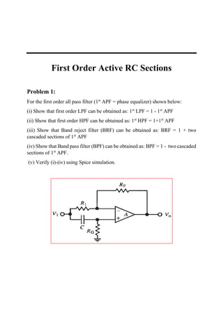
  • 1. First Order Active RC Sections Problem 1: For the first order all pass filter (1st APF = phase equalizer) shown below: (i) Show that first order LPF can be obtained as: 1st LPF = 1 - 1st APF (ii) Show that first order HPF can be obtained as: 1st HPF = 1+1st APF (iii) Show that Band reject filter (BRF) can be obtained as: BRF = 1 + two cascaded sections of 1st APF (iv) Show that Band pass filter (BPF) can be obtained as: BPF = 1 - two cascaded sections of 1st APF. (v) Verify (i)-(iv) using Spice simulation.
  • 2. First Order Active RC Sections Problem 1: For the first order all pass filter (1st APF) shown below: (i) Show that first order LPF can be obtained as: 1st LPF = 1 - 1st APF Solution: The transfer function of 1st APF is given by 𝑇(𝑆) = 𝑉𝑜𝑢𝑡 𝑉𝑖𝑛 = 𝑆𝐶 − 𝐺 𝐺 𝑆𝐶 + 𝐺 𝐺 = 𝑆 − 1 𝑅 𝐺 𝐶 𝑆 + 1 𝑅 𝐺 𝐶 = − 1 − 𝑆𝐶𝑅 𝐺 1 + 𝑆𝐶𝑅 𝐺 Using subtractor based on op-amp where two inputs of the subtractor circuit are the input voltage and the output of the 1st APF. The output of the subtractor is 𝑉𝑜1 𝑉𝑖𝑛 = 1 − (− 1 − 𝑆𝐶𝑅 𝐺 1 + 𝑆𝐶𝑅 𝐺 ) = ( 1 + 𝑆𝐶𝑅 𝐺 + 1 − 𝑆𝐶𝑅 𝐺 1 + 𝑆𝐶𝑅 𝐺 ) 𝑉𝑜1 𝑉𝑖𝑛 = ( 2 1 + 𝑆𝐶𝑅 𝐺 ) It is 1st order LPF. By using C = 0.1µF and RG = R = RF = 41.42kΩ: The Dc gain is Dc gain = 20 log(2) = 6dB the cut-off frequency is 𝜔 𝑜 = 1 𝐶𝑅 𝐺 = 241.42rad/ sec = 2𝜋 (38.4Hz)
  • 3. (ii) Show that first order LPF can be obtained as: 1st HPF = 1 +1st APF Solution: The transfer function of 1st APF is given by 𝑇(𝑆) = 𝑉𝑜𝑢𝑡 𝑉𝑖𝑛 = − 1 − 𝑆𝐶𝑅 𝐺 1 + 𝑆𝐶𝑅 𝐺 Using adder based on op-amp circuit where the two inputs of the adder circuit are the input voltage and the output of the 1st APF. The output of the adder is − 𝑉𝑜1 𝑉𝑖𝑛 = 1 + (− 1 − 𝑆𝐶𝑅 𝐺 1 + 𝑆𝐶𝑅 𝐺 ) = ( 1 + 𝑆𝐶𝑅 𝐺 − 1 + 𝑆𝐶𝑅 𝐺 1 + 𝑆𝐶𝑅 𝐺 ) − 𝑉𝑜1 𝑉𝑖𝑛 = ( 2𝑆𝐶𝑅 𝐺 1 + 𝑆𝐶𝑅 𝐺 ) It is 1st HPF. By using C = 0.1µF and RG = R = RF = 41.42kΩ: The Dc gain at 𝑇(𝑗𝜔 = ∞) is Dc gain = 20 log(2) = 6dB the cut-off frequency is 𝜔 𝑜 = 1 𝐶𝑅 𝐺 = 241.42rad/sec = 2π (38.4Hz)
  • 4. (iii) Show that Band reject filter (BRF) can be obtained as: BRF = 1 + two cascaded sections of 1st APF (BRF = 1 + 2nd APF) Solution: The transfer function of two cascaded section of 1st APF is given by 𝑇(𝑆) = (− 1 − 𝑆𝐶𝑅 𝐺 1 + 𝑆𝐶𝑅 𝐺 ) × (− 1 − 𝑆𝐶𝑅 𝐺 1 + 𝑆𝐶𝑅 𝐺 ) 𝑇(𝑆) = 1 − 2𝑆𝐶𝑅 𝐺 + (𝑆𝐶𝑅 𝐺)2 1 + 2𝑆𝐶𝑅 𝐺 + (𝑆𝐶𝑅 𝐺)2 It is a 2nd order APF. 𝜔𝑧 = 𝜔 𝑝 = 1 𝐶𝑅 𝐺 = 241.42 rad/sec = 2π (38.4Hz) Using adder based on op-amp circuit where the two inputs of the adder circuit are the input voltage and the output of the 2st order APF. The output of the adder is − 𝑉𝑜1 𝑉𝑖𝑛 = 1 + ( 1 − 2𝑆𝐶𝑅 𝐺 + (𝑆𝐶𝑅 𝐺)2 1 + 2𝑆𝐶𝑅 𝐺 + (𝑆𝐶𝑅 𝐺)2 ) − 𝑉𝑜1 𝑉𝑖𝑛 = 1 + 2𝑆𝐶𝑅 𝐺 + (𝑆𝐶𝑅 𝐺)2 + 1 − 2𝑆𝐶𝑅 𝐺 + (𝑆𝐶𝑅 𝐺)2 1 + 2𝑆𝐶𝑅 𝐺 + (𝑆𝐶𝑅 𝐺)2 − 𝑉𝑜1 𝑉𝑖𝑛 = 2 1 + (𝑆𝐶𝑅 𝐺)2 1 + 2𝑆𝐶𝑅 𝐺 + (𝑆𝐶𝑅 𝐺)2 It is 2nd order notch filter. By using C = 0.1µF and RG = R = RF = 41.42kΩ: In the two passbands ( ω → 0 and ω → ∞ ) the gain is Dc gain = 20 log(2) = 6dB while the notch frequency is 𝜔 𝑜 = 1 𝐶𝑅 𝐺 = 241.42rad/ sec = 2𝜋 (38.4Hz) The pole quality factor Q is obtained as 𝜔 𝑜 𝑄 = 2 𝐶𝑅 𝐺 𝑄 = 𝜔 𝑜 2/𝐶𝑅 𝐺 = 0.5
  • 5. 𝑄 = 𝜔 𝑜 𝐵𝑊 = 0.5 𝐵𝑊 = (𝜔2 − 𝜔1) = 𝜔 𝑜 𝑄 = 482.84 rad/ sec = 2𝜋 (76.89Hz) 𝐵𝑊 = (𝜔2 − 𝜔1) = 𝜔 𝑜 𝑄 = 482.84 rad/sec 𝜔 𝑜 = √ 𝜔1 𝜔2 = 241.42 rad/sec 𝜔2 = 𝜔1 + 𝐵𝑊 = 𝜔1 + 482.84 𝜔2 = 𝜔 𝑜 2 𝜔1 = (241.42)2 𝜔1 By substituting 𝜔2 𝜔1 + 482.84 = (241.42)2 𝜔1 𝜔1 2 + 482.84𝜔1 − (241.42)2 = 0 Either 𝜔1 = 100.123 rad/sec or 𝜔1 = −582.123 rad/sec (ignore) ∴ 𝜔1 = 100.123 rad/ sec = 2𝜋 (16Hz) → The lower cut-off frequency 𝜔2 = 𝜔1 + 𝐵𝑊 = 100.123 + 482.84 = 582.963 rad/ sec = 2𝜋 (93Hz) 𝜔2→ the higher cut-off frequency. The depth of the notch in dB can be found as |− 𝑉𝑜1 𝑉𝑖𝑛 | = |2| |1 + (𝑗𝜔𝐶𝑅 𝐺)2| |1 + 2𝑗𝜔𝐶𝑅 𝐺 + (𝑗𝜔𝐶𝑅 𝐺)2| |− 𝑉𝑜1 𝑉𝑖𝑛 | = |2| √(1 + −𝜔2 𝐶2 𝑅 𝐺 2 ) 2 √(1 − 𝜔2 𝐶2 𝑅 𝐺 2 ) 2 + (2𝜔𝐶𝑅 𝐺)2 At notch frequency 𝜔 = 𝜔 𝑜 = 1 𝐶𝑅 𝐺
  • 6. |− 𝑉𝑜1 𝑉𝑖𝑛 | = |2| √(1 + −𝜔2 𝐶2 𝑅 𝐺 2 ) 2 √(1 − 𝜔 𝑜 2 𝐶2 𝑅 𝐺 2 ) 2 + (2𝜔 𝑜 𝐶𝑅 𝐺)2 = 0 But practically we need to assume that there exists mismatch between simulated cut-off frequency ωo,sim and calculated one 1/CRG due to their tolerances (inaccurate component values) and may include PVT mismatches (the assumed error value between calculated ωo and simulated ωo is about 1.1%): 𝑒𝑟𝑟𝑜𝑟 = (𝜔 𝑜,𝑐𝑎𝑙 − 𝜔 𝑜,𝑠𝑖𝑚) 𝜔 𝑜,𝑐𝑎𝑙 × 100% 1.1% = (241.42 − 𝜔 𝑜,𝑠𝑖𝑚) 241.42 × 100% 𝜔 𝑜,𝑠𝑖𝑚 = 238.75rad/sec Now, the depth of the notch is |− 𝑉𝑜1 𝑉𝑖𝑛 | = 2 √(1 − (238.75 × 0.004142)2)2 √(1 − (238.75 × 0.004142)2)2 + (2 × 238.75 × 0.004142)2 |− 𝑉𝑜1 𝑉𝑖𝑛 | = 2 0.02207 √(0.02207)2 + (1.9778)2 |− 𝑉𝑜1 𝑉𝑖𝑛 | = 2 0.02207 1.9779 = 0.02232 The notch depth in dB is 20log |− Vo1 Vin | = 20 log(0.02232) = −33dB The notch rejection (the notch attenuation) is around 33dB. If we use ω = ωo = 241.42rad/sec (approximated calculated value), then |− 𝑉𝑜1 𝑉𝑖𝑛 | = 2 √(1 − (241.42 × 0.004142)2)2 √(1 − (241.42 × 0.004142)2)2 + (2 × 241.42 × 0.004142)2 |− 𝑉𝑜1 𝑉𝑖𝑛 | = 2 0.000076719 √(1 − 0.9999)2 + (1.9999)2 = 7.6719 × 10⁻⁵ The notch depth in dB is
  • 7. 20log |− Vo1 Vin | = 20 log(7.6719 × 10⁻⁵) = −82dB The gain at the lower cut-off frequency ω1 is |− 𝑉𝑜1 𝑉𝑖𝑛 | = 2 √(1 − (100.123 × 0.004142)2)2 √(1 − (100.123 × 0.004142)2)2 + (2 × 100.123 × 0.004142)2 |− 𝑉𝑜1 𝑉𝑖𝑛 | = 2 0.8280 √(0.8280)2 + (0.8294)2 = 1.413 𝑉/𝑉 The gain at the higher cut-off frequency ω2 is |− 𝑉𝑜1 𝑉𝑖𝑛 | = 2 √(1 − (583.123 × 0.004142)2)2 √(1 − (583.123 × 0.004142)2)2 + (2 × 583.123 × 0.004142)2 |− 𝑉𝑜1 𝑉𝑖𝑛 | = 2 4.834 √(4.834)2 + (4.831)2 = 1.415 𝑉/𝑉 The gain in dB at both frequency is 3dB.
  • 8. (iv) Show that Band pass filter (BPF) can be obtained as: BPF = 1 - two cascaded sections of 1st APF (BBF = 1 - 2nd APF) Solution: The transfer function of two cascaded section of 1st APF is given by 𝑇(𝑆) = 1 − 2𝑆𝐶𝑅 𝐺 + (𝑆𝐶𝑅 𝐺)2 1 + 2𝑆𝐶𝑅 𝐺 + (𝑆𝐶𝑅 𝐺)2 It is a 2nd order APF. 𝜔𝑧 = 𝜔 𝑝 = 1 𝐶𝑅 𝐺 = 241.42 rad/sec = 2π (38.4Hz) Using subtractor based on op-amp circuit where the two inputs of the subtractor circuit are the input voltage and the output of the 2st order APF. The output of the subtractor is 𝑉𝑜1 𝑉𝑖𝑛 = 1 − ( 1 − 2𝑆𝐶𝑅 𝐺 + (𝑆𝐶𝑅 𝐺)2 1 + 2𝑆𝐶𝑅 𝐺 + (𝑆𝐶𝑅 𝐺)2 ) 𝑉𝑜1 𝑉𝑖𝑛 = 1 + 2𝑆𝐶𝑅 𝐺 + (𝑆𝐶𝑅 𝐺)2 − 1 + 2𝑆𝐶𝑅 𝐺 − (𝑆𝐶𝑅 𝐺)2 1 + 2𝑆𝐶𝑅 𝐺 + (𝑆𝐶𝑅 𝐺)2 𝑉𝑜1 𝑉𝑖𝑛 = 4𝑆𝐶𝑅 𝐺 1 + 2𝑆𝐶𝑅 𝐺 + (𝑆𝐶𝑅 𝐺)2 It is 2nd order BPF. By using C = 0.1µF and RG = R = RF = 41.42kΩ: In the two passbands ( ω → 0 and ω → ∞) the gain is 0dB, while the center frequency is 𝜔 𝑜 = 1 𝐶𝑅 𝐺 = 241.42 rad/sec = 2π (38.4Hz) The pole quality factor Q is obtained as 𝜔 𝑜 𝑄 = 2 𝐶𝑅 𝐺 𝑄 = 𝜔 𝑜 2/𝐶𝑅 𝐺 = 0.5 𝑄 = 𝜔 𝑜 𝐵𝑊 = 0.5 𝐵𝑊 = (𝜔2 − 𝜔1) = 𝜔 𝑜 𝑄 = 482.84 rad/ sec = 2𝜋 (76.89Hz)
  • 9. 𝐵𝑊 = (𝜔2 − 𝜔1) = 𝜔 𝑜 𝑄 = 482.84 rad/sec 𝜔 𝑜 = √ 𝜔1 𝜔2 = 241.42 rad/sec 𝜔2 = 𝜔1 + 𝐵𝑊 = 𝜔1 + 482.84 𝜔2 = 𝜔 𝑜 2 𝜔1 = (241.42)2 𝜔1 By substituting 𝜔2 𝜔1 + 482.84 = (241.42)2 𝜔1 𝜔1 2 + 482.84𝜔1 − (241.42)2 = 0 Either 𝜔1 = 100.123 rad/sec or 𝜔1 = −582.123 rad/sec (ignore) ∴ 𝜔1 = 100.123 rad/ sec = 2𝜋 (16Hz) → The lower cut-off frequency 𝜔2 = 𝜔1 + 𝐵𝑊 = 100.123 + 482.84 = 582.963 rad/ sec = 2𝜋 (93Hz) 𝜔2→ the upper cut-off frequency. The gain at the center frequency 𝜔 𝑜 = 1 𝐶𝑅 𝐺 can be found as |− 𝑉𝑜1 𝑉𝑖𝑛 | = 4 |𝑗𝜔𝐶𝑅 𝐺| |1 + 2𝑗𝜔𝐶𝑅 𝐺 + (𝑗𝜔𝐶𝑅 𝐺)2| |− 𝑉𝑜1 𝑉𝑖𝑛 | = 4 √(𝜔𝐶𝑅 𝐺)2 √(1 − 𝜔2 𝐶2 𝑅 𝐺 2 ) 2 + (2𝜔𝐶𝑅 𝐺)2 |− 𝑉𝑜1 𝑉𝑖𝑛 | = 4 √(1)2 √(0)2 + (2)2 |− 𝑉𝑜1 𝑉𝑖𝑛 | = 4 1 2 = 2 𝑉/𝑉 The gain in dB is 20log |− Vo1 Vin | = 20 log(2) = 6dB
  • 10. (v) Verify (i)-(iv) using Spice simulation. LTspice simulation for (i) 1st LPF:
  • 11. LTspice simulation for (ii) 1st HPF:
  • 12. LTspice simulation for (iii) 2st BRF:
  • 13.
  • 14. LTspice simulation for (iv) 2st BPF: