SlideShare ist ein Scribd-Unternehmen logo
1 von 5
Downloaden Sie, um offline zu lesen
DSD and HDL Simulation, Assignment Questions
Problem Implement following functions using Xilinx XC 3000. How many CLBs and LUTs are
required?
𝒀 = 𝒙̅ + 𝒚 ; 𝒀 = 𝒙 𝒚̅̅̅ + 𝒙̅ 𝒚̅̅̅ ; 𝒛 = 𝒙 . 𝒚
where 𝒀 , 𝒀 are the next state variables and 𝒚 , 𝒚 are the present state variables. Here, x
and z are input and output respectively.
Solution: The sequential circuit has 3 input variables.
Note that FG mode can implement two functions of four variables each. Hence, using FG mode of
operation, 2 CLBs and 3 LUTs are required.
The simplified internal circuit diagram of XC 3000 CLB in FG mode is shown below:
The LUT contents are shown below:
For = ̅ +
Address Memory content
(F of CLB1)
x 𝒚 𝒀
0 0 1
0 1 1
1 0 0
1 1 1
For = ̅̅̅ + ̅ ̅̅̅
Address Memory content
(G of CLB1)
x 𝒚 𝒚 𝒀
0 0 0 1
0 0 1 1
0 1 0 0
0 1 1 0
1 0 0 1
1 0 1 0
1 1 0 1
1 1 1 0
DR
CLB
OUTPUTs
G
FG1 F
Qy
CLK
GFG2
Q2
D1
F
D2
G
Q1
Qx
F
For 𝑧 = .
Address Memory content
(F of CLB2)
x 𝒚 𝒀
0 0 0
0 1 0
1 0 0
1 1 1
Circuit implementation using two XC3000 CLBs is shown below:
-----------------------------------------------------------------------------------------------------------------------------------------
Problem Consider a 2 bit magnitude comparator to compare 𝐴 𝐴 and 𝐵 𝐵 to define three
outputs A>B, A<B, A=B and map it using Xilinx XC 3000 FPGA. How many CLBs and LUTs are
required? Show the contents of sRAM cell
Solution:
Consider the truth table for output A=B
Y1
Q1
D2
Q1
Q2
Q2
DR
G
y1
CLK
G
G
F
Y2
G
z
FG2
FG1
CLB 2
x
Qx
y1
Qy
DR
x
y1
CLB 1
y2
D2
FG1 F
x
F
FG2
CLK
Qy
D1
D1
F
Qx
𝐴 𝐴 𝐵 𝐵 EQ
0 0 0 0 1
0 1 0 1 1
1 0 1 0 1
1 1 1 1 1
Design equation for EQ is
𝐸𝑄 = 𝐴̅̅̅ 𝐴̅̅̅ 𝐵̅̅̅ 𝐵̅̅̅ + 𝐴̅̅̅ 𝐴 𝐵̅̅̅ 𝐵 + 𝐴 𝐴̅̅̅ 𝐵 𝐵̅̅̅ + 𝐴 𝐴 𝐵 𝐵
Consider the truth table for output A>B
𝐴 𝐴 𝐵 𝐵 A>B
1 X 0 X 1
0 1 0 0 1
1 1 1 0 1
The corresponding implicant table is
𝐴 𝐴 𝐵 𝐵 A>B
1 X 0 X 1
X 1 0 0 1
1 1 X 0 1
Design equation for A>B is
𝐴 > 𝐵 = 𝐴 𝐵̅̅̅ + 𝐴 𝐵̅̅̅ 𝐵̅̅̅ + 𝐴 𝐴 𝐵̅̅̅
Consider the truth table for output A<B
𝐴 𝐴 𝐵 𝐵 A<B
0 X 1 X 1
0 0 0 1 1
1 0 1 1 1
The corresponding implicant table is
𝐴 𝐴 𝐵 𝐵 A<B
0 X 1 X 1
0 0 X 1 1
X 0 1 1 1
Design equation for A<B is
𝐴 < 𝐵 = 𝐴̅̅̅ 𝐵 + 𝐴̅̅̅. 𝐴̅̅̅̅. 𝐵 + 𝐴̅̅̅̅ 𝐵 𝐵
2 bit magnitude comparator has 4 input variables and 3 outputs. The circuit implementation
using XC 3000 in FG mode requires 2 CLBs and 3 LUTs.
Circuit implementation using two XC3000 CLBs is shown below:
The LUT (LUT1 and LUT2 of two CLBs) contents are given below:
G
A0
B1
LUT1
FG mode
B0
F
F
A0
Qy
Qy
B1
CLK
CLK
G
A>B
G
A1
A=B
B1
Q2
Q2
A<B
B0
D1
D1
A1
D2
D2
A0
Q1
Q1
B0
Qx
Qx
LUT2
F
F
FG mode
DR
CLB 1
LUT1
CLB 2
DR
A1
LUT2 G
Address Memory
content
(F of CLB1)
Memory
content
(G of CLB1)
Memory
content
(F of CLB2)
> = <
0 0 0 0 0 1 0
0 0 0 1 0 0 1
0 0 1 0 0 0 1
0 0 1 1 0 0 1
0 1 0 0 1 0 0
0 1 0 1 0 1 0
0 1 1 0 0 0 0
0 1 1 1 0 0 0
1 0 0 0 1 0 0
1 0 0 1 1 0 0
1 0 1 0 0 1 0
1 0 1 1 0 0 1
1 1 0 0 0 0 0
1 1 0 1 0 0 0
1 1 1 0 1 0 0
1 1 1 1 0 1 0
------------------------------------------------------------------------------------------------------------------------------
Problem Implement following function using Xilinx XC 3000. How many CLBs and LUTs are
required? F(a, b, c, d, e) = a. b. c + a. b̅. c + e̅ + d. e
Solution: The output function has 5 input variables. The circuit implementation using XC 3000 in F
mode (Note that F mode can generate one function of five variables) requires 1 CLB and 1 LUT.
Problem Implement 2421 to 8421 code converter using Xilinx XC 3000. How many CLBs and
LUTs are required? Show the contents of the sRAM cell.
Dr. D. V. Kamath
Professor, Dept. of E&C Engg., MIT
LUT
F
F
G
b
e
Q2
DR CLB 1
Qy
CLK
D1
F
F
Qx
Q1
G
a
D2
c
d
F mode

Weitere ähnliche Inhalte

Was ist angesagt?

Fpga(field programmable gate array)
Fpga(field programmable gate array) Fpga(field programmable gate array)
Fpga(field programmable gate array)
Iffat Anjum
 
Xilinx lca and altera flex
Xilinx lca and altera flexXilinx lca and altera flex
Xilinx lca and altera flex
anishgoel
 

Was ist angesagt? (20)

Fpga(field programmable gate array)
Fpga(field programmable gate array) Fpga(field programmable gate array)
Fpga(field programmable gate array)
 
Programmable logic array
Programmable logic arrayProgrammable logic array
Programmable logic array
 
Unit VI CPLD-FPGA Architecture
Unit VI CPLD-FPGA ArchitectureUnit VI CPLD-FPGA Architecture
Unit VI CPLD-FPGA Architecture
 
VLSI Design Sequential circuit design
VLSI Design Sequential circuit designVLSI Design Sequential circuit design
VLSI Design Sequential circuit design
 
Logic Synthesis
Logic SynthesisLogic Synthesis
Logic Synthesis
 
FPGA
FPGAFPGA
FPGA
 
Fundamentals of FPGA
Fundamentals of FPGAFundamentals of FPGA
Fundamentals of FPGA
 
Seminar on field programmable gate array
Seminar on field programmable gate arraySeminar on field programmable gate array
Seminar on field programmable gate array
 
Smart traffic light controller using verilog
Smart traffic light controller using verilogSmart traffic light controller using verilog
Smart traffic light controller using verilog
 
VHDL-PRESENTATION.ppt
VHDL-PRESENTATION.pptVHDL-PRESENTATION.ppt
VHDL-PRESENTATION.ppt
 
DSP_2018_FOEHU - Lec 04 - The z-Transform
DSP_2018_FOEHU - Lec 04 - The z-TransformDSP_2018_FOEHU - Lec 04 - The z-Transform
DSP_2018_FOEHU - Lec 04 - The z-Transform
 
Design options for digital systems
Design options for digital systemsDesign options for digital systems
Design options for digital systems
 
Introduction to FPGAs
Introduction to FPGAsIntroduction to FPGAs
Introduction to FPGAs
 
Xilinx lca and altera flex
Xilinx lca and altera flexXilinx lca and altera flex
Xilinx lca and altera flex
 
PLDs
PLDsPLDs
PLDs
 
Simulation power analysis low power vlsi
Simulation power analysis   low power vlsiSimulation power analysis   low power vlsi
Simulation power analysis low power vlsi
 
Pipeline processing and space time diagram
Pipeline processing and space time diagramPipeline processing and space time diagram
Pipeline processing and space time diagram
 
Fpga Knowledge
Fpga KnowledgeFpga Knowledge
Fpga Knowledge
 
Verilog tutorial
Verilog tutorialVerilog tutorial
Verilog tutorial
 
Kernighan lin
Kernighan linKernighan lin
Kernighan lin
 

Andere mochten auch

vlsi design flow
vlsi design flowvlsi design flow
vlsi design flow
Anish Gupta
 
prom,pld problems
prom,pld problemsprom,pld problems
prom,pld problems
Anish Gupta
 
Testing boolean difference
Testing boolean differenceTesting boolean difference
Testing boolean difference
Anish Gupta
 
Booth multiplication
Booth multiplicationBooth multiplication
Booth multiplication
M Madan Gopal
 

Andere mochten auch (20)

DSD
DSDDSD
DSD
 
vlsi design flow
vlsi design flowvlsi design flow
vlsi design flow
 
cplds
cpldscplds
cplds
 
prom,pld problems
prom,pld problemsprom,pld problems
prom,pld problems
 
Testing boolean difference
Testing boolean differenceTesting boolean difference
Testing boolean difference
 
Spartan-II FPGA (xc2s30)
Spartan-II FPGA (xc2s30)Spartan-II FPGA (xc2s30)
Spartan-II FPGA (xc2s30)
 
UNIT-III-DIGITAL SYSTEM DESIGN
UNIT-III-DIGITAL SYSTEM DESIGNUNIT-III-DIGITAL SYSTEM DESIGN
UNIT-III-DIGITAL SYSTEM DESIGN
 
Dsd previous year university questions
Dsd previous year university questionsDsd previous year university questions
Dsd previous year university questions
 
Esc At Actel So C Ver3
Esc At Actel So C  Ver3Esc At Actel So C  Ver3
Esc At Actel So C Ver3
 
Fpga 03-cpld-and-fpga
Fpga 03-cpld-and-fpgaFpga 03-cpld-and-fpga
Fpga 03-cpld-and-fpga
 
Booth multiplication
Booth multiplicationBooth multiplication
Booth multiplication
 
Semiconductor Hubs for Research & Innovation
Semiconductor Hubs for Research & InnovationSemiconductor Hubs for Research & Innovation
Semiconductor Hubs for Research & Innovation
 
Power
PowerPower
Power
 
System on chip architectures
System on chip architecturesSystem on chip architectures
System on chip architectures
 
Soc architecture and design
Soc architecture and designSoc architecture and design
Soc architecture and design
 
Processors used in System on chip
Processors used in System on chip Processors used in System on chip
Processors used in System on chip
 
How to Make Effective Presentation
How to Make Effective PresentationHow to Make Effective Presentation
How to Make Effective Presentation
 
System on chip buses
System on chip busesSystem on chip buses
System on chip buses
 
SOC Peripheral Components & SOC Tools
SOC Peripheral Components & SOC ToolsSOC Peripheral Components & SOC Tools
SOC Peripheral Components & SOC Tools
 
Processors selection
Processors selectionProcessors selection
Processors selection
 

Ähnlich wie xilinx fpga problems

Sequential Circuitsdddddddddddddddddsssssssssss-ppt.pptx
Sequential Circuitsdddddddddddddddddsssssssssss-ppt.pptxSequential Circuitsdddddddddddddddddsssssssssss-ppt.pptx
Sequential Circuitsdddddddddddddddddsssssssssss-ppt.pptx
AhmedAlAfandi5
 
Binary Adder Design(COA).ppt
Binary Adder Design(COA).pptBinary Adder Design(COA).ppt
Binary Adder Design(COA).ppt
RohitPaul71
 
Electrónica digital: Diseño de contador con flip-flop tipo JK y D haciendo de...
Electrónica digital: Diseño de contador con flip-flop tipo JK y D haciendo de...Electrónica digital: Diseño de contador con flip-flop tipo JK y D haciendo de...
Electrónica digital: Diseño de contador con flip-flop tipo JK y D haciendo de...
SANTIAGO PABLO ALBERTO
 
SEQUENTIAL CIRCUITS -Module 5 (1).pptx
SEQUENTIAL CIRCUITS -Module 5 (1).pptxSEQUENTIAL CIRCUITS -Module 5 (1).pptx
SEQUENTIAL CIRCUITS -Module 5 (1).pptx
ThanmayiKumar
 
CSCMPE 3430, sp16 – Assignment 5 (30 points total) Due S.docx
CSCMPE 3430, sp16 – Assignment 5 (30 points total) Due S.docxCSCMPE 3430, sp16 – Assignment 5 (30 points total) Due S.docx
CSCMPE 3430, sp16 – Assignment 5 (30 points total) Due S.docx
annettsparrow
 

Ähnlich wie xilinx fpga problems (20)

Sequential Circuitsdddddddddddddddddsssssssssss-ppt.pptx
Sequential Circuitsdddddddddddddddddsssssssssss-ppt.pptxSequential Circuitsdddddddddddddddddsssssssssss-ppt.pptx
Sequential Circuitsdddddddddddddddddsssssssssss-ppt.pptx
 
Sequential Circuits-ppt_2.pdf
Sequential Circuits-ppt_2.pdfSequential Circuits-ppt_2.pdf
Sequential Circuits-ppt_2.pdf
 
elec2200-6.pdf
elec2200-6.pdfelec2200-6.pdf
elec2200-6.pdf
 
End sem solution
End sem solutionEnd sem solution
End sem solution
 
Sequential logic circuit
Sequential logic circuitSequential logic circuit
Sequential logic circuit
 
F010113644
F010113644F010113644
F010113644
 
Multiplier and Accumulator Using Csla
Multiplier and Accumulator Using CslaMultiplier and Accumulator Using Csla
Multiplier and Accumulator Using Csla
 
Lec9
Lec9Lec9
Lec9
 
1سلمي 2
1سلمي 21سلمي 2
1سلمي 2
 
Binary Adder Design(COA).ppt
Binary Adder Design(COA).pptBinary Adder Design(COA).ppt
Binary Adder Design(COA).ppt
 
Conversion of flip flop
Conversion of flip flopConversion of flip flop
Conversion of flip flop
 
Electrónica digital: Diseño de contador con flip-flop tipo JK y D haciendo de...
Electrónica digital: Diseño de contador con flip-flop tipo JK y D haciendo de...Electrónica digital: Diseño de contador con flip-flop tipo JK y D haciendo de...
Electrónica digital: Diseño de contador con flip-flop tipo JK y D haciendo de...
 
Lec16 Intro to Computer Engineering by Hsien-Hsin Sean Lee Georgia Tech -- Fi...
Lec16 Intro to Computer Engineering by Hsien-Hsin Sean Lee Georgia Tech -- Fi...Lec16 Intro to Computer Engineering by Hsien-Hsin Sean Lee Georgia Tech -- Fi...
Lec16 Intro to Computer Engineering by Hsien-Hsin Sean Lee Georgia Tech -- Fi...
 
jana2012.pdf
jana2012.pdfjana2012.pdf
jana2012.pdf
 
UNIT - II.pptx
UNIT - II.pptxUNIT - II.pptx
UNIT - II.pptx
 
SEQUENTIAL CIRCUITS -Module 5 (1).pptx
SEQUENTIAL CIRCUITS -Module 5 (1).pptxSEQUENTIAL CIRCUITS -Module 5 (1).pptx
SEQUENTIAL CIRCUITS -Module 5 (1).pptx
 
Digital Logic circuit
Digital Logic circuitDigital Logic circuit
Digital Logic circuit
 
CSLA and WTM using GDI Technique
CSLA and WTM using GDI TechniqueCSLA and WTM using GDI Technique
CSLA and WTM using GDI Technique
 
Analysis sequential circuits
Analysis sequential circuitsAnalysis sequential circuits
Analysis sequential circuits
 
CSCMPE 3430, sp16 – Assignment 5 (30 points total) Due S.docx
CSCMPE 3430, sp16 – Assignment 5 (30 points total) Due S.docxCSCMPE 3430, sp16 – Assignment 5 (30 points total) Due S.docx
CSCMPE 3430, sp16 – Assignment 5 (30 points total) Due S.docx
 

Kürzlich hochgeladen

Call for Papers - Educational Administration: Theory and Practice, E-ISSN: 21...
Call for Papers - Educational Administration: Theory and Practice, E-ISSN: 21...Call for Papers - Educational Administration: Theory and Practice, E-ISSN: 21...
Call for Papers - Educational Administration: Theory and Practice, E-ISSN: 21...
Christo Ananth
 
Call Girls In Bangalore ☎ 7737669865 🥵 Book Your One night Stand
Call Girls In Bangalore ☎ 7737669865 🥵 Book Your One night StandCall Girls In Bangalore ☎ 7737669865 🥵 Book Your One night Stand
Call Girls In Bangalore ☎ 7737669865 🥵 Book Your One night Stand
amitlee9823
 
notes on Evolution Of Analytic Scalability.ppt
notes on Evolution Of Analytic Scalability.pptnotes on Evolution Of Analytic Scalability.ppt
notes on Evolution Of Analytic Scalability.ppt
MsecMca
 
Call Now ≽ 9953056974 ≼🔝 Call Girls In New Ashok Nagar ≼🔝 Delhi door step de...
Call Now ≽ 9953056974 ≼🔝 Call Girls In New Ashok Nagar  ≼🔝 Delhi door step de...Call Now ≽ 9953056974 ≼🔝 Call Girls In New Ashok Nagar  ≼🔝 Delhi door step de...
Call Now ≽ 9953056974 ≼🔝 Call Girls In New Ashok Nagar ≼🔝 Delhi door step de...
9953056974 Low Rate Call Girls In Saket, Delhi NCR
 

Kürzlich hochgeladen (20)

Call Girls Walvekar Nagar Call Me 7737669865 Budget Friendly No Advance Booking
Call Girls Walvekar Nagar Call Me 7737669865 Budget Friendly No Advance BookingCall Girls Walvekar Nagar Call Me 7737669865 Budget Friendly No Advance Booking
Call Girls Walvekar Nagar Call Me 7737669865 Budget Friendly No Advance Booking
 
Call Girls Pimpri Chinchwad Call Me 7737669865 Budget Friendly No Advance Boo...
Call Girls Pimpri Chinchwad Call Me 7737669865 Budget Friendly No Advance Boo...Call Girls Pimpri Chinchwad Call Me 7737669865 Budget Friendly No Advance Boo...
Call Girls Pimpri Chinchwad Call Me 7737669865 Budget Friendly No Advance Boo...
 
PVC VS. FIBERGLASS (FRP) GRAVITY SEWER - UNI BELL
PVC VS. FIBERGLASS (FRP) GRAVITY SEWER - UNI BELLPVC VS. FIBERGLASS (FRP) GRAVITY SEWER - UNI BELL
PVC VS. FIBERGLASS (FRP) GRAVITY SEWER - UNI BELL
 
data_management_and _data_science_cheat_sheet.pdf
data_management_and _data_science_cheat_sheet.pdfdata_management_and _data_science_cheat_sheet.pdf
data_management_and _data_science_cheat_sheet.pdf
 
Call for Papers - Educational Administration: Theory and Practice, E-ISSN: 21...
Call for Papers - Educational Administration: Theory and Practice, E-ISSN: 21...Call for Papers - Educational Administration: Theory and Practice, E-ISSN: 21...
Call for Papers - Educational Administration: Theory and Practice, E-ISSN: 21...
 
CCS335 _ Neural Networks and Deep Learning Laboratory_Lab Complete Record
CCS335 _ Neural Networks and Deep Learning Laboratory_Lab Complete RecordCCS335 _ Neural Networks and Deep Learning Laboratory_Lab Complete Record
CCS335 _ Neural Networks and Deep Learning Laboratory_Lab Complete Record
 
Call Girls In Bangalore ☎ 7737669865 🥵 Book Your One night Stand
Call Girls In Bangalore ☎ 7737669865 🥵 Book Your One night StandCall Girls In Bangalore ☎ 7737669865 🥵 Book Your One night Stand
Call Girls In Bangalore ☎ 7737669865 🥵 Book Your One night Stand
 
notes on Evolution Of Analytic Scalability.ppt
notes on Evolution Of Analytic Scalability.pptnotes on Evolution Of Analytic Scalability.ppt
notes on Evolution Of Analytic Scalability.ppt
 
Unit 1 - Soil Classification and Compaction.pdf
Unit 1 - Soil Classification and Compaction.pdfUnit 1 - Soil Classification and Compaction.pdf
Unit 1 - Soil Classification and Compaction.pdf
 
(INDIRA) Call Girl Aurangabad Call Now 8617697112 Aurangabad Escorts 24x7
(INDIRA) Call Girl Aurangabad Call Now 8617697112 Aurangabad Escorts 24x7(INDIRA) Call Girl Aurangabad Call Now 8617697112 Aurangabad Escorts 24x7
(INDIRA) Call Girl Aurangabad Call Now 8617697112 Aurangabad Escorts 24x7
 
The Most Attractive Pune Call Girls Budhwar Peth 8250192130 Will You Miss Thi...
The Most Attractive Pune Call Girls Budhwar Peth 8250192130 Will You Miss Thi...The Most Attractive Pune Call Girls Budhwar Peth 8250192130 Will You Miss Thi...
The Most Attractive Pune Call Girls Budhwar Peth 8250192130 Will You Miss Thi...
 
Thermal Engineering-R & A / C - unit - V
Thermal Engineering-R & A / C - unit - VThermal Engineering-R & A / C - unit - V
Thermal Engineering-R & A / C - unit - V
 
Booking open Available Pune Call Girls Pargaon 6297143586 Call Hot Indian Gi...
Booking open Available Pune Call Girls Pargaon  6297143586 Call Hot Indian Gi...Booking open Available Pune Call Girls Pargaon  6297143586 Call Hot Indian Gi...
Booking open Available Pune Call Girls Pargaon 6297143586 Call Hot Indian Gi...
 
Call Now ≽ 9953056974 ≼🔝 Call Girls In New Ashok Nagar ≼🔝 Delhi door step de...
Call Now ≽ 9953056974 ≼🔝 Call Girls In New Ashok Nagar  ≼🔝 Delhi door step de...Call Now ≽ 9953056974 ≼🔝 Call Girls In New Ashok Nagar  ≼🔝 Delhi door step de...
Call Now ≽ 9953056974 ≼🔝 Call Girls In New Ashok Nagar ≼🔝 Delhi door step de...
 
Booking open Available Pune Call Girls Koregaon Park 6297143586 Call Hot Ind...
Booking open Available Pune Call Girls Koregaon Park  6297143586 Call Hot Ind...Booking open Available Pune Call Girls Koregaon Park  6297143586 Call Hot Ind...
Booking open Available Pune Call Girls Koregaon Park 6297143586 Call Hot Ind...
 
Water Industry Process Automation & Control Monthly - April 2024
Water Industry Process Automation & Control Monthly - April 2024Water Industry Process Automation & Control Monthly - April 2024
Water Industry Process Automation & Control Monthly - April 2024
 
Roadmap to Membership of RICS - Pathways and Routes
Roadmap to Membership of RICS - Pathways and RoutesRoadmap to Membership of RICS - Pathways and Routes
Roadmap to Membership of RICS - Pathways and Routes
 
Call for Papers - International Journal of Intelligent Systems and Applicatio...
Call for Papers - International Journal of Intelligent Systems and Applicatio...Call for Papers - International Journal of Intelligent Systems and Applicatio...
Call for Papers - International Journal of Intelligent Systems and Applicatio...
 
Double rodded leveling 1 pdf activity 01
Double rodded leveling 1 pdf activity 01Double rodded leveling 1 pdf activity 01
Double rodded leveling 1 pdf activity 01
 
Call Girls Wakad Call Me 7737669865 Budget Friendly No Advance Booking
Call Girls Wakad Call Me 7737669865 Budget Friendly No Advance BookingCall Girls Wakad Call Me 7737669865 Budget Friendly No Advance Booking
Call Girls Wakad Call Me 7737669865 Budget Friendly No Advance Booking
 

xilinx fpga problems

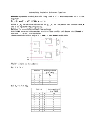
  • 1. DSD and HDL Simulation, Assignment Questions Problem Implement following functions using Xilinx XC 3000. How many CLBs and LUTs are required? 𝒀 = 𝒙̅ + 𝒚 ; 𝒀 = 𝒙 𝒚̅̅̅ + 𝒙̅ 𝒚̅̅̅ ; 𝒛 = 𝒙 . 𝒚 where 𝒀 , 𝒀 are the next state variables and 𝒚 , 𝒚 are the present state variables. Here, x and z are input and output respectively. Solution: The sequential circuit has 3 input variables. Note that FG mode can implement two functions of four variables each. Hence, using FG mode of operation, 2 CLBs and 3 LUTs are required. The simplified internal circuit diagram of XC 3000 CLB in FG mode is shown below: The LUT contents are shown below: For = ̅ + Address Memory content (F of CLB1) x 𝒚 𝒀 0 0 1 0 1 1 1 0 0 1 1 1 For = ̅̅̅ + ̅ ̅̅̅ Address Memory content (G of CLB1) x 𝒚 𝒚 𝒀 0 0 0 1 0 0 1 1 0 1 0 0 0 1 1 0 1 0 0 1 1 0 1 0 1 1 0 1 1 1 1 0 DR CLB OUTPUTs G FG1 F Qy CLK GFG2 Q2 D1 F D2 G Q1 Qx F
  • 2. For 𝑧 = . Address Memory content (F of CLB2) x 𝒚 𝒀 0 0 0 0 1 0 1 0 0 1 1 1 Circuit implementation using two XC3000 CLBs is shown below: ----------------------------------------------------------------------------------------------------------------------------------------- Problem Consider a 2 bit magnitude comparator to compare 𝐴 𝐴 and 𝐵 𝐵 to define three outputs A>B, A<B, A=B and map it using Xilinx XC 3000 FPGA. How many CLBs and LUTs are required? Show the contents of sRAM cell Solution: Consider the truth table for output A=B Y1 Q1 D2 Q1 Q2 Q2 DR G y1 CLK G G F Y2 G z FG2 FG1 CLB 2 x Qx y1 Qy DR x y1 CLB 1 y2 D2 FG1 F x F FG2 CLK Qy D1 D1 F Qx
  • 3. 𝐴 𝐴 𝐵 𝐵 EQ 0 0 0 0 1 0 1 0 1 1 1 0 1 0 1 1 1 1 1 1 Design equation for EQ is 𝐸𝑄 = 𝐴̅̅̅ 𝐴̅̅̅ 𝐵̅̅̅ 𝐵̅̅̅ + 𝐴̅̅̅ 𝐴 𝐵̅̅̅ 𝐵 + 𝐴 𝐴̅̅̅ 𝐵 𝐵̅̅̅ + 𝐴 𝐴 𝐵 𝐵 Consider the truth table for output A>B 𝐴 𝐴 𝐵 𝐵 A>B 1 X 0 X 1 0 1 0 0 1 1 1 1 0 1 The corresponding implicant table is 𝐴 𝐴 𝐵 𝐵 A>B 1 X 0 X 1 X 1 0 0 1 1 1 X 0 1 Design equation for A>B is 𝐴 > 𝐵 = 𝐴 𝐵̅̅̅ + 𝐴 𝐵̅̅̅ 𝐵̅̅̅ + 𝐴 𝐴 𝐵̅̅̅ Consider the truth table for output A<B 𝐴 𝐴 𝐵 𝐵 A<B 0 X 1 X 1 0 0 0 1 1 1 0 1 1 1 The corresponding implicant table is 𝐴 𝐴 𝐵 𝐵 A<B 0 X 1 X 1 0 0 X 1 1 X 0 1 1 1 Design equation for A<B is 𝐴 < 𝐵 = 𝐴̅̅̅ 𝐵 + 𝐴̅̅̅. 𝐴̅̅̅̅. 𝐵 + 𝐴̅̅̅̅ 𝐵 𝐵
  • 4. 2 bit magnitude comparator has 4 input variables and 3 outputs. The circuit implementation using XC 3000 in FG mode requires 2 CLBs and 3 LUTs. Circuit implementation using two XC3000 CLBs is shown below: The LUT (LUT1 and LUT2 of two CLBs) contents are given below: G A0 B1 LUT1 FG mode B0 F F A0 Qy Qy B1 CLK CLK G A>B G A1 A=B B1 Q2 Q2 A<B B0 D1 D1 A1 D2 D2 A0 Q1 Q1 B0 Qx Qx LUT2 F F FG mode DR CLB 1 LUT1 CLB 2 DR A1 LUT2 G
  • 5. Address Memory content (F of CLB1) Memory content (G of CLB1) Memory content (F of CLB2) > = < 0 0 0 0 0 1 0 0 0 0 1 0 0 1 0 0 1 0 0 0 1 0 0 1 1 0 0 1 0 1 0 0 1 0 0 0 1 0 1 0 1 0 0 1 1 0 0 0 0 0 1 1 1 0 0 0 1 0 0 0 1 0 0 1 0 0 1 1 0 0 1 0 1 0 0 1 0 1 0 1 1 0 0 1 1 1 0 0 0 0 0 1 1 0 1 0 0 0 1 1 1 0 1 0 0 1 1 1 1 0 1 0 ------------------------------------------------------------------------------------------------------------------------------ Problem Implement following function using Xilinx XC 3000. How many CLBs and LUTs are required? F(a, b, c, d, e) = a. b. c + a. b̅. c + e̅ + d. e Solution: The output function has 5 input variables. The circuit implementation using XC 3000 in F mode (Note that F mode can generate one function of five variables) requires 1 CLB and 1 LUT. Problem Implement 2421 to 8421 code converter using Xilinx XC 3000. How many CLBs and LUTs are required? Show the contents of the sRAM cell. Dr. D. V. Kamath Professor, Dept. of E&C Engg., MIT LUT F F G b e Q2 DR CLB 1 Qy CLK D1 F F Qx Q1 G a D2 c d F mode