VF360 OpenVPX Board w. Altera Stratix and TI KeyStone DSP
•Als PPTX, PDF herunterladen•
1 gefällt mir•1,099 views

The VF360 is a 3U OpenVPX module that leverages on Altera Stratix® V FPGA and Texas Instruments Key- Stone® Multicore DSP technology to provide an ultra-high bandwidth processing platform, ideally suited for computation and bandwidth intensive applications. The KeyStone provides the flexibility to perform complex post-processing functions more suited for the processor domain. The Stratic has two banks of dedicated DDR3 and QDRII+ memories for algorithms with high bandwidth and/or large memory size requirements. Highspeed serial interfaces to the OpenVPX data plane and the FMC-HPC Module site creates abundant IO throughput.

Empfohlen
Empfohlen
Weitere ähnliche Inhalte
Was ist angesagt?
Was ist angesagt? (20)
Ähnlich wie VF360 OpenVPX Board w. Altera Stratix and TI KeyStone DSP
Ähnlich wie VF360 OpenVPX Board w. Altera Stratix and TI KeyStone DSP (20)
Mehr von Sundance Multiprocessor Technology Ltd.
Mehr von Sundance Multiprocessor Technology Ltd. (20)
Kürzlich hochgeladen
Kürzlich hochgeladen (20)
VF360 OpenVPX Board w. Altera Stratix and TI KeyStone DSP
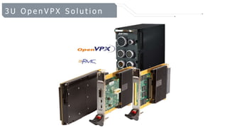
- 1. 3 U O p e n V P X S o l u t i o n
- 2. COTS Products • Legacy Altera-based PMC Products • Data Acquisition PM480, PM488 • FPGA Processing PM430,PM432 • Technology Stratix® and Stratix® II GX • Still available • New Products • VF36X 3U OpenVPX Family • VF360 Altera Stratix® V • VF361 Altera Arria® V SoC • Texas Instruments KeyStone™ DSP
- 3. VF360 Stratix® V FPGA Module with DSP & FMC - Overview • 3U OpenVPX SBC Board • PCIe Data plane • User I/O • Alterar Stratix® V FPGA • Texas Instruments Multicore DSP • KeyStone - C667X family • Front panel I/O via FMC site • Mechanics • Air- & Conduction cooled
- 4. 3U OpenVPX Profile • MOD3-PAY-3F2U-16.2.12-2 module profile • PCIe Gen2 Data plane • 3x Fat Pipes (4 Lanes) = 12 Lanes 6 Giga Byte/s (GB/s) backplane bandwidth • 2x GigE 1000BASE-BX Control plane • System Controller (PCIe Root Complex) or Payload module (PCIe end point) • User I/O • 10x High Speed Serial Lanes (5GB/s) • 24x single-ended I/O’s
- 5. Altera Stratix® V family of FPGAs • Altera's 28 nm Stratix® V FPGAs deliver high bandwidth, high level of system integration and ultimate flexibility with reduced cost for for high-end applications. • VF360 Supports various GX and GS FPGAs • KF40 (1517 FPGA) package • GX variants (Logic rich) • 5SGXA3, 5SGXA4, 5SGXA5, 5SGXA7, 5SGXA9 and 5SGXAB • GS variants (Multiplier rich) • 5SGSD4, 5SGSD5, 5SGSD6 and 5SGSD8
- 6. Stratix® V FPGA Interfaces • 8x PCIe Gen2 to Switch - (4GB/s) • 4x SRIO to DSP - (2GB/s) • 10x HSSI to FMC - (5GB/s) • 34x LVDS to FMC • TX and RX pairs • 2x 1GB DDR3 memory banks • 2x 16MB QDRII+ memory banks • 24x Single-ended I/O to VPX P2 • 10x HSSI to VPX P2 - (5GB/s)
- 7. Texas Instruments KeyStone™ Multicore DSP • Texas Instruments TMS320C667X • Supports from 1 to 8 cores @ 1.25GHz • 64-bit DDR3 running @ 1333MT/s • 16 GFLOPs per DSP core • Operating Systems • DSP #0 boots Linux kernel or DSP/BIOS™ RTOS • DSP/BIOS™ RTOS on other cores • Safety Critical RTOS options available
- 8. KeyStone™ DSP Interfaces • 2x PCIe Gen2 to Switch (1GB/s BW) • 4x SRIO to FPGA (1.25 GB/s BW) • 2x GigE 1000BASE-BX to backplane • 2GB DDR3 memory bank • 64-bit data bus • 1333MT/s
- 9. Generic Front Panel I/O via FMC • VITA 57.x FMC site (subset HPC) • 10x HSSI Lanes to/from FPGA (5GB/s) • 34 bi-directional LVDS pairs • I2C Control bus • Programmable I/O voltage (Vadj)
- 10. Mechanical Packaging • Conduction cooled – Conduction cooled chassis – Rugged systems • No Front Panel I/O – Use rear I/O • VITA 47 Class – CC2 (-40°C to 55°C) – CC3 (-40°C to 70°C) • Convection cooled – Lab development – Air-cooled systems • Front Panel I/O – Application specific FMC – Test FMC for debugging • VITA 47 Class – FC2 (-40°C to 55°C) – FC3 (-40°C to 70°C)
- 11. DSP OS & BSP • Host Operating System options (core-0) • TI Linux ‘C6x BSP version 2.0 • TI SYS/BIOS with PCIe enumeration • 3RD Party RTOS (for Safety Critical applications) • Drivers for all standard peripherals • PCIe driver for FPGA • Unified FPGA memory map for PCIe & SRIO • Utilities • FPGA configuration from RBF file / NAND • Sample application • Access FPGA DDR3 and QDRII+ memories • Scatter Gather DMA
- 12. VF361 Arria® V SoC FPGA Module with Dual core ARM, DSP & FMC • 3U OpenVPX board • PCIe Data plane • User I/O • Arria® V SoC FPGA • Dual-core ARM Cortex™-A9 • Texas Instruments Multicore DSP • C667X family • Front panel I/O via FMC site • Mechanics • Air- & Conduction cooled
- 13. Altera Arria® V SoC family of FPGAs • Altera’s Arria® V SoC • High performance 28 nm SoC FPGA with the lowest total power for midrange applications • VF361 supports SX FPGA variants • Embedded device memory: 19-25 Mb • Embedded device multipliers (18x18): 1,618 - 2,180 • Hard Processor System (HPS) • Dual-core ARM Cortex-A9 MPCore CPU • ARM NeonTM media processing engine with double precision vector floating point (FVP)
- 14. VF36X Companion Modules • VR300 Rear Transition Module • FPGA USB Blaster • Quartus Programmer • Debugging with SignalTap II • DSP XDS100 • Software debugging • Mini-SAS Interface • 4X HSSI Lanes • Ethernet (GigE) SFP Case
- 15. VF36X Companion FMC Modules • FM500 Test FMC • FPGA USB Blaster – Quartus Programmer Pod – Debugging with SignalTap II • DSP TI-XDS100 – Software debugging • Mini-SAS Interface – 4x MGT Lanes • FM550 Dual Channel SAS I/O FMC • 2x SFF-8088 interfaces – 4x lanes per interface • Compliant with mini-SAS pin-out • Designed for up to 10Gbps operation • HPC FMC Interface – 8x MGT Lanes
- 16. VF36X Companion FMC Modules • FM510 Video I/O FMC • Digital + Analogue Video – 3G-SDI input & output • General Purpose I/O – RS422 & RS485 – CAN Bus & Discrete IOs – Audio • VITA57.1 FMC HPC (no MGT required) • FMC410 Optical I/O FMC • Ten independent channels – Transmitter/Receive • Up to 10Gbps speed • VITA57.1 FMC HPC – 13.5 mm stacking height • None-standard!
- 17. VF36X Companion FMC Modules • FMC667 C6678 DSP FMC • 8-core TMS320C6678 DSP – Each core @ 1.25GHz • 1GB Local Memory – DDR3 • Gigabit Ethernet – RJ45 on Front Panel • VITA 57.1 LPC or HPC – Serial Rapid I/O on HPC • FMC407 Clocking FMC • Eight Clock Outputs – 34.375MHz-4.4GHz – 30.72MHz ref clock • Eight Triggers – 1PPS signals • GPS Receiver • VITA 57.1 LPC (no MGT required)
- 18. VF36X Companion FMC Modules • FMC211 Quad DAC FMC • TI’s DAC3484 – 1.25GHz Interpolation – 312MSPS Native – 16-bit/channel • Xilinx Artix-7 XC7A15T FPGA – Configuration Memory – Dual Bank 64Mx16 • VITA57.1 LPC (no MGT required) • FMC311 Dual DAQ FMC • TI’s ADC3244 – Dual ADC – 14-bit @ 125MSPS • ADI’s AD9747 – Dual DAC – 16-bit @ 250MSPS • Xilinx Artix-7 XC7A15T FPGA – Configuration Memory – Single Bank 64Mx16 • VITA57.1 LPC (no MGT required)
- 19. VF36X Companion FMC Modules • RFM-ADCFN10 ADC FMC • ADI’s AD9650 – Dual ADC – 16-bit @ Up to 105MSPS • 10x Channels Input – DC or AC coupled • VITA57.1 HPC (no MGT required) • RFM-DACNF08 DAC FMC • ADI’s AD9122 – Dual DAC – 16-bit @ 1200MSPS • 8x channels Output – DC or AC coupled • VITA57.1 HPC (no MGT required)
- 20. VS-330 - VPX Test Platform • Open Frame development system • One System slot and two Payload slots with Fat Pipe (FP) connections in between • 3 Rear Transition slots • 200W power supply • Air cooled fan controller • Ideally suited for software, firmware and hardware development of 3U VPX modules.
- 21. Typical Applications • Radar Signal Processing • Digital Down Conversion, Doppler filter, Pulse compression, CFAR • Spectrum analysis in EW • Signal detection & classification, jammer control • Video and image processing • Video overlay & Symbology engine • DCT, 1D/2D convolution, etc. • Software Defined Radio (SDR) • Real-time DSP functions • DDC, FFT, FIR, NCO, etc. • Mission Computers • Stores & Avionic computer • Safety Critical RTOS options available