PAC-Grenoble: Look inside your devices, non-destructive analysis
•
0 gefällt mir•449 views

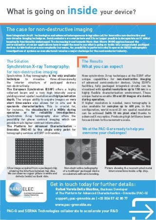
The case for non-destructive imaging New integrated circuit technologies and advanced heterogeneous integration call for innovative non-destructive and non-invasive imaging techniques. Semiconductors are everywhere and it is no longer possible to decapsulate an IC whilst keeping its functionality undamaged. The increasing trend towards More-than-Moore (MtM) approaches and the universalisation of sensor applications have brought the need to see what is going on inside fully encapsulated packaged devices. As fabrication process complexity increases, the possibility to perform in situ/in operando 3D/2D radiographic investigations of systems as manufactured remains a major challenge for the semiconductor industry.

Empfohlen
Empfohlen
Weitere ähnliche Inhalte
Kürzlich hochgeladen
Kürzlich hochgeladen (20)
Empfohlen
Empfohlen (20)
PAC-Grenoble: Look inside your devices, non-destructive analysis
- 1. Rafael Varela Della Giustina, Business Developer of The Platform for Advanced Characterisation - Grenoble (PAC-G) support pac-grenoble.eu | +33 (0)4 57 42 80 77 www.pac-grenoble.eu PAC-G and SERMA Technologies collaborate to accelerate your R&D Get in touch today for further details: P The case for non-destructive imaging New integrated circuit technologies and advanced heterogeneous integration call for innovative non-destructive and non-invasive imaging techniques. Semiconductors are everywhere and it is no longer possible to decapsulate an IC whilst keeping its functionality undamaged. The increasing trend towards More-than-Moore (MtM) approaches and the universalisation of sensor applications have brought the need to see what is going on inside fully encapsulated packaged devices. As fabrication process complexity increases, the possibility to perform in situ/in operando 3D/2D radiographic investigations of systems as manufactured remains a major challenge for the semiconductor industry. What is going on inside your device? Slice image acquired from a packaged chip showing the interface between two dies. We can observe copper pillars in white and defects (voids) as black dots. Non-destructive radiography of a multilayer packaged device on substrate with wire bonding. We at the PAC-G are ready to help you overcome your challenges! Picture showing the reconstructed metal interconnections inside a flip chip. The Results What you can expect New synchrotron X-ray techniques at the ESRF offer unique capabilities for non-destructive imaging of advanced semiconductor devices. Using ESRF’s facilities, fully packaged integrated circuits can be visualised with spatial resolutions up to 150 nm in a highly flexible characterisation environment. These unique features enable 3D and 2D images of a device during operation. If higher resolution is needed, nano tomography is also available for samples up to 400 µm. In this configuration, world record 23 nm spatial resolution can be achieved (with 10 nm pixel size) thanks to advanced X-ray optics. Produsing high brilliance beam focused down to the nanometre scale. The Solution Synchrotron X-ray Tomography: for non-destructive imaging Synchrotron X-Ray tomography is the only available technique to visualise three-dimensionally the interior structure of packaged devices non-destructively. The European Synchrotron (ESRF) offers a highly coherent beam and a very high intensity source yielding unmet spatial resolution and high penetration depth. The unique ability to acquire images on very short time-scales also allows for in situ and in operando characterisation. This is crucial for, for instance, the visualisation of a MEMs during operation or for reliability investigations. Synchrotron X-ray tomography also offers the possibility for phase contrast imaging which can provide much higher contrast information. The Platform for Advanced Characterisation - Grenoble (PAC-G) is the single entry point for tomography services at ESRF in Grenoble.
- 3. @ @