Red–green–blue light emitting diodes and distributed Bragg reflectors based on ZnCdMgSe lattice-matched to InP
•
1 gefällt mir•546 views

![M.C. Tamargo et al. / Journal of Crystal Growth 227–228 (2001) 710–716 711
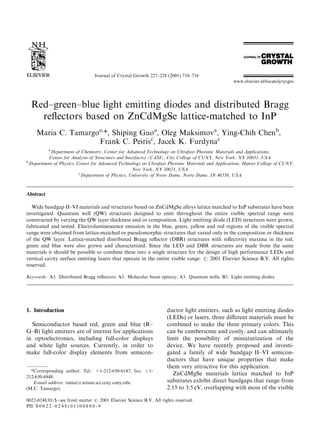
spectral range [1,2]. Fig. 1 shows the plot of the LEDs and the demonstration of monolithic (i.e.,
bandgap versus lattice constant for this family of grown on a single substrate) R–G–B structures.
materials. Instead of the actual lattice constant we We will also present results of high reflectivity
have plotted the lattice mismatch (Da=aÂ100) to distributed Bragg reflector (DBR) structures made
InP, since InP is the substrate of interest. Open from these materials that operate throughout the
circles indicate layers grown of various composi- visible range. We propose that by combining these
tions. It is clear from Fig. 1, that by combining results, novel devices, such as resonant cavity
ZnCdSe quantum well (QW) layers with LEDs and vertical cavity surface emitting lasers
ZnCdMgSe layers, lattice matched QW structures (VCSELs) may be achieved. Furthermore, because
can be made whose emission energy will vary from the R–G–B light is obtained from nearly identical
2.2 to 3.0 eV by only changing the QW thickness structures that differ only in the QW thickness
[3]. In order to reach the red emission range and/or composition, the integration of the three
(B2.0 eV), a strained ZnCdSe QW with excess Cd colors onto a single device element may be
(solid triangle in Fig. 1) can be used, whose explored.
thickness can be kept within the pseudomorphic
layer regime to avoid the formation of misfit
dislocations. Also shown in Fig. 1 is the curve for 2. Experimental procedure
the ZnSeTe alloys. Lattice-matched ZnSeTe
layers, as we will discuss below, can be highly The materials were prepared by molecular beam
doped p-type, and can serve as p-type ohmic epitaxy (MBE) using a dual chamber Riber 2300P
contacts for the device structures based on MBE system that includes a chamber for the
ZnCdMgSe materials. growth of As-based III–V materials and another
In this paper, we summarize the current status for the growth of wide bandgap II–VI compounds.
of these materials, their application as R–G–B The two chambers are connected by ultra-high
vacuum (UHV) transfer modules. Epi-ready InP
(1 0 0) substrates were mounted on 200 moly-blocks
and introduced in the MBE chamber, where they
were deoxidized in the III–V chamber under an As
flux, at 450–4801C. An InGaAs buffer layer, lattice
matched to InP, was then grown with an As-
terminated surface having a (2 Â 4) surface recon-
struction. The substrate was transferred to the II–
VI chamber, and the InGaAs surface was exposed
to a Zn flux (Zn-irradiation) for a few seconds
prior to II–VI deposition. Then a ZnCdSe inter-
facial layer was grown at low temperature (1701C)
during approximately 1 min. Growth was inter-
rupted and the temperature adjusted to the
optimum growth temperature of 250–2751C at
which point the desired ZnCdMgSe-based layer or
Fig. 1. Bandgap versus lattice constant, given as % lattice structure was grown. These steps have been
mismatch to InP, for the (Zn, Cd, Mg)Se alloy. The ternary previously used to achieve a low defect density
Zn(Se, Te) alloy relationship is also shown. Bandgap values are and high crystalline quality in these materials [4].
given at 10 K. The solid line connecting the ZnSe and CdSe and Fe-doped semi-insulating InP and n-type Si doped
the dashed line connecting the ZnSe and ZnTe binaries
InP substrates were used for test samples or device
represent measured dependences of the bandgap and lattice
constant for these ternary materials. Other ternary lines are structures, respectively. Doped ZnCdMgSe layers
assumed linear. Open circles and filled triangle represent data with n-type doping levels as high as 1018/cm3 were
points for layers grown. obtained using Chlorine as the dopant, obtained](data:image/gif;base64,R0lGODlhAQABAIAAAAAAAP///yH5BAEAAAAALAAAAAABAAEAAAIBRAA7)
Empfohlen
Empfohlen
Weitere ähnliche Inhalte
Was ist angesagt?
Was ist angesagt? (20)
Andere mochten auch
Andere mochten auch (8)
Ähnlich wie Red–green–blue light emitting diodes and distributed Bragg reflectors based on ZnCdMgSe lattice-matched to InP
Ähnlich wie Red–green–blue light emitting diodes and distributed Bragg reflectors based on ZnCdMgSe lattice-matched to InP (20)
Mehr von Oleg Maksimov
Mehr von Oleg Maksimov (20)
Kürzlich hochgeladen
Kürzlich hochgeladen (20)
Red–green–blue light emitting diodes and distributed Bragg reflectors based on ZnCdMgSe lattice-matched to InP
- 1. Journal of Crystal Growth 227–228 (2001) 710–716 Red–green–blue light emitting diodes and distributed Bragg reflectors based on ZnCdMgSe lattice-matched to InP Maria C. Tamargoa,*, Shiping Guoa, Oleg Maksimova, Ying-Chih Chenb, Frank C. Peirisc, Jacek K. Furdynac a Department of Chemistry, Center for Advanced Technology on Ultrafast Photonic Materials and Applications, Center for Analysis of Structures and Interfactes (CASI), City College of CUNY, New York, NY 10031, USA b Department of Physics, Center for Advanced Technology on Ultrafast Photonic Materials and Applications, Hunter College of CUNY, New York, NY 10021, USA c Department of Physics, University of Notre Dame, Notre Dame, IN 46556, USA Abstract Wide bandgap II–VI materials and structures based on ZnCdMgSe alloys lattice matched to InP substrates have been investigated. Quantum well (QW) structures designed to emit throughout the entire visible spectral range were constructed by varying the QW layer thickness and/or composition. Light emitting diode (LED) structures were grown, fabricated and tested. Electroluminescence emission in the blue, green, yellow and red regions of the visible spectral range were obtained from lattice-matched or pseudomorphic structures that varied only in the composition or thickness of the QW layer. Lattice-matched distributed Bragg reflector (DBR) structures with reflectivity maxima in the red, green and blue were also grown and characterized. Since the LED and DBR structures are made from the same materials it should be possible to combine these into a single structure for the design of high performance LEDs and vertical cavity surface emitting lasers that operate in the entire visible range. r 2001 Elsevier Science B.V. All rights reserved. Keywords: A3. Distributed Bragg reflectors; A3. Molecular beam epitaxy; A3. Quantum wells; B3. Light emitting diodes 1. Introduction ductor light emitters, such as light emitting diodes (LEDs) or lasers, three different materials must be Semiconductor based red, green and blue (R– combined to make the three primary colors. This G–B) light emitters are of interest for applications can be cumbersome and costly, and can ultimately in optoelectronics, including full-color displays limit the possibility of miniaturization of the and white light sources. Currently, in order to device. We have recently proposed and investi- make full-color display elements from semicon- gated a family of wide bandgap II–VI semicon- ductors that have unique properties that make them very attractive for this application. *Corresponding author. Tel.: +1-212-650-6147; fax: +1- ZnCdMgSe materials lattice matched to InP 212-650-6848. E-mail address: tamar@scisun.sci.ccny.cuny.edu substrates exhibit direct bandgaps that range from (M.C. Tamargo). 2.15 to 3.5 eV, overlapping with most of the visible 0022-0248/01/$ - see front matter r 2001 Elsevier Science B.V. All rights reserved. PII: S 0 0 2 2 - 0 2 4 8 ( 0 1 ) 0 0 8 0 8 - 9
- 2. M.C. Tamargo et al. / Journal of Crystal Growth 227–228 (2001) 710–716 711 spectral range [1,2]. Fig. 1 shows the plot of the LEDs and the demonstration of monolithic (i.e., bandgap versus lattice constant for this family of grown on a single substrate) R–G–B structures. materials. Instead of the actual lattice constant we We will also present results of high reflectivity have plotted the lattice mismatch (Da=aÂ100) to distributed Bragg reflector (DBR) structures made InP, since InP is the substrate of interest. Open from these materials that operate throughout the circles indicate layers grown of various composi- visible range. We propose that by combining these tions. It is clear from Fig. 1, that by combining results, novel devices, such as resonant cavity ZnCdSe quantum well (QW) layers with LEDs and vertical cavity surface emitting lasers ZnCdMgSe layers, lattice matched QW structures (VCSELs) may be achieved. Furthermore, because can be made whose emission energy will vary from the R–G–B light is obtained from nearly identical 2.2 to 3.0 eV by only changing the QW thickness structures that differ only in the QW thickness [3]. In order to reach the red emission range and/or composition, the integration of the three (B2.0 eV), a strained ZnCdSe QW with excess Cd colors onto a single device element may be (solid triangle in Fig. 1) can be used, whose explored. thickness can be kept within the pseudomorphic layer regime to avoid the formation of misfit dislocations. Also shown in Fig. 1 is the curve for 2. Experimental procedure the ZnSeTe alloys. Lattice-matched ZnSeTe layers, as we will discuss below, can be highly The materials were prepared by molecular beam doped p-type, and can serve as p-type ohmic epitaxy (MBE) using a dual chamber Riber 2300P contacts for the device structures based on MBE system that includes a chamber for the ZnCdMgSe materials. growth of As-based III–V materials and another In this paper, we summarize the current status for the growth of wide bandgap II–VI compounds. of these materials, their application as R–G–B The two chambers are connected by ultra-high vacuum (UHV) transfer modules. Epi-ready InP (1 0 0) substrates were mounted on 200 moly-blocks and introduced in the MBE chamber, where they were deoxidized in the III–V chamber under an As flux, at 450–4801C. An InGaAs buffer layer, lattice matched to InP, was then grown with an As- terminated surface having a (2 Â 4) surface recon- struction. The substrate was transferred to the II– VI chamber, and the InGaAs surface was exposed to a Zn flux (Zn-irradiation) for a few seconds prior to II–VI deposition. Then a ZnCdSe inter- facial layer was grown at low temperature (1701C) during approximately 1 min. Growth was inter- rupted and the temperature adjusted to the optimum growth temperature of 250–2751C at which point the desired ZnCdMgSe-based layer or Fig. 1. Bandgap versus lattice constant, given as % lattice structure was grown. These steps have been mismatch to InP, for the (Zn, Cd, Mg)Se alloy. The ternary previously used to achieve a low defect density Zn(Se, Te) alloy relationship is also shown. Bandgap values are and high crystalline quality in these materials [4]. given at 10 K. The solid line connecting the ZnSe and CdSe and Fe-doped semi-insulating InP and n-type Si doped the dashed line connecting the ZnSe and ZnTe binaries InP substrates were used for test samples or device represent measured dependences of the bandgap and lattice constant for these ternary materials. Other ternary lines are structures, respectively. Doped ZnCdMgSe layers assumed linear. Open circles and filled triangle represent data with n-type doping levels as high as 1018/cm3 were points for layers grown. obtained using Chlorine as the dopant, obtained
- 3. 712 M.C. Tamargo et al. / Journal of Crystal Growth 227–228 (2001) 710–716 from a ZnCl2 source. A Nitrogen RF-plasma source was used to introduce Nitrogen in the layers for p-type doping. The growth of ZnCdSe, ZnCdMgSe and ZnSeTe layers was done at about 1 mm per hour under group VI-rich conditions. The layers and the structures were characterized using single and double crystal X-ray diffraction, photoluminescence (PL) measurements, Hall ef- fect, capacitance–voltage (C2V) and current– voltage (I2V) measurements. Devices were fabri- cated by depositing Au dots on the top surface and attaching Au wires to the back n+InP substrate coated with In and the top Au dot. The Au dot was B0.3 mm2. No post growth annealing was performed. The surface electroluminescence (EL) spectra of the device structures under pulsed Fig. 2. Photoluminescence emission energy (at 10 K) as a operation at various current levels were measured function of quantum well (QW) thickness for three sets of using a microscope objective and focusing into an ZnCdMgSe-based QW structures. Solid circles represent near optical multi-channel analyzer to record their lattice matched Zn0.5Cd0.5Se wells, open diamonds represent spectral characteristics. The refractive index of strained Zn0.3Cd0.7Se wells, and the open triangles represent single layers of ZnCdMgSe was measured using a lattice matched quaternary Zn0.3Cd0.4Mg0.3Se wells. Dashed lines are drawn to aid the eye. prism coupler technique that has been previously reported [5]. Reflectivity spectra were measured with a Cary 500 UV-Visible Spectrophotometer with a Variable Angle Specular Reflectance necessary to use slightly strained Cd-rich accessory. The data were calibrated using an Zn0.3Cd0.7Se QW layers. Data from a set of Ag-coated mirror of known reflectivity as refer- samples with strained Zn0.3Cd0.7Se QWs are ence. shown by the open diamonds in Fig. 2. In this case, the QW layer has a bandgap of about 2.0 eV. Emission in the red range is obtained with various 3. Results and discussion QW thicknesses. To avoid the formation of misfit dislocations due to relaxation, QW thickness less The unique characteristics of these materials are ( than 50 A can be used. An additional set of best illustrated by investigating QW structures data is shown in Fig. 2 as open triangles. These made from them. The PL peak emission energy of correspond to QWs with lattice-matched three sets of samples with various QW thicknesses Zn0.3Cd0.4Mg0.3Se QW layers of bandgap of and composition are shown in Fig. 2. The mea- B2.6 eV. These quaternary QWs produce blue surements were made at 10 K. The solid circles ( emission from QW layers that are 40–50 A, rather represent the set of near-lattice-matched ( than the 20–25 A layers required for blue emission Zn0.5Cd0.5Se QWs with ZnCdMgSe barriers. The when near-lattice-matched Zn0.5Cd0.5Se QWs were bandgap energy of the barrier layer is in the range used (circles). Thicker QW layers result in nar- of B3.0 eV. The bandgap of a thick layer of rower emission lines and higher luminescence Zn0.5Cd0.5Se of the same composition as that used efficiencies from the structures, and are desirable in the QW layers was 2.27 eV. A large range of for low threshold diode lasers [6]. From these data emission energies is obtained from these structures we conclude that red–green–blue (R–G–B) emis- by changing only the QW thickness, with values sion is readily obtained from lattice-matched or corresponding to emission ranging from blue to pseudomorphic structures in which only in the QW yellow. In order to achieve red emission it is thickness and/or composition are varied. This
- 4. M.C. Tamargo et al. / Journal of Crystal Growth 227–228 (2001) 710–716 713 unique characteristic makes this set of materials emission lines at 495, 537 and 603 nm were clearly ideally suited for the fabrication of semiconductor observed. The lower PL intensity obtained from based full-color displays and white light sources. the red QW is due to the fact that many of the Furthermore, it should be possible to make carriers are captured by the blue and green QWs, monolithic three-color structures, grown on a which are closer to the surface. single substrate. We recently used shadow mask In order to fabricate devices, the material selective area epitaxy to demonstrate this possibi- quality is of utmost importance and the possibility lity [7]. To further demonstrate the potential for of bipolar doping is essential. Excellent material integration of the three-color components onto a quality has been demonstrated using the optimum single substrate we have grown a structure with growth conditions described above. Narrow X-ray three stacked QWs designed to emit one in the red, rocking curves (less than 50 arcsec full widths at one in the green and one in the blue spectral half maximum), strong and sharp PL spectra regions. The PL spectrum for this structure exhibiting only bandedge emission, and low measured at room temperature using the 325 nm stacking fault densities of 5 Â 104/cm2 are typical line from a He–Cd laser is shown in Fig. 3. The characteristics [4]. We have also demonstrated n- inset in Fig. 3 shows the schematic of the structure. type doping up to about 1 Â 1018/cm3 for quatern- The first QW grown was the red QW, which aries with bandgaps as high as 3.0 eV [8]. These consists of a strained ZnCdSe ternary layer levels are fully compatible with practical lasers and nominally 4.5 nm thick. The green and blue QWs LEDs. p-type doping of the quaternary layers has were made of near-lattice-matched ZnCdSe mate- also been achieved, but net acceptor levels are rial, nominally 2.0 and 1.0 nm thick, respectively. presently limited to 1 Â 1016/cm3 [9]. Although The wells were separated by 20 nm thick barrier these doping levels are sufficient for LED applica- layers. The top and bottom barrier layers were 500 tions, higher levels are required for injection laser and 100 nm, respectively. Barrier layers were all operation. Finally, a p+ doping level of 2 Â 1019/ ZnCdMgSe lattice-matched quaternaries with a cm3 for ZnSeTe lattice matched to InP has been bandgap of 2.9 eV. The entire structure was demonstrated [10]. This material can be used as a pseudomorphic to the InP substrate. Three sharp p-type ohmic contact for the LEDs without introducing defects due to lattice mismatch. Combining these results LED structures were fabricated from these materials. The structures consist of: (1) a quaternary ZnCdMgSe barrier (500 nm thick) layer with a bandgap of B2.9 eV doped n-type to a level of 1 Â 1018/cm3, (2) a ZnCdSe QW layer whose thickness and composi- tion were varied to achieve various electrolumines- cence (EL) emission wavelengths, (3) a p-type ZnCdMgSe barrier layer (100 nm thick) with a bandgap also B2.9 eV doped with Nitrogen to a level of B1 Â 1016/cm3, and (4) a p+ contact layer (B20 nm thick) lattice matched ZnSeTe doped with Nitrogen to B1019/cm3. Four LED structures were grown with different QW thickness and/or composition. The QW parameters used are listed in Table 1. Au contacts were deposited on the Fig. 3. Room temperature PL for a structure consisting of structures and the devices were forward biased for three stacked QWs designed to emit in the red, green and blue regions of the visible spectral range. The inset is a schematic of operation. Good I2V characteristics were ob- the structure. Details of layer thickness and compositions are served, with low operating voltages estimated at 4– discussed in the text. 5 V at typical LED current densities of 5 A/cm2.
- 5. 714 M.C. Tamargo et al. / Journal of Crystal Growth 227–228 (2001) 710–716 Table 1 Parameters for the four LED structures investigated LED Color QW QW thickness EL (RT) EL (RT) EL (RT) Da=a (%) ( (A) wavelength (nm) energy (eV) FWHM (nm) Blue o0.2 15 500 2.480 19 Green o0.2 20 520 2.385 17 Yellow o0.2 60 552 2.244 18 Red 1.2 100 630 1.967 27 This indicates good ohmic contacts and reasonable exhibit greatly reduced degradation rates com- doping levels for the materials [9]. The EL spectra pared to the degradation of blue–green LEDs are shown in Fig. 4. EL emission in the red, yellow, made from the ZnCdSe/ZnMgSSe structures on green and blue regions of the visible spectral range GaAs. The InP-based LEDs similar to the ones we were obtained. Narrow widths, with less than propose in this work did not exhibit dark-line 20 nm of full width at half maximum (FWHM), defects (DLDs), a typical defect often observed in were achieved for all but the red LED. The wider other II–VI structures. We have also observed that EL emission peak (27 nm FWHM) from the red our QW and LED structures do not form DLDs LED is believed to be due to the partially relaxed when subjected to e-beam induced degradation 10 nm thick QW used for the device structure. Use [12]. The absence of DLDs and the longer device of a pseudomorphic well (4–5 nm) should improve lifetimes suggest that the materials proposed in the EL characteristics of the red LED. Recently, this work may be less prone to degradation than Faschinger et al. [11] reported blue–green LEDs other wide bandgap II–VI materials. made from the same alloy materials and a similar The operating characteristics of the LEDs, such structure to the ones we have used. His devices as luminescence quantum efficiency, could be further improved by incorporating distributed Bragg reflector (DBR) mirrors in the device structure. Bragg mirrors may be used to reduce loss due to III–V substrate absorption, and they would also allow the design of vertical cavity surface emitting lasers (VCSELs) and resonant- cavity LEDs. For these reasons we have also grown DBR structures made from these ZnCdMgSe materials. Due to the large bandgap range available from the ZnCdMgSe layers lattice matched to InP used in our devices (see Fig. 1), a large variation of the index of refraction is expected from these materials. Recently, we have measured the refractive index, at several wave- lengths, for a set of quaternary layers ranging in bandgap from 2.2 to 2.9 eV using the prism coupler technique [13]. With these data, we have designed stacks of alternating ZnCdSe and ZnCdMgSe layers lattice matched to InP having Fig. 4. Electroluminescence spectra measured at room tem- perature for four LED structures based on lattice matched 10–16 periods. The periods were designed such ZnCdMgSe on InP, designed to emit in the red, yellow, green that the DBRs would operate in the red region. and blue regions of the visible spectral range. For operation in the blue–green, it was necessary
- 6. M.C. Tamargo et al. / Journal of Crystal Growth 227–228 (2001) 710–716 715 Table 2 Parameters of DBR structures DBRs Composition di a Eg (77 K) n Dn=n N lmax (nm) R (%) (nm) (eV) (%) DBR (a) Zn0.52Cd0.48Se/ 59.7 2.16 2.72 12 10 685 80 Zn0.30Cd0.28Mg0.42Se 68.0 2.86 2.39 DBR (b) Zn0.52Cd0.48Se/ 56.1 2.16 2.72 12 16 605 95 Zn0.30Cd0.28Mg0.42Se 63.9 2.86 2.39 DBR (c) Zn0.34Cd0.33Mg0.33Se/ 51.0 2.65 2.60 9 10 507 77 Zn0.23Cd0.18Mg0.59Se 55.8 3.10 2.37 a Nominal individual layer thickness. to use stacks of two quaternary layers, since the optical thickness of the individual layers to one- ZnCdSe low bandgap layer absorbs in that quarter of the desired stop-band wavelength wavelength range. Table 2 summarizes the para- produced DBRs with reflectivity maxima at 685, meters of three DBR structures. Their reflectivity 605 and 507 nm, in the red to blue–green range. spectra are shown in Fig. 5. Adjustment of the Reflectivity of 95% for DBR structures having 16 periods and 80% for structures with 10 periods were observed. Calculations based on the phase transfer method [14] for structures having compar- able index of refraction steps (Dn=n) to the structures grown predict that reflectivity of nearly 100% could be achieved if 25–26 periods were used. Such high reflectivity is needed for practical VCSEL design. 4. Conclusions In summary, we have investigated a set of wide bandgap II–VI materials and structures based on ZnCdMgSe alloys lattice matched to InP sub- strates. We have made QW structures in which only the QW layer thickness and/or composition was varied. These QW structures could be designed to emit throughout the entire visible spectral range. To illustrate the potential for integration of the R–G–B colors onto a single device, a pseudomorphic structure with three stacked QWs that emit in the red, green and blue regions was grown. LED structures were also grown, fabricated and tested. EL spectra in the red, yellow, green, and blue emission regions were Fig. 5. Reflectivity spectra for three lattice-matched obtained from lattice matched or pseudomorphic ZnCdMgSe-based distributed Bragg reflector (DBR) structures structures that varied only in the composition or designed to operate in the visible spectral range. thickness of the QW. Lattice matched DBR
- 7. 716 M.C. Tamargo et al. / Journal of Crystal Growth 227–228 (2001) 710–716 structures designed to operate in the red, green and [2] T. Morita, A. Kikuchi, I. Nomura, K. Kishino, J. blue were also grown and characterized. Since the Electron. Mater. 25 (1996) 425. [3] A. Cavus, L. Zeng, M.C. Tamargo, N. Bambha, F. LEDs and the DBR structures are made from the Semendy, A. Gray, Appl. Phys. Lett. 68 (1996) 3446. same materials it should be possible to combine [4] L. Zeng, S.P. Guo, Y.Y. Luo, W. Lin, M.C. Tamargo, H. these into a single structure for the design of high Xing, G.S. Cargill III, J. Vac. Sci. Technol. B 17 (1999) performance LEDs and VCSEL that operate in the 1255. entire visible range. [5] F.C. Peiris, S. Lee, V. Bindley, J.K. Furdyna, J. Appl. Phys. 84 (1998) 5194. [6] S.P. Guo, L. Zeng, M.C. Tamargo, Appl. Phys. Lett. 78 (2001) 1. Acknowledgements [7] Y. Luo, S.P. Guo, O. Maksimov, M.C. Tamargo, V. Asnin, F.H. Pollak, Y.C. Chen, Appl. Phys. Lett. 77 (2000) 4259. The authors would like to acknowledge the [8] W. Lin, A. Cavus, L. Zeng, M.C. Tamargo, J. Appl. Phys. support of the National Science Foundation 84 (1998) 1472. (NSF) through grant number ECS9707213 and [9] M.C. Tamargo, W. Lin, S.P. Guo, Y. Luo, Y. Guo, Y.C. the Army Research Laboratory through grant Chen, J. Crystal Growth 214/215 (2000) 1058. number DAAD17-99-C-0072. Two of us (FP [10] W. Lin, B.X. Yang, S.P. Guo, A. Elmoumni, F. Fernandez, M.C. Tamargo, Appl. Phys. Lett. 75 (1999) and JKF) would also like to acknowledge the 2608. support of the NSF through grant number . [11] W. Faschinger, J. Nurnberger, Appl. Phys. Lett. 77 (2000) DMR0072897. 187. [12] L.L. Chao, H. Xing, G.S. Cargill, III, L. Zeng, M.C. Tamargo, Presented at the APS March Meeting, Los Angeles, 1998. References [13] F.C. Peiris, J.K. Furdyna, S.P. Guo, M. C. Tamargo, J. Appl. Phys. 89 (2001) 3748. [1] N. Dai, A. Cavus, R. Dzakpasu, M.C. Tamargo, F. [14] O. Maksimov, S.P. Guo, L. Zeng, M.C. Tamargo, Semendy, N. Bambha, D.M. Hwang, C.Y. Chen, Appl. F.C. Peiris, J.K. Furdyna, J. Appl. Phys. 89 (2001) Phys. Lett. 66 (1995) 2742. 2202.