
Empfohlen
Weitere ähnliche Inhalte
Was ist angesagt?
Was ist angesagt? (20)
Ähnlich wie dc ac inverters
Ähnlich wie dc ac inverters (20)
Kürzlich hochgeladen
Kürzlich hochgeladen (20)
dc ac inverters
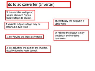
- 1. A variable output voltage may be obtained in two ways : 1. By varying the input dc voltage 2. By adjusting the gain of the inverter, usually done by PWM control. dc to ac converter (Inverter) It is a variable voltage ac source obtained from a fixed voltage dc source. Theoretically the output is a SINE wave. In real life the output is non- sinusoidal and contains harmonics.
- 2. Single phase half bridge inverter Vi t VS/2 VO t VS/2 T/2 T R Chopper VO + _ Chopper 2 V S 2 V S T/2 VS/2 dt dt T 2 T 2 s 2 T 0 2 s s m r 2 V 2 V T 1 V The output rms voltage is given by 2 V V s o
- 3. Single phase half bridge inverter VO t VS/2 T/2 T T/2 VS/2 Here we see that the output voltage wave is not a pure Sine wave. It can be represented as sum of n numbers of sine waves by Fourier’s series. t n n n sin V 2 v 5 , 3 , 1 s o ,.. 4 , 2 for , 0 vo n
- 4. Single phase half bridge inverter Vo t t n n n sin V 2 v 5 , 3 , 1 s o S 2V 3 2VS Fundamental component Third harmonics component
- 5. Single phase half bridge inverter VO t VS/2 T/2 T T/2 VS/2 t n n n sin V 2 v 5 , 3 , 1 s o For n=1, the fundamental component is s s 1 V 45 . 0 2 V 2 V t sin V 2 v s 1 the rms fundamental component is
- 6. Single phase half bridge inverter VO t VS/2 T/2 T T/2 VS/2 In the output the power due to fundamental component is the useful power. s s 1 V 45 . 0 2 V 2 V The power due to harmonic components is dissipated as heat and increases the load temperature.
- 7. Single phase half bridge inverter The quality of the inverter output is evaluated by some parameters. Harmonic Factor of nth harmonic, HFn 1 n n V V HF Total Harmonic distortion, THD 2,3 n 2 n 1 V V 1 THD Distortion Factor, DF 2,3 n 2 2 n 1 n V V 1 DF
- 8. Single phase half bridge inverter Numerical Example : The dc input voltage of a single phase half bridge rectifier is 48 volt. It is supplying power to a 2.4 resistor. Find (i) output voltage (ii) Fundamental component of output voltage (iii) output power (iv) peak and average current in each transistor (iv) peak reverse blocking voltage of each transistor (v) THD (vi) DF Given VS =48V and RL =2.4 Output voltage Vo=Vs/2=24V Output current Io=24/2.4=10A Output Power VoX Io=24X10=240W Each transistor conducts for 50% of time Transistor current = 10X0.5=5A
- 9. Single phase half bridge inverter The peak reverse blocking voltage for the transistor = 24 + 24 = 48V R Chopper VO + _ Chopper 2 V S 2 V S Fundamental component V1 = 0.45 X 48=21.6V rms harmonic voltage 10.46V 21.6 24 V V 2 2 2 1 2 o
- 10. R VS VO t V Q1 Q2 Q3 Q4 VB t Q3 and Q4 Single phase bridge inverter VB t Q1 and Q2 Vi t VS H Bridge
- 11. Single phase bridge inverter Vi t VS VO t VS T/2 T T/2 VS dt dt T 2 T 2 s 2 T 0 2 s s m r V V T 1 V The output rms voltage is given by s o V V Students must do the integration in detail and find the result
- 12. VS VO t V Q1 Q2 Q3 Q4 VB t Q3 and Q4 Single phase bridge inverter VB t Q1 and Q2 Vi t VS Inductive Load RL IL t IL
- 13. Single phase bridge inverter Vi t VS VO t VS T/2 T T/2 VS The frequency of the output voltage is given by T 1 f Frequency can be chosen from the time period of the base signal
- 14. Single phase bridge inverter Vi t VS VO t VS T/2 T T/2 VS s o V V Control of output voltage Single pulse width modulation Multiple pulse width modulation Sinusoidal pulse width modulation Modified Sinusoidal pulse width modulation Phase displacement control
- 15. Single phase bridge inverter Vi t VS Control of output voltage Single pulse width modulation VO t V VB t Q3 and Q4 VB t Q1 and Q2 VO t Vs VB t VB t Q1 and Q2 Q3 and Q4 (-)/2 0 2 The rms output voltage dt dt 2 3 2 3 2 s 2 2 2 s s m r V V 2 1 V S s m r V V The output voltage can be controlled by controlling the value of
- 16. Single phase bridge inverter Vi t VS Control of output voltage Multiple pulse width modulation VO t Vs VB t VB t 0 2 p V V S s m r Is the width of single pulse p Is the number of pulses per half cycle and p both can be adjusted to control the output voltage
- 17. Single phase bridge inverter Vi t VS VO t VB t VB t 0 2 Q1 and Q2 Q3 and Q4 3 , 2 , 1 S s m r V V m m The duration of individual pulse can be adjusted to different desired values, so that the lower order harmonics are eliminated and a pure/near sine wave could be obtained
- 18. Modified PWM inververter VO t VB t 10ms 10ms 50Hz f Suppose Carrier frequency =20kHz No of pulses per 10ms = 200 VB t VB t All the pulses are present 11111111 Alternate pulses are present 1010101010 pulses at desired pattern 1011011101101 Keep on trying with different patterns of pulses until a (i)sine wave of desired (ii)frequency and (iii)voltage magnitude is obtained.
- 19. Push-Pull inverter Q1 Q2 Q1 t Q2 t VB Output Easy design Near sine wave t VO Low TUF Transformer saturation Low frequency operation
- 21. Three phase inverter Q1 Q2 Q3 Q4 Primary A Primary B Primary C Q5 Q6 Q7 Q8 Q9 Q10 Q11 Q12
- 22. Three phase inverter firing sequence 0 1800 3600 T t t t t t t VB t Q3 and Q4 1200 1200 Q5 and Q6 Q9 and Q10 Q7 and Q8 Q11 and Q12 Q11 and Q12 600 Q1 and Q2 Sequence : Q1 and Q2 Q11 and Q12 Q5 and Q6 Q3 and Q4 Q9 and Q10 Q7 and Q8
- 23. Three phase inverter output voltage Primary side 0 1800 3600 T t t t VP t Phase A Phase B Phase C 1200 1200