SlideShare ist ein Scribd-Unternehmen logo
1 von 6
Downloaden Sie, um offline zu lesen
CTU: EE 395 – Electronics 2: Lab 2: Multi-stage Amplifier Design                                                                   1


                                      Colorado Technical University
                                         EE 395 – Electronics 2
                                          Lab 2: BJT Circuits
                                               May 2010
                                   Loren Schwappach, Taylor DeIaco, Victor Arosemena

          ABSTRACT: This lab report was completed as a course requirement to obtain full course credit in EE395, Electronics 2 at
Colorado Technical University. This lab report examines two multi-stage BJT circuits (Cascade and Cascode) and how they operate.
The objective of this lab is to analyze, simulate, experiment, and document the characteristics of the multi-stage amplifiers. Hand
calculations are developed using the properties of the BJTs (with B assumed at 120, and VBE on = .7V), circuit construction and then
verified using P-Spice schematic calculations to determine the viability of design prior to the physical build of the design. P-Spice
simulation results and hand calculations are then verified by physically modeling the design on a bread board and taking
measurements for observation.


                      I. INTRODUCTION

         T    HE NPN Bipolar Junction Transistor is an active
              circuit device with several uses such as signal
amplification. The DC biasing (B value of the transistor) is
used to find the linear operating region of the device and its
performance distinctiveness. The BJT transistor structure
contains three regions; the collector, base, and emitter. The
objective of this lab is to gain an understanding of how
multistage amplifiers assist in providing gain with increased
bias stability. Two specific multistage configurations are
examined, Cascade, and Cascode.


                      II. OBJECTIVES                                      Figure 1: Circuit 1: Cascade Multi-Stage Circuit
         The objective of this lab is to gain an understanding
of the physical structure, operation, and characteristics of the
multi-stage bipolar junction transistor (BJT) circuits. In
particular what the differences are between the analysis,
simulation and actual experiment results. And to recognize the
three modes of operation: saturation, active and cutoff. The
goal of this lab is to become familiar and understand how
multi-stage BJTs operate.


             III. MULTI-STAGE AMPLIFIERS
          In this lab our group designed and analyzed two
specific multi-stage amplifier circuits using the 2N3904 NPN
BJT, and the 2N3905 PNP BJT. Our first circuit was a multi-
stage cascade design consisting of a Common-emitter circuit
using a NPN transistor feeding into another Common-emitter
circuit with an PNP transistor (figure 1), our second circuit
was a multi-stage cascode design using two NPN transistors
with a trans-conductance amplifier followed by a current
buffer (figure 2).

                                                                    Figure 2: Circuit 2: Cascode Multi-Stage Amplifier Circuit
CTU: EE 395 – Electronics 2: Lab 2: Multi-stage Amplifier Design                                                                   2

           IV. DESIGN APPROACHES/TRADE-OFFS
         The performance of this lab will depend on how well
the circuits are developed. If the circuit is developed correctly
the results showed should be similar to the hand calculation
and PSpice simulation results. PSpice will be used to provide
a rough estimate of what should be expected in the circuit
measurements; however, the PSpice model transistor B tends
to vary by the model, so the PSpice simulations could have a
much larger error margin than the expected. The performance
of the lab also depends on how well the equipment is
calibrated and accurate the components tolerance is.
         This is not a very cost effective lab except for the
development and time it took to construct the lab components.
But to save money for a lab project, whether it’s the testing or
developing phase of a new design, depending on what the
schematic is, a circuit can be reduced, if done correctly.


                V.       HAND CALCULATIONS
        The scanned hand calculations used for this lab can
be found below.


                                                                    Figure 4: Circuit 2, Cascode Amplifier Hand Calculations.


                                                                                    VI.      CIRCUIT SCHEMATICS
                                                                              The final circuit schematics below were built in
                                                                    PSpice and allowed our team to analyze the circuit digitally
                                                                    before performing the physical build. However, since the B
                                                                    value of the transistor used is rarely the exact B of the
                                                                    transistor there is a margin of percentage error attributed.


Figure 3: Circuit 1, Cascade Amplifier hand calculations.


                                                                         Figure 5: Circuit 1: Cascade Amplifier Voltages
CTU: EE 395 – Electronics 2: Lab 2: Multi-stage Amplifier Design                                                               3


     Figure 6: Circuit 1: Cascade Amplifier Currents


                                                                   Figure 9: Circuit 2: Cascode Amplifier Currents


      Figure 7: Circuit 1: Cascade Amplifier Power


                                                                   Figure 10: Circuit 2: Cascode Amplifier Power

                                                                       In this lab we were also asked to find the frequency
                                                             response and gain of the cascade and cascode multi-stage
                                                             amplifier circuits. The PSpice results for both circuit designs
                                                             follows..

     Figure 8: Circuit 2: Cascode Amplifier Voltages
CTU: EE 395 – Electronics 2: Lab 2: Multi-stage Amplifier Design                                                             4


 Figure 11: Circuit 1: Cascade Amplifier Bode Plot. Note
 lower (high pass) corner frequency is 2.4 Hz, higher (low
 pass) corner frequency is 1.25 MHz. Center frequency is
        1.59 kHz which is what was used in this lab.
                                                              Figure 13: Circuit 1: Cascade Amplifier Bode Plot. Note
                                                                 Stage 1 gain is 5.16, Stage 2 is 1.82, total gain is 9.4.


 Figure 12: Circuit 2: Cascode Amplifier Bode Plot. Note
  lower (high pass) corner frequency is 4 Hz, higher (low
  pass) corner frequency is 25 MHz. Center frequency is
        12.6 kHz which is what was used in this lab.
                                                              Figure 14: Circuit 2: Cascode Amplifier Bode Plot. Note
                                                                                     gain is 5.42.
CTU: EE 395 – Electronics 2: Lab 2: Multi-stage Amplifier Design                                                                  5

                     VII. COMPONENT LIST                                                Hand
  The following is a list of components that were used in                               Calculated Pspice             Actual
constructing the BJT switch / inverter. Component values                                Results    Results            Results
were selected by the professor.                                            Vcc          10 V             10 V         10.02 V
                                                                           Vb1          2.17 V           2.063 V      2.086 V
            A digital multimeter for measuring circuit
             voltages, resistor resistances, and capacitor                 Vb2          1.09 V           1.007 V      1.023 V
             capacitance.                                                  Ve2          390 mV           354.1 mV 363 mV
            A power supply capable of delivering a constant               Vc2          1.47 V           1.411 V      1.426 V
             Vcc = 10V.                                                    Vce2         1.08 V           1.057 V      1.063 V
            Two 2N3904 NPN Transistor
                                                                           Vc1          5.47 V           5.877 V      5.898 V
             One 2N3905 PNP Transistor
            Applicable resisters for both multi-stage designs of          Vce1         4V               4.466 V      4.472 V
             values approx 82k, 10k*2, 6.8k*3, 1.82k, 1.2k,                Ib1          6 uA             4.669 uA     4.6 uA
             72k, 575.                                                     Ic1          666 uA           621.9 uA     621.9 uA
            Bread board with wires.
                                                                           Ie1          672 uA           626.5 uA     626.5 uA
            NOTE: Resistors can normally provide around +/-
             5%-25% difference between actual and designed                 Ib2          4 uA             4.8 uA       4.8 uA
             values while Capacitors generally provide around              Ic2          672 uA           626.5 uA     626.5 uA
             20%-50% difference between actual and designed                Ie2          678 uA           631.3 uA     631.3 uA
             values. You can add resisters in series as (R1+R2)
             to closer approximate required resistance values       Table 2: Circuit 2: Cascode Circuit: Comparison of Hand
             and you can add Capacitors in parallel as (C1+C2)        Calculated, PSpice, and Measured Values. Notice all
             to closely approximate required capacitance.                              values are very close.

                                                                    This lab also asked for an analysis of the actual gain vs.
                  VIII. EXPERIMENTAL DATA                           PSpice predicted. Results follow..
          The following table illustrates the measurements
taken at each stage of the lab.                                                                Pspice       Actual
                                                                                               Results      Results
                     Hand                                                         At Q1c       5.1647       4.88
                     Calculated Pspice        Actual
                                                                     Cascade At Q2c            1.8195       1.85
                     Results    Results       Results
                                                                                  Total Gain 9.397          9
       Vcc           10 V         10 V        10.02 V
                                                                                  At Q1c       5.41955      5
       Vb1           1.087 V      1.062 V     1.058 V                Cascode
                                                                                  Total Gain 5.41955        5
       Ve1           387 mV       425.4 mV 418 mV
       Vce1          7.437 V      7.2156 V    7.22 V                             IX. ANALYSIS/DATA COMPARISON
       Vc1           7.824 V      7.641 V     7.638 V
       Vce2          3.064 V      2.18 V      2.185 V                        The analysis/PSpice/Experimental data results were
       Ve2           8.524 V      8.342 V     8.35 V                all accurate, but the results differed between the three. The
                                                                    reasons that the results were different is because the
       Vc2           5.46 V       6.162 V     6.165 V               experimental results have equipment calibrations, component
       Ib1           3 uA         2.838 uA    2.6 uA                tolerances, and actual measures values from the components.
       Ic1           320 uA       351.7 uA    347 uA                The PSpice were less accurate than hand calculation because
                                                                    the PSpice B. All three results were not in total agreement
       Ie1           323 uA       354.5 uA    350 uA
                                                                    however, the results were close to each other.
       Ib2           7 uA         -4.697 uA -6 uA
       Ic2           803 uA       906.2 uA    901 uA                                       X. CONCLUSIONS
      Ie2         810 uA       910.9 uA 907 uA                               The discrepancies between the actual results, hand
Table 1: Circuit 1: Cascade Circuit: Comparison of Hand             calculated and simulated result is that they were all extremely
  Calculated, PSpice, and Measured Values. Notice all               close (<20%) from the P-Spice results, however these results
                   values are very close.                           could differ depending upon the error provided by the passive
                                                                    and active components, factors such as component tolerances,
                                                                    equipment calibrations and measurements fluctuations by the
                                                                    observer can contribute to results being slightly off from the
CTU: EE 395 – Electronics 2: Lab 2: Multi-stage Amplifier Design                6

P-Spice calculations. It is always good to start with P-Spice to
understand what is happening prior to build, and even more
important to know the characteristics (B value) of the
transistor.
          In conclusion, this lab was a great demonstration on
the powerful features of multistage BJTs and their use in
electronics.

                              REFERENCES
[1]   D. A. Neamen, “Microelectronics: circuit analysis and design - 3rd ed.”
      McGraw-Hill, New York, NY, 2007. pp. 1-107.

Weitere Àhnliche Inhalte

Was ist angesagt?

Experiment no 2 setb118
Experiment no 2    setb118Experiment no 2    setb118
Experiment no 2 setb118Omkar Rane
 
Electronic circuit design lab manual
Electronic circuit design lab manualElectronic circuit design lab manual
Electronic circuit design lab manualawais ahmad
 
Gopi 1 lab manual
Gopi 1 lab manualGopi 1 lab manual
Gopi 1 lab manualGopinath Naidu
 
Regions of operation of bjt and mosfet
Regions of operation of bjt and mosfetRegions of operation of bjt and mosfet
Regions of operation of bjt and mosfetMahoneyKadir
 
A New Instrumentation AmpliïŹer Architecture Based on Differential Difference ...
A New Instrumentation AmpliïŹer Architecture Based on Differential Difference ...A New Instrumentation AmpliïŹer Architecture Based on Differential Difference ...
A New Instrumentation AmpliïŹer Architecture Based on Differential Difference ...IJECEIAES
 
Ch4 lecture slides Chenming Hu Device for IC
Ch4 lecture slides Chenming Hu Device for ICCh4 lecture slides Chenming Hu Device for IC
Ch4 lecture slides Chenming Hu Device for ICChenming Hu
 
Loren k. schwappach ee331 - lab 3
Loren k. schwappach   ee331 - lab 3Loren k. schwappach   ee331 - lab 3
Loren k. schwappach ee331 - lab 3Loren Schwappach
 
Analog & Digital Integrated Circuits - Material (Short Answers)
Analog & Digital Integrated Circuits -  Material (Short Answers) Analog & Digital Integrated Circuits -  Material (Short Answers)
Analog & Digital Integrated Circuits - Material (Short Answers) Mathankumar S
 
Gq3112761281
Gq3112761281Gq3112761281
Gq3112761281IJERA Editor
 
Rec101 unit ii (part 2) bjt biasing and re model
Rec101 unit ii (part 2) bjt biasing and re modelRec101 unit ii (part 2) bjt biasing and re model
Rec101 unit ii (part 2) bjt biasing and re modelDr Naim R Kidwai
 
Chapter3
Chapter3Chapter3
Chapter3vidhya DS
 
Design of oscillators using cmos ota
Design of oscillators using cmos otaDesign of oscillators using cmos ota
Design of oscillators using cmos otaRamesh Patriotic
 
Analog communications lab
Analog communications labAnalog communications lab
Analog communications labVishal kakade
 
Amplifier frequency response (part 2)
Amplifier frequency response (part 2)Amplifier frequency response (part 2)
Amplifier frequency response (part 2)Jamil Ahmed
 

Was ist angesagt? (18)

Experiment no 2 setb118
Experiment no 2    setb118Experiment no 2    setb118
Experiment no 2 setb118
 
Ec ii lab manual
Ec ii lab manualEc ii lab manual
Ec ii lab manual
 
Electronic circuit design lab manual
Electronic circuit design lab manualElectronic circuit design lab manual
Electronic circuit design lab manual
 
Gopi 1 lab manual
Gopi 1 lab manualGopi 1 lab manual
Gopi 1 lab manual
 
Regions of operation of bjt and mosfet
Regions of operation of bjt and mosfetRegions of operation of bjt and mosfet
Regions of operation of bjt and mosfet
 
A New Instrumentation AmpliïŹer Architecture Based on Differential Difference ...
A New Instrumentation AmpliïŹer Architecture Based on Differential Difference ...A New Instrumentation AmpliïŹer Architecture Based on Differential Difference ...
A New Instrumentation AmpliïŹer Architecture Based on Differential Difference ...
 
75
7575
75
 
Ch4 lecture slides Chenming Hu Device for IC
Ch4 lecture slides Chenming Hu Device for ICCh4 lecture slides Chenming Hu Device for IC
Ch4 lecture slides Chenming Hu Device for IC
 
Loren k. schwappach ee331 - lab 3
Loren k. schwappach   ee331 - lab 3Loren k. schwappach   ee331 - lab 3
Loren k. schwappach ee331 - lab 3
 
Analog & Digital Integrated Circuits - Material (Short Answers)
Analog & Digital Integrated Circuits -  Material (Short Answers) Analog & Digital Integrated Circuits -  Material (Short Answers)
Analog & Digital Integrated Circuits - Material (Short Answers)
 
84
8484
84
 
Gq3112761281
Gq3112761281Gq3112761281
Gq3112761281
 
Ee6503(r 13) qb-2013_regulation
Ee6503(r 13) qb-2013_regulationEe6503(r 13) qb-2013_regulation
Ee6503(r 13) qb-2013_regulation
 
Rec101 unit ii (part 2) bjt biasing and re model
Rec101 unit ii (part 2) bjt biasing and re modelRec101 unit ii (part 2) bjt biasing and re model
Rec101 unit ii (part 2) bjt biasing and re model
 
Chapter3
Chapter3Chapter3
Chapter3
 
Design of oscillators using cmos ota
Design of oscillators using cmos otaDesign of oscillators using cmos ota
Design of oscillators using cmos ota
 
Analog communications lab
Analog communications labAnalog communications lab
Analog communications lab
 
Amplifier frequency response (part 2)
Amplifier frequency response (part 2)Amplifier frequency response (part 2)
Amplifier frequency response (part 2)
 

Ähnlich wie Ee395 lab 2 - loren - victor - taylor

EC 2 lab manual with circulits
EC 2 lab manual with circulitsEC 2 lab manual with circulits
EC 2 lab manual with circulitsMurugan Dhandapani
 
4 ee414 - adv electroncs - lab 3 - loren schwappach
4   ee414 - adv electroncs - lab 3 - loren schwappach4   ee414 - adv electroncs - lab 3 - loren schwappach
4 ee414 - adv electroncs - lab 3 - loren schwappachLoren Schwappach
 
Single stage bjt amplifier. experiment 6
Single stage bjt amplifier. experiment 6Single stage bjt amplifier. experiment 6
Single stage bjt amplifier. experiment 6Karimi LordRamza
 
EE375 Electronics 1: lab 3
EE375   Electronics 1: lab 3EE375   Electronics 1: lab 3
EE375 Electronics 1: lab 3Loren Schwappach
 
Analog and Digital Electronics Lab Manual
Analog and Digital Electronics Lab ManualAnalog and Digital Electronics Lab Manual
Analog and Digital Electronics Lab ManualChirag Shetty
 
3 ee414 - adv electroncs - lab 2 - loren schwappach
3   ee414 - adv electroncs - lab 2 - loren schwappach3   ee414 - adv electroncs - lab 2 - loren schwappach
3 ee414 - adv electroncs - lab 2 - loren schwappachLoren Schwappach
 
Selection of Passive Component for Cockroft Walton Voltage Multiplier: A Low ...
Selection of Passive Component for Cockroft Walton Voltage Multiplier: A Low ...Selection of Passive Component for Cockroft Walton Voltage Multiplier: A Low ...
Selection of Passive Component for Cockroft Walton Voltage Multiplier: A Low ...IRJET Journal
 
Assignment 1 Description Marks out of Wtg() Due date .docx
Assignment 1  Description Marks out of Wtg() Due date .docxAssignment 1  Description Marks out of Wtg() Due date .docx
Assignment 1 Description Marks out of Wtg() Due date .docxfredharris32
 
Electrical Circuit Lab
Electrical Circuit LabElectrical Circuit Lab
Electrical Circuit LabCyber4Tech
 
ADC LAB MANUAL.docx
ADC LAB MANUAL.docxADC LAB MANUAL.docx
ADC LAB MANUAL.docxSubbuMurugan1
 
Project_Kaveh & Mohammad
Project_Kaveh & MohammadProject_Kaveh & Mohammad
Project_Kaveh & MohammadKaveh Dehno
 
Mini Project 2 - Wien Bridge Oscillator
Mini Project 2 - Wien Bridge OscillatorMini Project 2 - Wien Bridge Oscillator
Mini Project 2 - Wien Bridge OscillatorAIMST University
 
Sinusoidal Response of RC & RL Circuits
Sinusoidal Response of RC & RL CircuitsSinusoidal Response of RC & RL Circuits
Sinusoidal Response of RC & RL CircuitsSachin Mehta
 
EN1072 Laboratory.docx
EN1072 Laboratory.docxEN1072 Laboratory.docx
EN1072 Laboratory.docx4934bk
 
Hands-On Electronics.pdf
Hands-On Electronics.pdfHands-On Electronics.pdf
Hands-On Electronics.pdfivan ion
 
Ece 523 project – fully differential two stage telescopic op amp
Ece 523 project – fully differential two stage telescopic op ampEce 523 project – fully differential two stage telescopic op amp
Ece 523 project – fully differential two stage telescopic op ampKarthik Rathinavel
 

Ähnlich wie Ee395 lab 2 - loren - victor - taylor (20)

EC 2 lab manual with circulits
EC 2 lab manual with circulitsEC 2 lab manual with circulits
EC 2 lab manual with circulits
 
4 ee414 - adv electroncs - lab 3 - loren schwappach
4   ee414 - adv electroncs - lab 3 - loren schwappach4   ee414 - adv electroncs - lab 3 - loren schwappach
4 ee414 - adv electroncs - lab 3 - loren schwappach
 
Single stage bjt amplifier. experiment 6
Single stage bjt amplifier. experiment 6Single stage bjt amplifier. experiment 6
Single stage bjt amplifier. experiment 6
 
EE375 Electronics 1: lab 3
EE375   Electronics 1: lab 3EE375   Electronics 1: lab 3
EE375 Electronics 1: lab 3
 
Power Electronics lab manual BE EEE
Power Electronics lab manual BE EEEPower Electronics lab manual BE EEE
Power Electronics lab manual BE EEE
 
Analog and Digital Electronics Lab Manual
Analog and Digital Electronics Lab ManualAnalog and Digital Electronics Lab Manual
Analog and Digital Electronics Lab Manual
 
3 ee414 - adv electroncs - lab 2 - loren schwappach
3   ee414 - adv electroncs - lab 2 - loren schwappach3   ee414 - adv electroncs - lab 2 - loren schwappach
3 ee414 - adv electroncs - lab 2 - loren schwappach
 
Selection of Passive Component for Cockroft Walton Voltage Multiplier: A Low ...
Selection of Passive Component for Cockroft Walton Voltage Multiplier: A Low ...Selection of Passive Component for Cockroft Walton Voltage Multiplier: A Low ...
Selection of Passive Component for Cockroft Walton Voltage Multiplier: A Low ...
 
Assignment 1 Description Marks out of Wtg() Due date .docx
Assignment 1  Description Marks out of Wtg() Due date .docxAssignment 1  Description Marks out of Wtg() Due date .docx
Assignment 1 Description Marks out of Wtg() Due date .docx
 
Electrical Circuit Lab
Electrical Circuit LabElectrical Circuit Lab
Electrical Circuit Lab
 
Pdc lab manualnew
Pdc lab manualnewPdc lab manualnew
Pdc lab manualnew
 
ADC LAB MANUAL.docx
ADC LAB MANUAL.docxADC LAB MANUAL.docx
ADC LAB MANUAL.docx
 
Project_Kaveh & Mohammad
Project_Kaveh & MohammadProject_Kaveh & Mohammad
Project_Kaveh & Mohammad
 
Ece
EceEce
Ece
 
Mini Project 2 - Wien Bridge Oscillator
Mini Project 2 - Wien Bridge OscillatorMini Project 2 - Wien Bridge Oscillator
Mini Project 2 - Wien Bridge Oscillator
 
Sinusoidal Response of RC & RL Circuits
Sinusoidal Response of RC & RL CircuitsSinusoidal Response of RC & RL Circuits
Sinusoidal Response of RC & RL Circuits
 
EN1072 Laboratory.docx
EN1072 Laboratory.docxEN1072 Laboratory.docx
EN1072 Laboratory.docx
 
506 267-276
506 267-276506 267-276
506 267-276
 
Hands-On Electronics.pdf
Hands-On Electronics.pdfHands-On Electronics.pdf
Hands-On Electronics.pdf
 
Ece 523 project – fully differential two stage telescopic op amp
Ece 523 project – fully differential two stage telescopic op ampEce 523 project – fully differential two stage telescopic op amp
Ece 523 project – fully differential two stage telescopic op amp
 

Mehr von Loren Schwappach

Ubuntu OS Presentation
Ubuntu OS PresentationUbuntu OS Presentation
Ubuntu OS PresentationLoren Schwappach
 
EE312 Embedded Microcontrollers Lab
EE312 Embedded Microcontrollers LabEE312 Embedded Microcontrollers Lab
EE312 Embedded Microcontrollers LabLoren Schwappach
 
Ee325 cmos design lab 7 report - loren k schwappach
Ee325 cmos design   lab 7 report - loren k schwappachEe325 cmos design   lab 7 report - loren k schwappach
Ee325 cmos design lab 7 report - loren k schwappachLoren Schwappach
 
Ee325 cmos design lab 6 report - loren k schwappach
Ee325 cmos design   lab 6 report - loren k schwappachEe325 cmos design   lab 6 report - loren k schwappach
Ee325 cmos design lab 6 report - loren k schwappachLoren Schwappach
 
Ee325 cmos design lab 5 report - loren k schwappach
Ee325 cmos design   lab 5 report - loren k schwappachEe325 cmos design   lab 5 report - loren k schwappach
Ee325 cmos design lab 5 report - loren k schwappachLoren Schwappach
 
Ee325 cmos design lab 4 report - loren k schwappach
Ee325 cmos design   lab 4 report - loren k schwappachEe325 cmos design   lab 4 report - loren k schwappach
Ee325 cmos design lab 4 report - loren k schwappachLoren Schwappach
 
Ee325 cmos design lab 3 report - loren k schwappach
Ee325 cmos design   lab 3 report - loren k schwappachEe325 cmos design   lab 3 report - loren k schwappach
Ee325 cmos design lab 3 report - loren k schwappachLoren Schwappach
 
Loren k. schwappach ee331 - lab 4
Loren k. schwappach   ee331 - lab 4Loren k. schwappach   ee331 - lab 4
Loren k. schwappach ee331 - lab 4Loren Schwappach
 
Ee343 signals and systems - lab 2 - loren schwappach
Ee343   signals and systems - lab 2 - loren schwappachEe343   signals and systems - lab 2 - loren schwappach
Ee343 signals and systems - lab 2 - loren schwappachLoren Schwappach
 
Ee343 signals and systems - lab 1 - loren schwappach
Ee343   signals and systems - lab 1 - loren schwappachEe343   signals and systems - lab 1 - loren schwappach
Ee343 signals and systems - lab 1 - loren schwappachLoren Schwappach
 
Ee 352 lab 1 (tutorial) - schwappach - 15 oct 09
Ee 352   lab 1 (tutorial) - schwappach - 15 oct 09Ee 352   lab 1 (tutorial) - schwappach - 15 oct 09
Ee 352 lab 1 (tutorial) - schwappach - 15 oct 09Loren Schwappach
 
EE375 Electronics 1: lab 1
EE375   Electronics 1: lab 1EE375   Electronics 1: lab 1
EE375 Electronics 1: lab 1Loren Schwappach
 
Ee395 lab 1 - bjt - loren - victor - taylor
Ee395   lab 1 - bjt - loren - victor - taylorEe395   lab 1 - bjt - loren - victor - taylor
Ee395 lab 1 - bjt - loren - victor - taylorLoren Schwappach
 
5 ee415 - adv electronics - presentation - schwappach
5   ee415 - adv electronics - presentation - schwappach5   ee415 - adv electronics - presentation - schwappach
5 ee415 - adv electronics - presentation - schwappachLoren Schwappach
 
2 ee414 - adv electroncs - lab 1 - loren schwappach
2   ee414 - adv electroncs - lab 1 - loren schwappach2   ee414 - adv electroncs - lab 1 - loren schwappach
2 ee414 - adv electroncs - lab 1 - loren schwappachLoren Schwappach
 
Ee443 phase locked loop - presentation - schwappach and brandy
Ee443   phase locked loop - presentation - schwappach and brandyEe443   phase locked loop - presentation - schwappach and brandy
Ee443 phase locked loop - presentation - schwappach and brandyLoren Schwappach
 
Ee443 phase locked loop - paper - schwappach and brandy
Ee443   phase locked loop - paper - schwappach and brandyEe443   phase locked loop - paper - schwappach and brandy
Ee443 phase locked loop - paper - schwappach and brandyLoren Schwappach
 
EE443 - Communications 1 - Lab 3 - Loren Schwappach.pdf
EE443 - Communications 1 - Lab 3 - Loren Schwappach.pdfEE443 - Communications 1 - Lab 3 - Loren Schwappach.pdf
EE443 - Communications 1 - Lab 3 - Loren Schwappach.pdfLoren Schwappach
 
Ee443 communications 1 - lab 2 - loren schwappach
Ee443   communications 1 - lab 2 - loren schwappachEe443   communications 1 - lab 2 - loren schwappach
Ee443 communications 1 - lab 2 - loren schwappachLoren Schwappach
 
EE443 - Communications 1 - Lab 1 - Loren Schwappach.pdf
EE443 - Communications 1 - Lab 1 - Loren Schwappach.pdf EE443 - Communications 1 - Lab 1 - Loren Schwappach.pdf
EE443 - Communications 1 - Lab 1 - Loren Schwappach.pdf Loren Schwappach
 

Mehr von Loren Schwappach (20)

Ubuntu OS Presentation
Ubuntu OS PresentationUbuntu OS Presentation
Ubuntu OS Presentation
 
EE312 Embedded Microcontrollers Lab
EE312 Embedded Microcontrollers LabEE312 Embedded Microcontrollers Lab
EE312 Embedded Microcontrollers Lab
 
Ee325 cmos design lab 7 report - loren k schwappach
Ee325 cmos design   lab 7 report - loren k schwappachEe325 cmos design   lab 7 report - loren k schwappach
Ee325 cmos design lab 7 report - loren k schwappach
 
Ee325 cmos design lab 6 report - loren k schwappach
Ee325 cmos design   lab 6 report - loren k schwappachEe325 cmos design   lab 6 report - loren k schwappach
Ee325 cmos design lab 6 report - loren k schwappach
 
Ee325 cmos design lab 5 report - loren k schwappach
Ee325 cmos design   lab 5 report - loren k schwappachEe325 cmos design   lab 5 report - loren k schwappach
Ee325 cmos design lab 5 report - loren k schwappach
 
Ee325 cmos design lab 4 report - loren k schwappach
Ee325 cmos design   lab 4 report - loren k schwappachEe325 cmos design   lab 4 report - loren k schwappach
Ee325 cmos design lab 4 report - loren k schwappach
 
Ee325 cmos design lab 3 report - loren k schwappach
Ee325 cmos design   lab 3 report - loren k schwappachEe325 cmos design   lab 3 report - loren k schwappach
Ee325 cmos design lab 3 report - loren k schwappach
 
Loren k. schwappach ee331 - lab 4
Loren k. schwappach   ee331 - lab 4Loren k. schwappach   ee331 - lab 4
Loren k. schwappach ee331 - lab 4
 
Ee343 signals and systems - lab 2 - loren schwappach
Ee343   signals and systems - lab 2 - loren schwappachEe343   signals and systems - lab 2 - loren schwappach
Ee343 signals and systems - lab 2 - loren schwappach
 
Ee343 signals and systems - lab 1 - loren schwappach
Ee343   signals and systems - lab 1 - loren schwappachEe343   signals and systems - lab 1 - loren schwappach
Ee343 signals and systems - lab 1 - loren schwappach
 
Ee 352 lab 1 (tutorial) - schwappach - 15 oct 09
Ee 352   lab 1 (tutorial) - schwappach - 15 oct 09Ee 352   lab 1 (tutorial) - schwappach - 15 oct 09
Ee 352 lab 1 (tutorial) - schwappach - 15 oct 09
 
EE375 Electronics 1: lab 1
EE375   Electronics 1: lab 1EE375   Electronics 1: lab 1
EE375 Electronics 1: lab 1
 
Ee395 lab 1 - bjt - loren - victor - taylor
Ee395   lab 1 - bjt - loren - victor - taylorEe395   lab 1 - bjt - loren - victor - taylor
Ee395 lab 1 - bjt - loren - victor - taylor
 
5 ee415 - adv electronics - presentation - schwappach
5   ee415 - adv electronics - presentation - schwappach5   ee415 - adv electronics - presentation - schwappach
5 ee415 - adv electronics - presentation - schwappach
 
2 ee414 - adv electroncs - lab 1 - loren schwappach
2   ee414 - adv electroncs - lab 1 - loren schwappach2   ee414 - adv electroncs - lab 1 - loren schwappach
2 ee414 - adv electroncs - lab 1 - loren schwappach
 
Ee443 phase locked loop - presentation - schwappach and brandy
Ee443   phase locked loop - presentation - schwappach and brandyEe443   phase locked loop - presentation - schwappach and brandy
Ee443 phase locked loop - presentation - schwappach and brandy
 
Ee443 phase locked loop - paper - schwappach and brandy
Ee443   phase locked loop - paper - schwappach and brandyEe443   phase locked loop - paper - schwappach and brandy
Ee443 phase locked loop - paper - schwappach and brandy
 
EE443 - Communications 1 - Lab 3 - Loren Schwappach.pdf
EE443 - Communications 1 - Lab 3 - Loren Schwappach.pdfEE443 - Communications 1 - Lab 3 - Loren Schwappach.pdf
EE443 - Communications 1 - Lab 3 - Loren Schwappach.pdf
 
Ee443 communications 1 - lab 2 - loren schwappach
Ee443   communications 1 - lab 2 - loren schwappachEe443   communications 1 - lab 2 - loren schwappach
Ee443 communications 1 - lab 2 - loren schwappach
 
EE443 - Communications 1 - Lab 1 - Loren Schwappach.pdf
EE443 - Communications 1 - Lab 1 - Loren Schwappach.pdf EE443 - Communications 1 - Lab 1 - Loren Schwappach.pdf
EE443 - Communications 1 - Lab 1 - Loren Schwappach.pdf
 

KĂŒrzlich hochgeladen

The Role of Taxonomy and Ontology in Semantic Layers - Heather Hedden.pdf
The Role of Taxonomy and Ontology in Semantic Layers - Heather Hedden.pdfThe Role of Taxonomy and Ontology in Semantic Layers - Heather Hedden.pdf
The Role of Taxonomy and Ontology in Semantic Layers - Heather Hedden.pdfEnterprise Knowledge
 
Tata AIG General Insurance Company - Insurer Innovation Award 2024
Tata AIG General Insurance Company - Insurer Innovation Award 2024Tata AIG General Insurance Company - Insurer Innovation Award 2024
Tata AIG General Insurance Company - Insurer Innovation Award 2024The Digital Insurer
 
Presentation on how to chat with PDF using ChatGPT code interpreter
Presentation on how to chat with PDF using ChatGPT code interpreterPresentation on how to chat with PDF using ChatGPT code interpreter
Presentation on how to chat with PDF using ChatGPT code interpreternaman860154
 
Boost PC performance: How more available memory can improve productivity
Boost PC performance: How more available memory can improve productivityBoost PC performance: How more available memory can improve productivity
Boost PC performance: How more available memory can improve productivityPrincipled Technologies
 
Scaling API-first – The story of a global engineering organization
Scaling API-first – The story of a global engineering organizationScaling API-first – The story of a global engineering organization
Scaling API-first – The story of a global engineering organizationRadu Cotescu
 
A Year of the Servo Reboot: Where Are We Now?
A Year of the Servo Reboot: Where Are We Now?A Year of the Servo Reboot: Where Are We Now?
A Year of the Servo Reboot: Where Are We Now?Igalia
 
08448380779 Call Girls In Greater Kailash - I Women Seeking Men
08448380779 Call Girls In Greater Kailash - I Women Seeking Men08448380779 Call Girls In Greater Kailash - I Women Seeking Men
08448380779 Call Girls In Greater Kailash - I Women Seeking MenDelhi Call girls
 
Bajaj Allianz Life Insurance Company - Insurer Innovation Award 2024
Bajaj Allianz Life Insurance Company - Insurer Innovation Award 2024Bajaj Allianz Life Insurance Company - Insurer Innovation Award 2024
Bajaj Allianz Life Insurance Company - Insurer Innovation Award 2024The Digital Insurer
 
Raspberry Pi 5: Challenges and Solutions in Bringing up an OpenGL/Vulkan Driv...
Raspberry Pi 5: Challenges and Solutions in Bringing up an OpenGL/Vulkan Driv...Raspberry Pi 5: Challenges and Solutions in Bringing up an OpenGL/Vulkan Driv...
Raspberry Pi 5: Challenges and Solutions in Bringing up an OpenGL/Vulkan Driv...Igalia
 
Handwritten Text Recognition for manuscripts and early printed texts
Handwritten Text Recognition for manuscripts and early printed textsHandwritten Text Recognition for manuscripts and early printed texts
Handwritten Text Recognition for manuscripts and early printed textsMaria Levchenko
 
🐬 The future of MySQL is Postgres 🐘
🐬  The future of MySQL is Postgres   🐘🐬  The future of MySQL is Postgres   🐘
🐬 The future of MySQL is Postgres 🐘RTylerCroy
 
Boost Fertility New Invention Ups Success Rates.pdf
Boost Fertility New Invention Ups Success Rates.pdfBoost Fertility New Invention Ups Success Rates.pdf
Boost Fertility New Invention Ups Success Rates.pdfsudhanshuwaghmare1
 
Apidays Singapore 2024 - Building Digital Trust in a Digital Economy by Veron...
Apidays Singapore 2024 - Building Digital Trust in a Digital Economy by Veron...Apidays Singapore 2024 - Building Digital Trust in a Digital Economy by Veron...
Apidays Singapore 2024 - Building Digital Trust in a Digital Economy by Veron...apidays
 
2024: Domino Containers - The Next Step. News from the Domino Container commu...
2024: Domino Containers - The Next Step. News from the Domino Container commu...2024: Domino Containers - The Next Step. News from the Domino Container commu...
2024: Domino Containers - The Next Step. News from the Domino Container commu...Martijn de Jong
 
IAC 2024 - IA Fast Track to Search Focused AI Solutions
IAC 2024 - IA Fast Track to Search Focused AI SolutionsIAC 2024 - IA Fast Track to Search Focused AI Solutions
IAC 2024 - IA Fast Track to Search Focused AI SolutionsEnterprise Knowledge
 
04-2024-HHUG-Sales-and-Marketing-Alignment.pptx
04-2024-HHUG-Sales-and-Marketing-Alignment.pptx04-2024-HHUG-Sales-and-Marketing-Alignment.pptx
04-2024-HHUG-Sales-and-Marketing-Alignment.pptxHampshireHUG
 
Data Cloud, More than a CDP by Matt Robison
Data Cloud, More than a CDP by Matt RobisonData Cloud, More than a CDP by Matt Robison
Data Cloud, More than a CDP by Matt RobisonAnna Loughnan Colquhoun
 
08448380779 Call Girls In Civil Lines Women Seeking Men
08448380779 Call Girls In Civil Lines Women Seeking Men08448380779 Call Girls In Civil Lines Women Seeking Men
08448380779 Call Girls In Civil Lines Women Seeking MenDelhi Call girls
 
The Codex of Business Writing Software for Real-World Solutions 2.pptx
The Codex of Business Writing Software for Real-World Solutions 2.pptxThe Codex of Business Writing Software for Real-World Solutions 2.pptx
The Codex of Business Writing Software for Real-World Solutions 2.pptxMalak Abu Hammad
 
From Event to Action: Accelerate Your Decision Making with Real-Time Automation
From Event to Action: Accelerate Your Decision Making with Real-Time AutomationFrom Event to Action: Accelerate Your Decision Making with Real-Time Automation
From Event to Action: Accelerate Your Decision Making with Real-Time AutomationSafe Software
 

KĂŒrzlich hochgeladen (20)

The Role of Taxonomy and Ontology in Semantic Layers - Heather Hedden.pdf
The Role of Taxonomy and Ontology in Semantic Layers - Heather Hedden.pdfThe Role of Taxonomy and Ontology in Semantic Layers - Heather Hedden.pdf
The Role of Taxonomy and Ontology in Semantic Layers - Heather Hedden.pdf
 
Tata AIG General Insurance Company - Insurer Innovation Award 2024
Tata AIG General Insurance Company - Insurer Innovation Award 2024Tata AIG General Insurance Company - Insurer Innovation Award 2024
Tata AIG General Insurance Company - Insurer Innovation Award 2024
 
Presentation on how to chat with PDF using ChatGPT code interpreter
Presentation on how to chat with PDF using ChatGPT code interpreterPresentation on how to chat with PDF using ChatGPT code interpreter
Presentation on how to chat with PDF using ChatGPT code interpreter
 
Boost PC performance: How more available memory can improve productivity
Boost PC performance: How more available memory can improve productivityBoost PC performance: How more available memory can improve productivity
Boost PC performance: How more available memory can improve productivity
 
Scaling API-first – The story of a global engineering organization
Scaling API-first – The story of a global engineering organizationScaling API-first – The story of a global engineering organization
Scaling API-first – The story of a global engineering organization
 
A Year of the Servo Reboot: Where Are We Now?
A Year of the Servo Reboot: Where Are We Now?A Year of the Servo Reboot: Where Are We Now?
A Year of the Servo Reboot: Where Are We Now?
 
08448380779 Call Girls In Greater Kailash - I Women Seeking Men
08448380779 Call Girls In Greater Kailash - I Women Seeking Men08448380779 Call Girls In Greater Kailash - I Women Seeking Men
08448380779 Call Girls In Greater Kailash - I Women Seeking Men
 
Bajaj Allianz Life Insurance Company - Insurer Innovation Award 2024
Bajaj Allianz Life Insurance Company - Insurer Innovation Award 2024Bajaj Allianz Life Insurance Company - Insurer Innovation Award 2024
Bajaj Allianz Life Insurance Company - Insurer Innovation Award 2024
 
Raspberry Pi 5: Challenges and Solutions in Bringing up an OpenGL/Vulkan Driv...
Raspberry Pi 5: Challenges and Solutions in Bringing up an OpenGL/Vulkan Driv...Raspberry Pi 5: Challenges and Solutions in Bringing up an OpenGL/Vulkan Driv...
Raspberry Pi 5: Challenges and Solutions in Bringing up an OpenGL/Vulkan Driv...
 
Handwritten Text Recognition for manuscripts and early printed texts
Handwritten Text Recognition for manuscripts and early printed textsHandwritten Text Recognition for manuscripts and early printed texts
Handwritten Text Recognition for manuscripts and early printed texts
 
🐬 The future of MySQL is Postgres 🐘
🐬  The future of MySQL is Postgres   🐘🐬  The future of MySQL is Postgres   🐘
🐬 The future of MySQL is Postgres 🐘
 
Boost Fertility New Invention Ups Success Rates.pdf
Boost Fertility New Invention Ups Success Rates.pdfBoost Fertility New Invention Ups Success Rates.pdf
Boost Fertility New Invention Ups Success Rates.pdf
 
Apidays Singapore 2024 - Building Digital Trust in a Digital Economy by Veron...
Apidays Singapore 2024 - Building Digital Trust in a Digital Economy by Veron...Apidays Singapore 2024 - Building Digital Trust in a Digital Economy by Veron...
Apidays Singapore 2024 - Building Digital Trust in a Digital Economy by Veron...
 
2024: Domino Containers - The Next Step. News from the Domino Container commu...
2024: Domino Containers - The Next Step. News from the Domino Container commu...2024: Domino Containers - The Next Step. News from the Domino Container commu...
2024: Domino Containers - The Next Step. News from the Domino Container commu...
 
IAC 2024 - IA Fast Track to Search Focused AI Solutions
IAC 2024 - IA Fast Track to Search Focused AI SolutionsIAC 2024 - IA Fast Track to Search Focused AI Solutions
IAC 2024 - IA Fast Track to Search Focused AI Solutions
 
04-2024-HHUG-Sales-and-Marketing-Alignment.pptx
04-2024-HHUG-Sales-and-Marketing-Alignment.pptx04-2024-HHUG-Sales-and-Marketing-Alignment.pptx
04-2024-HHUG-Sales-and-Marketing-Alignment.pptx
 
Data Cloud, More than a CDP by Matt Robison
Data Cloud, More than a CDP by Matt RobisonData Cloud, More than a CDP by Matt Robison
Data Cloud, More than a CDP by Matt Robison
 
08448380779 Call Girls In Civil Lines Women Seeking Men
08448380779 Call Girls In Civil Lines Women Seeking Men08448380779 Call Girls In Civil Lines Women Seeking Men
08448380779 Call Girls In Civil Lines Women Seeking Men
 
The Codex of Business Writing Software for Real-World Solutions 2.pptx
The Codex of Business Writing Software for Real-World Solutions 2.pptxThe Codex of Business Writing Software for Real-World Solutions 2.pptx
The Codex of Business Writing Software for Real-World Solutions 2.pptx
 
From Event to Action: Accelerate Your Decision Making with Real-Time Automation
From Event to Action: Accelerate Your Decision Making with Real-Time AutomationFrom Event to Action: Accelerate Your Decision Making with Real-Time Automation
From Event to Action: Accelerate Your Decision Making with Real-Time Automation
 

Ee395 lab 2 - loren - victor - taylor

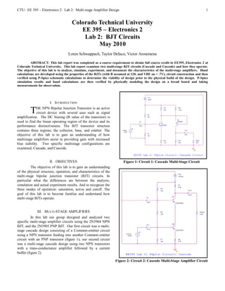
  • 1. CTU: EE 395 – Electronics 2: Lab 2: Multi-stage Amplifier Design 1 Colorado Technical University EE 395 – Electronics 2 Lab 2: BJT Circuits May 2010 Loren Schwappach, Taylor DeIaco, Victor Arosemena ABSTRACT: This lab report was completed as a course requirement to obtain full course credit in EE395, Electronics 2 at Colorado Technical University. This lab report examines two multi-stage BJT circuits (Cascade and Cascode) and how they operate. The objective of this lab is to analyze, simulate, experiment, and document the characteristics of the multi-stage amplifiers. Hand calculations are developed using the properties of the BJTs (with B assumed at 120, and VBE on = .7V), circuit construction and then verified using P-Spice schematic calculations to determine the viability of design prior to the physical build of the design. P-Spice simulation results and hand calculations are then verified by physically modeling the design on a bread board and taking measurements for observation. I. INTRODUCTION T HE NPN Bipolar Junction Transistor is an active circuit device with several uses such as signal amplification. The DC biasing (B value of the transistor) is used to find the linear operating region of the device and its performance distinctiveness. The BJT transistor structure contains three regions; the collector, base, and emitter. The objective of this lab is to gain an understanding of how multistage amplifiers assist in providing gain with increased bias stability. Two specific multistage configurations are examined, Cascade, and Cascode. II. OBJECTIVES Figure 1: Circuit 1: Cascade Multi-Stage Circuit The objective of this lab is to gain an understanding of the physical structure, operation, and characteristics of the multi-stage bipolar junction transistor (BJT) circuits. In particular what the differences are between the analysis, simulation and actual experiment results. And to recognize the three modes of operation: saturation, active and cutoff. The goal of this lab is to become familiar and understand how multi-stage BJTs operate. III. MULTI-STAGE AMPLIFIERS In this lab our group designed and analyzed two specific multi-stage amplifier circuits using the 2N3904 NPN BJT, and the 2N3905 PNP BJT. Our first circuit was a multi- stage cascade design consisting of a Common-emitter circuit using a NPN transistor feeding into another Common-emitter circuit with an PNP transistor (figure 1), our second circuit was a multi-stage cascode design using two NPN transistors with a trans-conductance amplifier followed by a current buffer (figure 2). Figure 2: Circuit 2: Cascode Multi-Stage Amplifier Circuit
  • 2. CTU: EE 395 – Electronics 2: Lab 2: Multi-stage Amplifier Design 2 IV. DESIGN APPROACHES/TRADE-OFFS The performance of this lab will depend on how well the circuits are developed. If the circuit is developed correctly the results showed should be similar to the hand calculation and PSpice simulation results. PSpice will be used to provide a rough estimate of what should be expected in the circuit measurements; however, the PSpice model transistor B tends to vary by the model, so the PSpice simulations could have a much larger error margin than the expected. The performance of the lab also depends on how well the equipment is calibrated and accurate the components tolerance is. This is not a very cost effective lab except for the development and time it took to construct the lab components. But to save money for a lab project, whether it’s the testing or developing phase of a new design, depending on what the schematic is, a circuit can be reduced, if done correctly. V. HAND CALCULATIONS The scanned hand calculations used for this lab can be found below. Figure 4: Circuit 2, Cascode Amplifier Hand Calculations. VI. CIRCUIT SCHEMATICS The final circuit schematics below were built in PSpice and allowed our team to analyze the circuit digitally before performing the physical build. However, since the B value of the transistor used is rarely the exact B of the transistor there is a margin of percentage error attributed. Figure 3: Circuit 1, Cascade Amplifier hand calculations. Figure 5: Circuit 1: Cascade Amplifier Voltages
  • 3. CTU: EE 395 – Electronics 2: Lab 2: Multi-stage Amplifier Design 3 Figure 6: Circuit 1: Cascade Amplifier Currents Figure 9: Circuit 2: Cascode Amplifier Currents Figure 7: Circuit 1: Cascade Amplifier Power Figure 10: Circuit 2: Cascode Amplifier Power In this lab we were also asked to find the frequency response and gain of the cascade and cascode multi-stage amplifier circuits. The PSpice results for both circuit designs follows.. Figure 8: Circuit 2: Cascode Amplifier Voltages
  • 4. CTU: EE 395 – Electronics 2: Lab 2: Multi-stage Amplifier Design 4 Figure 11: Circuit 1: Cascade Amplifier Bode Plot. Note lower (high pass) corner frequency is 2.4 Hz, higher (low pass) corner frequency is 1.25 MHz. Center frequency is 1.59 kHz which is what was used in this lab. Figure 13: Circuit 1: Cascade Amplifier Bode Plot. Note Stage 1 gain is 5.16, Stage 2 is 1.82, total gain is 9.4. Figure 12: Circuit 2: Cascode Amplifier Bode Plot. Note lower (high pass) corner frequency is 4 Hz, higher (low pass) corner frequency is 25 MHz. Center frequency is 12.6 kHz which is what was used in this lab. Figure 14: Circuit 2: Cascode Amplifier Bode Plot. Note gain is 5.42.
  • 5. CTU: EE 395 – Electronics 2: Lab 2: Multi-stage Amplifier Design 5 VII. COMPONENT LIST Hand The following is a list of components that were used in Calculated Pspice Actual constructing the BJT switch / inverter. Component values Results Results Results were selected by the professor. Vcc 10 V 10 V 10.02 V Vb1 2.17 V 2.063 V 2.086 V  A digital multimeter for measuring circuit voltages, resistor resistances, and capacitor Vb2 1.09 V 1.007 V 1.023 V capacitance. Ve2 390 mV 354.1 mV 363 mV  A power supply capable of delivering a constant Vc2 1.47 V 1.411 V 1.426 V Vcc = 10V. Vce2 1.08 V 1.057 V 1.063 V  Two 2N3904 NPN Transistor Vc1 5.47 V 5.877 V 5.898 V  One 2N3905 PNP Transistor  Applicable resisters for both multi-stage designs of Vce1 4V 4.466 V 4.472 V values approx 82k, 10k*2, 6.8k*3, 1.82k, 1.2k, Ib1 6 uA 4.669 uA 4.6 uA 72k, 575. Ic1 666 uA 621.9 uA 621.9 uA  Bread board with wires. Ie1 672 uA 626.5 uA 626.5 uA  NOTE: Resistors can normally provide around +/- 5%-25% difference between actual and designed Ib2 4 uA 4.8 uA 4.8 uA values while Capacitors generally provide around Ic2 672 uA 626.5 uA 626.5 uA 20%-50% difference between actual and designed Ie2 678 uA 631.3 uA 631.3 uA values. You can add resisters in series as (R1+R2) to closer approximate required resistance values Table 2: Circuit 2: Cascode Circuit: Comparison of Hand and you can add Capacitors in parallel as (C1+C2) Calculated, PSpice, and Measured Values. Notice all to closely approximate required capacitance. values are very close. This lab also asked for an analysis of the actual gain vs. VIII. EXPERIMENTAL DATA PSpice predicted. Results follow.. The following table illustrates the measurements taken at each stage of the lab. Pspice Actual Results Results Hand At Q1c 5.1647 4.88 Calculated Pspice Actual Cascade At Q2c 1.8195 1.85 Results Results Results Total Gain 9.397 9 Vcc 10 V 10 V 10.02 V At Q1c 5.41955 5 Vb1 1.087 V 1.062 V 1.058 V Cascode Total Gain 5.41955 5 Ve1 387 mV 425.4 mV 418 mV Vce1 7.437 V 7.2156 V 7.22 V IX. ANALYSIS/DATA COMPARISON Vc1 7.824 V 7.641 V 7.638 V Vce2 3.064 V 2.18 V 2.185 V The analysis/PSpice/Experimental data results were Ve2 8.524 V 8.342 V 8.35 V all accurate, but the results differed between the three. The reasons that the results were different is because the Vc2 5.46 V 6.162 V 6.165 V experimental results have equipment calibrations, component Ib1 3 uA 2.838 uA 2.6 uA tolerances, and actual measures values from the components. Ic1 320 uA 351.7 uA 347 uA The PSpice were less accurate than hand calculation because the PSpice B. All three results were not in total agreement Ie1 323 uA 354.5 uA 350 uA however, the results were close to each other. Ib2 7 uA -4.697 uA -6 uA Ic2 803 uA 906.2 uA 901 uA X. CONCLUSIONS Ie2 810 uA 910.9 uA 907 uA The discrepancies between the actual results, hand Table 1: Circuit 1: Cascade Circuit: Comparison of Hand calculated and simulated result is that they were all extremely Calculated, PSpice, and Measured Values. Notice all close (<20%) from the P-Spice results, however these results values are very close. could differ depending upon the error provided by the passive and active components, factors such as component tolerances, equipment calibrations and measurements fluctuations by the observer can contribute to results being slightly off from the
  • 6. CTU: EE 395 – Electronics 2: Lab 2: Multi-stage Amplifier Design 6 P-Spice calculations. It is always good to start with P-Spice to understand what is happening prior to build, and even more important to know the characteristics (B value) of the transistor. In conclusion, this lab was a great demonstration on the powerful features of multistage BJTs and their use in electronics. REFERENCES [1] D. A. Neamen, “Microelectronics: circuit analysis and design - 3rd ed.” McGraw-Hill, New York, NY, 2007. pp. 1-107.