SlideShare ist ein Scribd-Unternehmen logo
1 von 10
Module 11
Lecture – 03
Organization of Intel 8086 Microprocessor
Intel 8086 was the first 16-bit microprocessor introduced by Intel in 1978.
Register Organization of 8086
All the registers of 8086 are 16-bit registers. The general purpose registers can be used as
either 8-bit registers or 16-bit registers.
The register set of 8086 can be categorized into 4 different groups. The register
organization of 8086 is shown in the figure.
AX
BX
CX
DX
General data registers Segment Pointers and index
Registers registers
Register organization of 8086
General Data Registers:
The registers AX, BX,CX and DX are the general purpose 16-bit registers.
AX is used as 16-bit accumulator. The lower 8-bit is designated as AL and higher 8-bit is
designated as AH. AL can be used as an 8-bit accumulator for 8-bit operation.
All data register can be used as either 16 bit or 8 bit. BX is a 16 bit register, but BL
indicates the lower 8-bit of BX and BH indicates the higher 8-bit of BX.
The register CX is used default counter in case of string and loop instructions.
The register BX is used as offset storage for forming physical address in case of certain
addressing modes.
DX register is a general purpose register which may be used as an implicit operand or
destination in case of a few instructions.
Segment Registers:
AH AL
BH BL
CH CL
DH DL
SS
DS
ES
FLAGS/
PSW
BP
SI
DI
IP
The 8086 architecture uses the concept of segmented memory. 8086 able to address to
address a memory capacity of 1 megabyte and it is byte organized. This 1 megabyte
memory is divided into 16 logical segments. Each segment contains 64 kbytes of
memory.
There are four segment register in 8086
• Code segment register (CS)
• Data segment register (DS)
• Extra segment register (ES)
• Stack segment register (SS)
Code segment register (CS): is used fro addressing memory location in the code segment
of the memory, where the executable program is stored.
Data segment register (DS): points to the data segment of the memory where the data is
stored.
Extra Segment Register (ES) : also refers to a segment in the memory which is another
data segment in the memory.
Stack Segment Register (SS): is used fro addressing stack segment of the memory. The
stack segment is that segment of memory which is used to store stack data.
While addressing any location in the memory bank, the physical address is calculated
from two parts:
- The first is segment address, the segment registers contain 16-bit segment base
addresses, related to different segment.
- The second part is the offset value in that segment.
The advantage of this scheme is that in place of maintaining a 20-bit register for a
physical address, the processor just maintains two 16-bit registers which is within the
memory capacity of the machine.
Pointers and Index Registers.
The pointers contain offset within the particular segments.
- The pointer register IP contains offset within the code segment.
- The pointer register BP contains offset within the data segment.
- He pointer register SP contains offset within the stack segment.
The index registers are used as general purpose registers as well as for offset storage in
case of indexed, base indexed and relative base indexed addressing modes.
The register SI is used to store the offset of source data in data segment.
The register DI is used to store the offset of destination in data or extra segment.
The index registers are particularly useful for string manipulation.
Flag Register
The 8086 flag register contents indicate the results of computation in the ALU. It also
contains some flag bits to control the CPU operations.
8086 Architecture:
The 8086 architecture supports
- a 16-bit ALU.
- a set of 16 bit registers
- provides segmented memory addressing scheme
- a rich instruction set.
- Powerful interrupt structure
- Fetched instruction queue for overlapped fetching and execution step.
The internal block diagram units inside the 8086 microprocessor is shown in the figure.
FIG
The architecture of 8086 can be divided into two parts
(a) Bus Interface unit (BIU)
(b) Execution unit (EU)
The bus interface unit is responsible for physical address calculations and a predecoding
instruction byte queue ( 6 bytes long).
The bus interface unit makes the system bus signal available for external devices.
The 8086 addresses a segmented memory. The complete physical address which is 20-
bits long is generated using segment and offset registers, each 16-bits long.
Generating a physical address:
- The content of segment register (segment address) is shifted left bit-wise four
times.
- The content of an offset register (offset address) is added to the result of the
previous shift operation.
These two operations together produce a 20-bit physical address.
For example, consider the segment address is 2010H and the offset address is 3535H.
The physical address is calculated as:
Segment Address 2010H 0 0 1 0 0 0 0 0 0 0 0 1 0 0 0 0
Shifted left by
4 bit positions 0 0 1 0 0 0 0 0 0 0 0 1 0 0 0 0 0 0 0 0
+
offset address 0 0 1 1 0 1 0 1 0 0 1 1 0 1 0 1
---------------------------------------------------------------
physical address 0 0 1 0 0 0 1 1 0 1 1 0 0 0 1 1 0 1 0 1
2 3 6 3 5
The segment address by the segment value 2010H can have offset value from 0000H to
FFFFH within it, ie. Maximum 64K locations may be accommodated in the segment.
The physical address range for this segment is from 20100H to 300FFH.
The segment register indicates the base address of a particular segment and CS, DS, SS
and ES are used to keep the segment address.
The offset indicates the distance of the required memory location in the segment from the
base address, and the offset may be the content of register IP, BP, SI, DI and SP.
Once the opcode is fetched and decoded, the external bus becomes free while the
Execution Unit is executing the instruction.
While the fetched instruction is executed internally, the external bus is used to fetch the
machine code of the next instruction and arrange it in a queue called as predecoded
instruction byte queue.
This is a 6 byte long queue, works in first-in first-out policy.
While the opcode is fetched by the bus interface unit (BIU), the execution unit (EU)
executes the previously decoded instruction concurrently.
The execution unit contains.
- the register set of 8086 except segment registers and IF.
- a 16-bit ALU to perform arithmetic & logic operation
- 16-bit flag register reflects the results of execution by the ALU.
- the decoding units decodes the op-code bytes issued from the instruction byte
queue.
- the timing and control unit generates the necessary control signals to execute the
instruction op-code received from the queue.
The execution unit may pass the results to the bus interface unit for storing them in
memory.
Memory Segmentation:
The size of address bus of 8086 is 20 and is able to address 1 Mbytes ( 20
2 ) of physical
memory.
The compete 1 Mbytes memory can be divided into 16 segments, each of 16 Kbytes size.
The addresses of the segment may be assigned as 0000H to F000H respectively.
The offset values are from 0000H to FFFFFH.
If the segmentation is done as per above mentioned way, the segments are called non-
overlapping segments.
In some cases segment may overlap also. Suppose a segment starts at a particular address
and its maximum size can go up to 64 Kbytes. But if another segment starts before this 64
Kbytes location of the first segment, the two segments are said to be overlapping
segment.
The area of memory from the start of the second segment to the possible end of the first
segment is called as overlapped segment.
Non-overlapping segments and overlapping segments are shown in the figure.
Fig
Non-Overlapping Segments
The main advantages of the segmented memory scheme are as follows:
a) Allows the memory capacity to be 1 Mbyte although the actual addresses to be
handled are of 16-bit size
b) Allows the placing of code data and stack portions of the same program in
different parts (segments) of memory, for data and code protection.
c) Permits a program and/ or its data to be put into different areas of memory each
time program is executed, ie, provision for relocation may be done.
Flag Register
A 16 flag register is used in 8086. It is divided into two parts .
(a) Condition code or status flags
(b) Machine control flags
The condition code flag register is the lower byte of the 16-bit flag register. The condition
code flag register is identical to 8085 flag register, with an additional overflow flag.
The control flag register is the higher byte of the flag register. It contains three flags
namely direction flag(D), interrupt flag (I) and trap flag (T).
The complete bit configuration of 8086 is shown in the figure.
15 14 13 12 11 10 9 8 7 6 5 4 3 2 1 0
S- Sign Flag : This flag is set, when the result of any computation is negative.
Z- Zero Flag: This flag is set, if the result of the computation or comparison performed
by the previous instruction is zero.
P- Parity Flag: This flag is set to 1, if the lower byte of the result contains even number
of 1’s.
C- Carry Flag: This flag is set, when there is a carry out of MSB in case of addition or a
borrow in case of subtraction.
T- Tarp Flag: If this flag is set, the processor enters the single step execution mode.
I- Interrupt Flag: If this flag is set, the maskable interrupt are recognized by the CPU,
otherwise they are ignored.
D- Direction Flag: This is used by string manipulation instructions. If this flag bit is ‘0’,
the string is processed beginning from the lowest address to the highest address, i.e.,
auto incrementing mode. Otherwise, the string is processed from the highest address
towards the lowest address, i.e., auto incrementing mode.
AC-Auxilary Carry Flag: This is set, if there is a carry from the lowest nibble, i.e, bit
three during addition, or borrow for the lowest nibble, i.e, bit three, during
subtraction.
O- Over flow Flag: This flag is set, if an overflow occurs, i.e, if the result of a signed
operation is large enough to accommodate in a destination register. The result is of
more than 7-bits in size in case of 8-bit signed operation and more than 15-bits in size
in case of 16-bit sign operations, then the overflow will be set.
Signals of 8086
The 8086 is a 16-bit microprocessor. This microprocessor operate in single processor or
multiprocessor configurations to achieve high performance. The pin configuration of
8086 is shown in the figure. Some of the pins serve a particular function in minimum
mode (single processor mode) and others function in maximum mode (multiprocessor
mode).
FIG
Description of signals of 8086
X X X X 0 D I T S Z X AC X P X CY
7 0AD AD− The address/ data bus lines are the multiplexed address data bus and contain
the right most eight bit of memory address or data. The address and data bits
are separated by using ALE signal.
15 8AD AD− The address/data bus lines compose the upper multiplexed address/data bus.
This lines contain address bit 15 8A A− or data bus 15 8D D− . The address and
data bits are separated by using ALE signal.
19 6 18 3/ /A S A S− The address/status bus bits are multiplexed to provide address signals
19 16A A− and also status bits 6 3S S− . The address bits are separated
from the status bits using the ALE signals. The status bit 6S is always
a logic 0, bit 5S indicates the condition of the interrupt flag bit. The
4S and 3S combinedly indicate which segment register is presently
being used for memory access.
7/BHE S The bus high enable (BHE) signal is used to indicate the transfer of data over
the higher order ( )15 8D D− data bus. It goes low for the data transfer over
15 8D D− and is used to derive chip select of odd address memory bank or
peripherals.
4S 3S Funtion
0 0 Extra segment
0 1 Stack segment
1 0 Code or no segment
1 1 Data Segment
BHE 0A Indication
0 0 Whole word
0 1 Upper byte from or to odd address
1 0 Lower byte from or to even address
1 1 None
RD : Read : whenever the read signal is at logic 0, the data bus receives the data from
the memory or 0π devices connected to the system
READY :This is the acknowledgement from the slow devices or memory that they have
completed the data transfer operation. This signal is active high.
INTR: Interrupt Request: Interrupt request is used to request a hardware interrupt of INTR
is held high when interrupt enable flag is set, the 8086 enters an interrupt
acknowledgement cycle after the current instruction has completed its execution.
TEST : This input is tested by “WAIT” instruction. If the TEST input goes low;
execution will continue. Else the processor remains in an idle state.
NMI- Non-maskable Interrupt: The non-maskable interrupt input is similar to INTR
except that the NMI interrupt does not check for interrupt enable flag is at logic 1,
i.e, NMI is not maskable internally by software. If NMI is activated, the interrupt
input uses interrupt vector 2.
RESET: The reset input causes the microprocessor to reset itself. When 8086 reset, it
restarts the execution from memory location FFFF0H. The reset signal is active
high and must be active for at least four clock cycles.
CLK : Clock input: The clock input signal provides the basic timing input signal for
processor and bus control operation. It is asymmetric square wave with 33% duty
cycle.
ccV 5V+ power supply for the operation of the internal circuit
COND Ground for the internal circuit
/MN MX : The minimum/maximum mode signal to select the mode of operation either in
minimum or maximum mode configuration. Logic 1 indicates minimum mode.
Minimum mode Signals: The following signals are for minimum mode operation of
8086.
/M IO -Memory/IO /M IO signal selects either memory operation or oπ operation.
This line indicates that the microprocessor address bus contains either a memory
address or an oπ port address. Signal high at this pin indicates a memory
operation. This line is logically equivalent to 2S in maximum mode.
INTA - Interrupt acknowledge: The interrupt acknowledge signal is a response to the
INTR input signal. The INTA signal is normally used to gate the interrupt vector
number onto the data bus in response to an interrupt request.
ALE- Address Latch Enable: This output signal indicates the availability of valid address
on the address/data bus, and is connected to latch enable input of latches.
/DT R : Data transmit/Receive: This output signal is used to decide the direction of date
flow through the bi-directional buffer. / 1DT R = indicates transmitting and
/ 0DT R = indicates receiving the data.
DEN Data Enable: Data bus enable signal indicates the availability of valid data over
the address/data lines.
HOLD: The hold input request a direct memory access(DMA). If the hold signal is at
logic 1, the micro process stops its normal execution and places its address, data
and control bus at the high impedance state.
HLDA: Hold acknowledgement indicates that 8086 has entered into the hold state.
Maximum mode signal: The following signals are for maximum mode operation of 8086.
2 1 0, ,S S S - Status lines: These are the status lines that reflect the type of operation being
carried out by the processor.
These status lines are encoded as follows
2S 1S 0S Function
0 0 0 Interrupt Acknowledge
0 0 1 Read oπ port
0 1 0 Write oπ port
0 1 1 Halt
1 0 0 Code Access
1 0 1 Read memory
1 1 0 Write memory
1 1 1 passive
LOCK : The lock output is used to lock peripherals off the system, ie, the other system
bus masters will be prevented from gaining the system bus.
1QS and 0QS - Queue status: The queue status bits shows the status of the internal
instruction queue. The encoding of these signals is as follows
1QS 0QS Function
0 0 No operation, queue is idle
0 1 First byte of opcode
1 0 Queue is empty
1 1 Subsequent byte of opcode
/ 1RQ GT and / 0RQ GT - request/Grant: The request/grant pins are used by other local
bus masters to force the processor to release the local bus at the end of the
processors current bus cycle. These lines are bi-directional and are used to both
request and grant a DMA operation. / 0RQ GT is having higher priority than
/ 1RQ GT
Physical Memory Organization
In an 8086 based system, the 1Mbyte memory is physically organized as odd bank and
even bank, each of 512kbytes, addressed in parallel by the processor.
Byte data with even address is transferred on 7 0D D− and byte data with odd address is
transferred on 15 8D D− .
The processor provides two enable signals, BHE and 0A for selecting of either even or
odd or both the banks.
FIG
BHE 0A Function
0 0 Whole word
0 1 Upper byte/ odd address
1 0 Lower byte/even address
1 1 none
If the address bus contains HFFFFO
If 0BHE = , then it reads the 16 bits data from memory location HFFFFO and 1HFFFF .
If 1BHE = , it reads the 8 bits data from memory location HFFFFO
15 0 15 0/D D A A− − are the
common signal line in 8086 as
15 0AD AD−

Weitere ähnliche Inhalte

Was ist angesagt?

Register introduction
Register introductionRegister introduction
Register introductionmaamir farooq
 
PAI Unit 3 Multitasking in 80386
PAI Unit 3 Multitasking in 80386PAI Unit 3 Multitasking in 80386
PAI Unit 3 Multitasking in 80386KanchanPatil34
 
Flags registor of 8086 processor
Flags registor of 8086 processorFlags registor of 8086 processor
Flags registor of 8086 processorFazle Akash
 
Time delay programs and assembler directives 8086
Time delay programs and assembler directives 8086Time delay programs and assembler directives 8086
Time delay programs and assembler directives 8086Dheeraj Suri
 
8086 architecture and pin description
8086 architecture and pin description 8086 architecture and pin description
8086 architecture and pin description Aswini Dharmaraj
 
Introduction to 80386
Introduction to 80386Introduction to 80386
Introduction to 80386Abinaya B
 
Logic, shift and rotate instruction
Logic, shift and rotate instructionLogic, shift and rotate instruction
Logic, shift and rotate instructionkashif Shafqat
 
Advanced Microprocessors By Er. Swapnil Kaware
Advanced Microprocessors By Er. Swapnil KawareAdvanced Microprocessors By Er. Swapnil Kaware
Advanced Microprocessors By Er. Swapnil KawareProf. Swapnil V. Kaware
 
Register of 80386
Register of 80386Register of 80386
Register of 80386aviban
 
Addressing modes of 80386
Addressing modes of 80386Addressing modes of 80386
Addressing modes of 80386PDFSHARE
 

Was ist angesagt? (20)

80386
8038680386
80386
 
Register introduction
Register introductionRegister introduction
Register introduction
 
PAI Unit 3 Multitasking in 80386
PAI Unit 3 Multitasking in 80386PAI Unit 3 Multitasking in 80386
PAI Unit 3 Multitasking in 80386
 
8086
8086 8086
8086
 
8086 architecture
8086 architecture8086 architecture
8086 architecture
 
Chapter 1 archietecture of 8086
Chapter 1 archietecture of 8086Chapter 1 archietecture of 8086
Chapter 1 archietecture of 8086
 
Flags registor of 8086 processor
Flags registor of 8086 processorFlags registor of 8086 processor
Flags registor of 8086 processor
 
Time delay programs and assembler directives 8086
Time delay programs and assembler directives 8086Time delay programs and assembler directives 8086
Time delay programs and assembler directives 8086
 
8086 architecture and pin description
8086 architecture and pin description 8086 architecture and pin description
8086 architecture and pin description
 
8051 presentation
8051 presentation8051 presentation
8051 presentation
 
Introduction to 80386
Introduction to 80386Introduction to 80386
Introduction to 80386
 
Logic, shift and rotate instruction
Logic, shift and rotate instructionLogic, shift and rotate instruction
Logic, shift and rotate instruction
 
Intel+80286
Intel+80286Intel+80286
Intel+80286
 
Advanced Microprocessors By Er. Swapnil Kaware
Advanced Microprocessors By Er. Swapnil KawareAdvanced Microprocessors By Er. Swapnil Kaware
Advanced Microprocessors By Er. Swapnil Kaware
 
80386 & 80486
80386 & 8048680386 & 80486
80386 & 80486
 
80386-1.pptx
80386-1.pptx80386-1.pptx
80386-1.pptx
 
8086 architecture By Er. Swapnil Kaware
8086 architecture By Er. Swapnil Kaware8086 architecture By Er. Swapnil Kaware
8086 architecture By Er. Swapnil Kaware
 
Register of 80386
Register of 80386Register of 80386
Register of 80386
 
Addressing modes of 80386
Addressing modes of 80386Addressing modes of 80386
Addressing modes of 80386
 
Registers
RegistersRegisters
Registers
 

Andere mochten auch

Ch2 microcontroller architecture
Ch2 microcontroller architectureCh2 microcontroller architecture
Ch2 microcontroller architectureAhmad Sidik
 
Three Central Processing Unit
Three   Central Processing UnitThree   Central Processing Unit
Three Central Processing UnitMISY
 
Central processing unit
Central processing unitCentral processing unit
Central processing unitKumar
 
Computer Organization Lecture Notes
Computer Organization Lecture NotesComputer Organization Lecture Notes
Computer Organization Lecture NotesFellowBuddy.com
 
Memory Management in Windows 7
Memory Management in Windows 7Memory Management in Windows 7
Memory Management in Windows 7Naveed Qadri
 
Central processing unit
Central processing unitCentral processing unit
Central processing unitKamal Acharya
 
Architecture of 80286 microprocessor
Architecture of 80286 microprocessorArchitecture of 80286 microprocessor
Architecture of 80286 microprocessorSyed Ahmed Zaki
 
8086 class notes-Y.N.M
8086 class notes-Y.N.M8086 class notes-Y.N.M
8086 class notes-Y.N.MDr.YNM
 
Assembly language programming(unit 4)
Assembly language programming(unit 4)Assembly language programming(unit 4)
Assembly language programming(unit 4)Ashim Saha
 

Andere mochten auch (10)

Ch2 microcontroller architecture
Ch2 microcontroller architectureCh2 microcontroller architecture
Ch2 microcontroller architecture
 
Three Central Processing Unit
Three   Central Processing UnitThree   Central Processing Unit
Three Central Processing Unit
 
Central processing unit
Central processing unitCentral processing unit
Central processing unit
 
Computer Organization Lecture Notes
Computer Organization Lecture NotesComputer Organization Lecture Notes
Computer Organization Lecture Notes
 
Memory Management in Windows 7
Memory Management in Windows 7Memory Management in Windows 7
Memory Management in Windows 7
 
Central processing unit
Central processing unitCentral processing unit
Central processing unit
 
Architecture of 80286 microprocessor
Architecture of 80286 microprocessorArchitecture of 80286 microprocessor
Architecture of 80286 microprocessor
 
Cpu ppt cse
Cpu ppt cseCpu ppt cse
Cpu ppt cse
 
8086 class notes-Y.N.M
8086 class notes-Y.N.M8086 class notes-Y.N.M
8086 class notes-Y.N.M
 
Assembly language programming(unit 4)
Assembly language programming(unit 4)Assembly language programming(unit 4)
Assembly language programming(unit 4)
 

Ähnlich wie 3 organization of intel 8086

microprocessor_part_3_compressed_1588259301.pdf
microprocessor_part_3_compressed_1588259301.pdfmicroprocessor_part_3_compressed_1588259301.pdf
microprocessor_part_3_compressed_1588259301.pdfssuserd21262
 
Intel Microprocessors 8086 Documentation
Intel Microprocessors 8086 DocumentationIntel Microprocessors 8086 Documentation
Intel Microprocessors 8086 DocumentationAdeel Rasheed
 
26677766 8086-microprocessor-architecture
26677766 8086-microprocessor-architecture26677766 8086-microprocessor-architecture
26677766 8086-microprocessor-architectureSaurabh Jain
 
8086 microprocessor-architecture-120207111857-phpapp01
8086 microprocessor-architecture-120207111857-phpapp018086 microprocessor-architecture-120207111857-phpapp01
8086 microprocessor-architecture-120207111857-phpapp01destaw belay
 
8086 microprocessor-architecture-120207111857-phpapp01
8086 microprocessor-architecture-120207111857-phpapp018086 microprocessor-architecture-120207111857-phpapp01
8086 microprocessor-architecture-120207111857-phpapp01Siva Raman
 
Presentation on 8086 microprocessor
Presentation on 8086 microprocessorPresentation on 8086 microprocessor
Presentation on 8086 microprocessorDiponkor Bala
 
Intel 8086 microprocessor
Intel 8086 microprocessorIntel 8086 microprocessor
Intel 8086 microprocessorRavi Yasas
 
physical_address segmentation.pdf
physical_address segmentation.pdfphysical_address segmentation.pdf
physical_address segmentation.pdfSwapnil511014
 
INTEL 8086 MICROPROCESSOR
INTEL 8086 MICROPROCESSORINTEL 8086 MICROPROCESSOR
INTEL 8086 MICROPROCESSORSagar Kuntumal
 
introduction to Architecture of 8086 and it's application
introduction to Architecture of 8086 and it's applicationintroduction to Architecture of 8086 and it's application
introduction to Architecture of 8086 and it's applicationDrVikasMahor
 

Ähnlich wie 3 organization of intel 8086 (20)

microprocessor_part_3_compressed_1588259301.pdf
microprocessor_part_3_compressed_1588259301.pdfmicroprocessor_part_3_compressed_1588259301.pdf
microprocessor_part_3_compressed_1588259301.pdf
 
Advanced micro -processor
Advanced micro -processorAdvanced micro -processor
Advanced micro -processor
 
Intel Microprocessors 8086 Documentation
Intel Microprocessors 8086 DocumentationIntel Microprocessors 8086 Documentation
Intel Microprocessors 8086 Documentation
 
8086 archi notes final
8086 archi notes final8086 archi notes final
8086 archi notes final
 
8086 archi notes final
8086 archi notes final8086 archi notes final
8086 archi notes final
 
Chapter 2
Chapter 2Chapter 2
Chapter 2
 
Arch 8086
Arch 8086Arch 8086
Arch 8086
 
26677766 8086-microprocessor-architecture
26677766 8086-microprocessor-architecture26677766 8086-microprocessor-architecture
26677766 8086-microprocessor-architecture
 
8086 microprocessor-architecture-120207111857-phpapp01
8086 microprocessor-architecture-120207111857-phpapp018086 microprocessor-architecture-120207111857-phpapp01
8086 microprocessor-architecture-120207111857-phpapp01
 
8086 microprocessor-architecture-120207111857-phpapp01
8086 microprocessor-architecture-120207111857-phpapp018086 microprocessor-architecture-120207111857-phpapp01
8086 microprocessor-architecture-120207111857-phpapp01
 
lec 2.pptx
lec 2.pptxlec 2.pptx
lec 2.pptx
 
Presentation on 8086 microprocessor
Presentation on 8086 microprocessorPresentation on 8086 microprocessor
Presentation on 8086 microprocessor
 
Intel 8086 microprocessor
Intel 8086 microprocessorIntel 8086 microprocessor
Intel 8086 microprocessor
 
physical_address segmentation.pdf
physical_address segmentation.pdfphysical_address segmentation.pdf
physical_address segmentation.pdf
 
8086
80868086
8086
 
8086
80868086
8086
 
INTEL 8086 MICROPROCESSOR
INTEL 8086 MICROPROCESSORINTEL 8086 MICROPROCESSOR
INTEL 8086 MICROPROCESSOR
 
Mpi chapter 2
Mpi chapter 2Mpi chapter 2
Mpi chapter 2
 
introduction to Architecture of 8086 and it's application
introduction to Architecture of 8086 and it's applicationintroduction to Architecture of 8086 and it's application
introduction to Architecture of 8086 and it's application
 
8086 PPt-2021.pptx
8086 PPt-2021.pptx8086 PPt-2021.pptx
8086 PPt-2021.pptx
 

Mehr von ELIMENG

Get started with dropbox
Get started with dropboxGet started with dropbox
Get started with dropboxELIMENG
 
07 chap3
07 chap307 chap3
07 chap3ELIMENG
 
6 wordiness(1)
6 wordiness(1)6 wordiness(1)
6 wordiness(1)ELIMENG
 
6 wordiness
6 wordiness6 wordiness
6 wordinessELIMENG
 
6 friction fe
6 friction fe6 friction fe
6 friction feELIMENG
 
06 9 1_balboa
06 9 1_balboa06 9 1_balboa
06 9 1_balboaELIMENG
 
05 chap 4 research methodology and design(1)
05 chap 4 research methodology and design(1)05 chap 4 research methodology and design(1)
05 chap 4 research methodology and design(1)ELIMENG
 
05 chap 4 research methodology and design
05 chap 4 research methodology and design05 chap 4 research methodology and design
05 chap 4 research methodology and designELIMENG
 
4.2.cappelli 06(3)
4.2.cappelli 06(3)4.2.cappelli 06(3)
4.2.cappelli 06(3)ELIMENG
 
4.2.cappelli 06(2)
4.2.cappelli 06(2)4.2.cappelli 06(2)
4.2.cappelli 06(2)ELIMENG
 
4.2.cappelli 06(1)
4.2.cappelli 06(1)4.2.cappelli 06(1)
4.2.cappelli 06(1)ELIMENG
 

Mehr von ELIMENG (20)

Get started with dropbox
Get started with dropboxGet started with dropbox
Get started with dropbox
 
8
88
8
 
07 chap3
07 chap307 chap3
07 chap3
 
7 4
7 47 4
7 4
 
6 wordiness(1)
6 wordiness(1)6 wordiness(1)
6 wordiness(1)
 
6 wordiness
6 wordiness6 wordiness
6 wordiness
 
6 friction fe
6 friction fe6 friction fe
6 friction fe
 
06 3
06 306 3
06 3
 
06 9 1_balboa
06 9 1_balboa06 9 1_balboa
06 9 1_balboa
 
05 chap 4 research methodology and design(1)
05 chap 4 research methodology and design(1)05 chap 4 research methodology and design(1)
05 chap 4 research methodology and design(1)
 
05 chap 4 research methodology and design
05 chap 4 research methodology and design05 chap 4 research methodology and design
05 chap 4 research methodology and design
 
5 6
5 65 6
5 6
 
5
55
5
 
04 99
04 9904 99
04 99
 
4 2(1)
4 2(1)4 2(1)
4 2(1)
 
4 2
4 24 2
4 2
 
04
0404
04
 
4.2.cappelli 06(3)
4.2.cappelli 06(3)4.2.cappelli 06(3)
4.2.cappelli 06(3)
 
4.2.cappelli 06(2)
4.2.cappelli 06(2)4.2.cappelli 06(2)
4.2.cappelli 06(2)
 
4.2.cappelli 06(1)
4.2.cappelli 06(1)4.2.cappelli 06(1)
4.2.cappelli 06(1)
 

3 organization of intel 8086

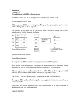
  • 1. Module 11 Lecture – 03 Organization of Intel 8086 Microprocessor Intel 8086 was the first 16-bit microprocessor introduced by Intel in 1978. Register Organization of 8086 All the registers of 8086 are 16-bit registers. The general purpose registers can be used as either 8-bit registers or 16-bit registers. The register set of 8086 can be categorized into 4 different groups. The register organization of 8086 is shown in the figure. AX BX CX DX General data registers Segment Pointers and index Registers registers Register organization of 8086 General Data Registers: The registers AX, BX,CX and DX are the general purpose 16-bit registers. AX is used as 16-bit accumulator. The lower 8-bit is designated as AL and higher 8-bit is designated as AH. AL can be used as an 8-bit accumulator for 8-bit operation. All data register can be used as either 16 bit or 8 bit. BX is a 16 bit register, but BL indicates the lower 8-bit of BX and BH indicates the higher 8-bit of BX. The register CX is used default counter in case of string and loop instructions. The register BX is used as offset storage for forming physical address in case of certain addressing modes. DX register is a general purpose register which may be used as an implicit operand or destination in case of a few instructions. Segment Registers: AH AL BH BL CH CL DH DL SS DS ES FLAGS/ PSW BP SI DI IP
  • 2. The 8086 architecture uses the concept of segmented memory. 8086 able to address to address a memory capacity of 1 megabyte and it is byte organized. This 1 megabyte memory is divided into 16 logical segments. Each segment contains 64 kbytes of memory. There are four segment register in 8086 • Code segment register (CS) • Data segment register (DS) • Extra segment register (ES) • Stack segment register (SS) Code segment register (CS): is used fro addressing memory location in the code segment of the memory, where the executable program is stored. Data segment register (DS): points to the data segment of the memory where the data is stored. Extra Segment Register (ES) : also refers to a segment in the memory which is another data segment in the memory. Stack Segment Register (SS): is used fro addressing stack segment of the memory. The stack segment is that segment of memory which is used to store stack data. While addressing any location in the memory bank, the physical address is calculated from two parts: - The first is segment address, the segment registers contain 16-bit segment base addresses, related to different segment. - The second part is the offset value in that segment. The advantage of this scheme is that in place of maintaining a 20-bit register for a physical address, the processor just maintains two 16-bit registers which is within the memory capacity of the machine. Pointers and Index Registers. The pointers contain offset within the particular segments. - The pointer register IP contains offset within the code segment. - The pointer register BP contains offset within the data segment. - He pointer register SP contains offset within the stack segment. The index registers are used as general purpose registers as well as for offset storage in case of indexed, base indexed and relative base indexed addressing modes. The register SI is used to store the offset of source data in data segment.
  • 3. The register DI is used to store the offset of destination in data or extra segment. The index registers are particularly useful for string manipulation. Flag Register The 8086 flag register contents indicate the results of computation in the ALU. It also contains some flag bits to control the CPU operations. 8086 Architecture: The 8086 architecture supports - a 16-bit ALU. - a set of 16 bit registers - provides segmented memory addressing scheme - a rich instruction set. - Powerful interrupt structure - Fetched instruction queue for overlapped fetching and execution step. The internal block diagram units inside the 8086 microprocessor is shown in the figure. FIG The architecture of 8086 can be divided into two parts (a) Bus Interface unit (BIU) (b) Execution unit (EU) The bus interface unit is responsible for physical address calculations and a predecoding instruction byte queue ( 6 bytes long). The bus interface unit makes the system bus signal available for external devices. The 8086 addresses a segmented memory. The complete physical address which is 20- bits long is generated using segment and offset registers, each 16-bits long. Generating a physical address: - The content of segment register (segment address) is shifted left bit-wise four times. - The content of an offset register (offset address) is added to the result of the previous shift operation. These two operations together produce a 20-bit physical address. For example, consider the segment address is 2010H and the offset address is 3535H. The physical address is calculated as:
  • 4. Segment Address 2010H 0 0 1 0 0 0 0 0 0 0 0 1 0 0 0 0 Shifted left by 4 bit positions 0 0 1 0 0 0 0 0 0 0 0 1 0 0 0 0 0 0 0 0 + offset address 0 0 1 1 0 1 0 1 0 0 1 1 0 1 0 1 --------------------------------------------------------------- physical address 0 0 1 0 0 0 1 1 0 1 1 0 0 0 1 1 0 1 0 1 2 3 6 3 5 The segment address by the segment value 2010H can have offset value from 0000H to FFFFH within it, ie. Maximum 64K locations may be accommodated in the segment. The physical address range for this segment is from 20100H to 300FFH. The segment register indicates the base address of a particular segment and CS, DS, SS and ES are used to keep the segment address. The offset indicates the distance of the required memory location in the segment from the base address, and the offset may be the content of register IP, BP, SI, DI and SP. Once the opcode is fetched and decoded, the external bus becomes free while the Execution Unit is executing the instruction. While the fetched instruction is executed internally, the external bus is used to fetch the machine code of the next instruction and arrange it in a queue called as predecoded instruction byte queue. This is a 6 byte long queue, works in first-in first-out policy. While the opcode is fetched by the bus interface unit (BIU), the execution unit (EU) executes the previously decoded instruction concurrently. The execution unit contains. - the register set of 8086 except segment registers and IF. - a 16-bit ALU to perform arithmetic & logic operation - 16-bit flag register reflects the results of execution by the ALU. - the decoding units decodes the op-code bytes issued from the instruction byte queue. - the timing and control unit generates the necessary control signals to execute the instruction op-code received from the queue. The execution unit may pass the results to the bus interface unit for storing them in memory. Memory Segmentation:
  • 5. The size of address bus of 8086 is 20 and is able to address 1 Mbytes ( 20 2 ) of physical memory. The compete 1 Mbytes memory can be divided into 16 segments, each of 16 Kbytes size. The addresses of the segment may be assigned as 0000H to F000H respectively. The offset values are from 0000H to FFFFFH. If the segmentation is done as per above mentioned way, the segments are called non- overlapping segments. In some cases segment may overlap also. Suppose a segment starts at a particular address and its maximum size can go up to 64 Kbytes. But if another segment starts before this 64 Kbytes location of the first segment, the two segments are said to be overlapping segment. The area of memory from the start of the second segment to the possible end of the first segment is called as overlapped segment. Non-overlapping segments and overlapping segments are shown in the figure. Fig Non-Overlapping Segments The main advantages of the segmented memory scheme are as follows: a) Allows the memory capacity to be 1 Mbyte although the actual addresses to be handled are of 16-bit size b) Allows the placing of code data and stack portions of the same program in different parts (segments) of memory, for data and code protection. c) Permits a program and/ or its data to be put into different areas of memory each time program is executed, ie, provision for relocation may be done. Flag Register A 16 flag register is used in 8086. It is divided into two parts . (a) Condition code or status flags (b) Machine control flags The condition code flag register is the lower byte of the 16-bit flag register. The condition code flag register is identical to 8085 flag register, with an additional overflow flag. The control flag register is the higher byte of the flag register. It contains three flags namely direction flag(D), interrupt flag (I) and trap flag (T). The complete bit configuration of 8086 is shown in the figure.
  • 6. 15 14 13 12 11 10 9 8 7 6 5 4 3 2 1 0 S- Sign Flag : This flag is set, when the result of any computation is negative. Z- Zero Flag: This flag is set, if the result of the computation or comparison performed by the previous instruction is zero. P- Parity Flag: This flag is set to 1, if the lower byte of the result contains even number of 1’s. C- Carry Flag: This flag is set, when there is a carry out of MSB in case of addition or a borrow in case of subtraction. T- Tarp Flag: If this flag is set, the processor enters the single step execution mode. I- Interrupt Flag: If this flag is set, the maskable interrupt are recognized by the CPU, otherwise they are ignored. D- Direction Flag: This is used by string manipulation instructions. If this flag bit is ‘0’, the string is processed beginning from the lowest address to the highest address, i.e., auto incrementing mode. Otherwise, the string is processed from the highest address towards the lowest address, i.e., auto incrementing mode. AC-Auxilary Carry Flag: This is set, if there is a carry from the lowest nibble, i.e, bit three during addition, or borrow for the lowest nibble, i.e, bit three, during subtraction. O- Over flow Flag: This flag is set, if an overflow occurs, i.e, if the result of a signed operation is large enough to accommodate in a destination register. The result is of more than 7-bits in size in case of 8-bit signed operation and more than 15-bits in size in case of 16-bit sign operations, then the overflow will be set. Signals of 8086 The 8086 is a 16-bit microprocessor. This microprocessor operate in single processor or multiprocessor configurations to achieve high performance. The pin configuration of 8086 is shown in the figure. Some of the pins serve a particular function in minimum mode (single processor mode) and others function in maximum mode (multiprocessor mode). FIG Description of signals of 8086 X X X X 0 D I T S Z X AC X P X CY
  • 7. 7 0AD AD− The address/ data bus lines are the multiplexed address data bus and contain the right most eight bit of memory address or data. The address and data bits are separated by using ALE signal. 15 8AD AD− The address/data bus lines compose the upper multiplexed address/data bus. This lines contain address bit 15 8A A− or data bus 15 8D D− . The address and data bits are separated by using ALE signal. 19 6 18 3/ /A S A S− The address/status bus bits are multiplexed to provide address signals 19 16A A− and also status bits 6 3S S− . The address bits are separated from the status bits using the ALE signals. The status bit 6S is always a logic 0, bit 5S indicates the condition of the interrupt flag bit. The 4S and 3S combinedly indicate which segment register is presently being used for memory access. 7/BHE S The bus high enable (BHE) signal is used to indicate the transfer of data over the higher order ( )15 8D D− data bus. It goes low for the data transfer over 15 8D D− and is used to derive chip select of odd address memory bank or peripherals. 4S 3S Funtion 0 0 Extra segment 0 1 Stack segment 1 0 Code or no segment 1 1 Data Segment BHE 0A Indication 0 0 Whole word 0 1 Upper byte from or to odd address 1 0 Lower byte from or to even address 1 1 None
  • 8. RD : Read : whenever the read signal is at logic 0, the data bus receives the data from the memory or 0π devices connected to the system READY :This is the acknowledgement from the slow devices or memory that they have completed the data transfer operation. This signal is active high. INTR: Interrupt Request: Interrupt request is used to request a hardware interrupt of INTR is held high when interrupt enable flag is set, the 8086 enters an interrupt acknowledgement cycle after the current instruction has completed its execution. TEST : This input is tested by “WAIT” instruction. If the TEST input goes low; execution will continue. Else the processor remains in an idle state. NMI- Non-maskable Interrupt: The non-maskable interrupt input is similar to INTR except that the NMI interrupt does not check for interrupt enable flag is at logic 1, i.e, NMI is not maskable internally by software. If NMI is activated, the interrupt input uses interrupt vector 2. RESET: The reset input causes the microprocessor to reset itself. When 8086 reset, it restarts the execution from memory location FFFF0H. The reset signal is active high and must be active for at least four clock cycles. CLK : Clock input: The clock input signal provides the basic timing input signal for processor and bus control operation. It is asymmetric square wave with 33% duty cycle. ccV 5V+ power supply for the operation of the internal circuit COND Ground for the internal circuit /MN MX : The minimum/maximum mode signal to select the mode of operation either in minimum or maximum mode configuration. Logic 1 indicates minimum mode. Minimum mode Signals: The following signals are for minimum mode operation of 8086. /M IO -Memory/IO /M IO signal selects either memory operation or oπ operation. This line indicates that the microprocessor address bus contains either a memory address or an oπ port address. Signal high at this pin indicates a memory operation. This line is logically equivalent to 2S in maximum mode.
  • 9. INTA - Interrupt acknowledge: The interrupt acknowledge signal is a response to the INTR input signal. The INTA signal is normally used to gate the interrupt vector number onto the data bus in response to an interrupt request. ALE- Address Latch Enable: This output signal indicates the availability of valid address on the address/data bus, and is connected to latch enable input of latches. /DT R : Data transmit/Receive: This output signal is used to decide the direction of date flow through the bi-directional buffer. / 1DT R = indicates transmitting and / 0DT R = indicates receiving the data. DEN Data Enable: Data bus enable signal indicates the availability of valid data over the address/data lines. HOLD: The hold input request a direct memory access(DMA). If the hold signal is at logic 1, the micro process stops its normal execution and places its address, data and control bus at the high impedance state. HLDA: Hold acknowledgement indicates that 8086 has entered into the hold state. Maximum mode signal: The following signals are for maximum mode operation of 8086. 2 1 0, ,S S S - Status lines: These are the status lines that reflect the type of operation being carried out by the processor. These status lines are encoded as follows 2S 1S 0S Function 0 0 0 Interrupt Acknowledge 0 0 1 Read oπ port 0 1 0 Write oπ port 0 1 1 Halt 1 0 0 Code Access 1 0 1 Read memory 1 1 0 Write memory 1 1 1 passive LOCK : The lock output is used to lock peripherals off the system, ie, the other system bus masters will be prevented from gaining the system bus. 1QS and 0QS - Queue status: The queue status bits shows the status of the internal instruction queue. The encoding of these signals is as follows
  • 10. 1QS 0QS Function 0 0 No operation, queue is idle 0 1 First byte of opcode 1 0 Queue is empty 1 1 Subsequent byte of opcode / 1RQ GT and / 0RQ GT - request/Grant: The request/grant pins are used by other local bus masters to force the processor to release the local bus at the end of the processors current bus cycle. These lines are bi-directional and are used to both request and grant a DMA operation. / 0RQ GT is having higher priority than / 1RQ GT Physical Memory Organization In an 8086 based system, the 1Mbyte memory is physically organized as odd bank and even bank, each of 512kbytes, addressed in parallel by the processor. Byte data with even address is transferred on 7 0D D− and byte data with odd address is transferred on 15 8D D− . The processor provides two enable signals, BHE and 0A for selecting of either even or odd or both the banks. FIG BHE 0A Function 0 0 Whole word 0 1 Upper byte/ odd address 1 0 Lower byte/even address 1 1 none If the address bus contains HFFFFO If 0BHE = , then it reads the 16 bits data from memory location HFFFFO and 1HFFFF . If 1BHE = , it reads the 8 bits data from memory location HFFFFO 15 0 15 0/D D A A− − are the common signal line in 8086 as 15 0AD AD−