
Empfohlen
Weitere ähnliche Inhalte
Ähnlich wie P n junction.
Ähnlich wie P n junction. (20)
Kürzlich hochgeladen
Kürzlich hochgeladen (20)
P n junction.
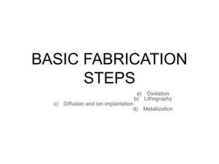
- 1. BASIC FABRICATION STEPS a) Oxidation b) Lithography c) Diffusion and ion implantation d) Metallization
- 2. Description 1) Oxidation: The development of high quality silicon dioxide(SiO2) has helped to establish the dominance of Si in the production of commercial ICs .Generally silicon dioxide functions as an insulator In a number of device structures or as a Barrier to diffusion or implantation in device fabrication. In fabrication of p-n junction the SiO2 film is used to define the junction area. There are two Sio2 growth methods,dry and wet oxidation. Fig:silicon Dioxide
- 3. 2) Lithography Another technology called photolithography is used to define the geometry of the P-N junction.After the formation of SiO2 wafer it is coted with an ultraviolet light sensitive material called photoresist.Which is spun on the surface of the wafer with a high speed spinner.
- 4. 3)Diffusion and Ion implantation In the diffusion process the semiconductor surface not protected by the oxide is exposed to a source with a high concentration of opposite type impurity.the impurity moves to the surface of the semiconductor crystal by solid state diffusion. In the Ion implantation method ,the intended impurity is introduced into the semiconductor by accelerating the impurity ions to a high energy level.
- 5. 4) Metallization After the Ion implantation process the mettalization process is continued toi form Ohmic contacts and interconnections.Metal film can be formed vby physical vapour deposition and chemical vapour deposition.with the completion of the metallization the P-N junction becomes functional.