SlideShare ist ein Scribd-Unternehmen logo
1 von 26
DESIGN OF VOLTAGE
CONTROLLED OSCILLATOR
(LOW POWER CONSUMPTION AND LOW PHASE NOISE)
1
Group No.28 Supervised By-
Saurabh Kumar Mr.Navaid Zafar Rizvi
Vaibhav Jindal
Sharad Sharma
CONTENT
• Motivation.
• Introduction.
• Design of VCO.
• Basic parameters of VCO.
• Base Paper.
• Objective.
• Tool Used.
• Design Implemented.
• Results Achieved.
• Future Work & Time Plan.
• References. 2
3
MOTIVATION
• Now a days communication is most necessary thing in
the world.
• Our aim is to make communication device of low
cost, less power consuming and Noise free.
• As Voltage Controlled Oscillator is used on both ends
of Communication.
• Or, we are trying to design a Voltage controlled
Oscillator which Consumed less power and having a
low phase noise
4
INTRODUCTION
• A voltage controlled oscillator is a device that
provides a varying output signal whose frequency
can be adjusted over the range controlled by D.C.
voltage
Voltage Controlled
Oscillator
Vcont ωout
Specifications of Ideal Voltage Controlled Oscillator
1. VCO is of Low Noise.
2. Low Power Consumption.
3. High Packing Density.
4. High Frequency.
5. Wide tuning range.
5
VOLTAGE CONTROLLED OSCILLATOR
• Noise is injected into an oscillator will disturb both
the amplitude and frequency of oscillation.
• Amplitude noise is usually unimportant but Phase
noise, on the other hand, is essentially a random
deviation in frequency which can also be viewed as a
random variation in the zero crossing points of the
time-dependent oscillator waveform.
.
6
OSCILLATOR PHASE NOISE
7
• Ring Oscillator Topology
• Relaxation Oscillator Topology
• Advantages-
Easy to fabricate
Low power
Small dice area occupancy
Wide tuning range.
• Disadvantage-
As frequency increases phase
noise performance degrades.
• LC Tank Oscillator Topology
• Crystal Oscillator Topology
• Advantages-
Low phase noise performance at
high frequency.
• Disadvantage-
Not suitable in fabrication
High power consumption
Small tuning range
Wave form Oscillators Resonant Oscillators
DIFFERENT OSCILLATORS DESIGN
• In this Topology oscillation frequency is decided by
L and C used in tank circuit of oscillator.
• Oscillation Frequency fosc =
• Only Inductor and Capacitor value has to vary
oscillation frequency.
• It is not easy to vary the value of L in monolithic
inductor, but we can change C by using Voltage
dependent capacitor (varactors).
8
LC OSCILLATOR TANK TOPOLOGY
• “Layout Design of LC VCO with Current Mirror Using 0.18
μm Technology”
• Namrata Prasad and Radheshyam Gamad
• Department of Electronics & Instrumentation Engineering, Shri
G. S. Institute of Technology and Science, Indore, India.
• Presented in Scientific Research Journal on Wireless
Engineering and Technology, in 2011.
• This paper presents a new design of complementary metal oxide
semiconductor voltage controlled oscillator (CMOS VCO) for
improve tuning range and phase noise with low power
consumption. 9
BASE PAPER
Our objective is to implement our Base paper
first in 180nm technology and then in 45nm
technology, and to achieve results better than our
base paper i.e. lower phase noise. We will
accomplish this task by designing an efficient
layout which requires less metal contacts.
10
OBJECTIVE
• Cadence Virtuoso.
• It is a Circuit simulator tool which provides capabilities of
designing the circuit, testing of circuit, designing of
layout and its verification.
• It has a feature named Analog Design Environment
(ADE).
• It also support tools like ASSURA, CALIBAR, ICE and
with the help of these tools we can have different checks
on our schematic like DRC, LVS.
11
TOOL USED
12
VCO DESIGN STEPS IN TOOL
• According to designing parameters add a predefine
library(gpdk180& gpdk45) to project
• Design a schematic
Made a symbol for schematic.
• Testing and Verification
Draw a test circuit schematic.
Simulation
Analysis of Phase noise
• Layout Design
Testing and verification
• Easy to learn and enter data.
• Simulation set-ups can be reused.
• Quick analysis of multiple simulation data.
• Cross probing support for both schematics and layouts.
• Multiple measurement syntaxes supported.
• Batch scripting waveform display.
• Supports multiple Y-axes, strip plots, and Smith Charts.
• Built-in waveform calculator.
13
FEATURES OF VIRTUOSO
• Design aims at minimizing the phase noise of oscillator
circuit.
• Circuit is a combination of both cross coupled VCO and
balanced VCO.
• Due to the combination of two configuration and a LC tank
circuit it produces lower phase noise.
• This configuration also helps in reducing the chip size.
• Power consumption is minimized by using two different
current mirrors.
14
VOLTAGE CONTROLLED OSCILLATOR DESIGN
15
VOLTAGE CONTROLLED OSCILLATOR DESIGN
• In first VCO Schematic-
Using Current Source
Tail has large Capacitance
• In Second VCO Schematic-
Using NMOS
Tail Current Source has a
noise at 2ω0
• In Third VCO Schematic-
Using Current Mirror
No large Capacitance
16
180 nm VCO Schematic
4 N-MOS
4 P-MOS
3 1pF Capacitors
1 1nH Inductor
17
VCO TEST CIRCUIT
18
SIMULATION RESULTS
19
SIMULATION RESULTS(POWER CONSUMPTION)
Calculated Power Is
4.708*10-3
20
SIMULATION RESULTS(PHASE NOISE)
21
SIMULATION RESULTS COMPARE WITH BASE PAPER
Parameters Namrata Prasad et al Proposed VCO
Results
General VCO
(Without current
mirror)
Propose VCO
(With current
mirror)
(VCO with
Current
Mirror)
Operating Voltage 2V 2V 2V
Technology(CMOS) 0.18um 0.18um 0.18um
Power Consumption 12.72mW 7.40mW 4.7mW
Operating Frequency 3.3GHz 3.3GHz 3.3GHz
Phase Noise (dBc/Hz) 63.7 at 100MHz -155.78 at 100MHz -128 at 1MHz
Phase Margin 180 180 180
22
LAYOUT
• Layout implementation of present 180nm circuit using
minimum possible metal contacts, which will help in
reducing power loss.
• Designing of schematic and test circuit of present
circuitry in 45nm technology and performing test
analyses.
• Layout implementation in 45nm technology.
• Performing Power and Noise analyses of the circuits.
23
FUTURE WORK
• Completion of 180nm design---> 1st week of April
• Completion of 45nm design ---> 3rd week of April
• Completion of final Analyses ---> 4th week of April
24
TIME PLAN
• Namrata Prasad and Radheshyam Gamad, “Layout
Design of LC VCO with Current Mirror Using 0.18 ÎĽm
Technology”, Scientific Research Journal on Wireless
Engineering and Technology, 2011.
• N. Prasad, R. S. Gamad and C. B. Kushwah, “Design of a
2.2 - 4.0 GHz Low Phase Noise and Low Power LC
VCO,” International Journal of Computer and
Network Security, 2009.
• B. Razavi, “Deign of Analog Complementary MOS
Integrated Circuits, Edition 3” Tata McGraw-
Hill, Delhi, 2002.
• P. Dudulwar, K. Shah, H. Le and J. Singh, “Design and
Analysis of Low Power Low Phase Noise VCO,” 13th
IEEE International Conference on Mixed Design of
Integrated Circuits and Systems,2006.
25
REFRENCES
Thank You
? ? ?
26

Weitere ähnliche Inhalte

Was ist angesagt?

Presentation on Op-amp by Sourabh kumar
Presentation on Op-amp by Sourabh kumarPresentation on Op-amp by Sourabh kumar
Presentation on Op-amp by Sourabh kumarSourabh Kumar
 
Double Side band Suppressed carrier (DSB-SC) Modulation and Demodulation.
 Double Side band Suppressed carrier (DSB-SC) Modulation and Demodulation. Double Side band Suppressed carrier (DSB-SC) Modulation and Demodulation.
Double Side band Suppressed carrier (DSB-SC) Modulation and Demodulation.SAiFul IslAm
 
waveshaping ckts
 waveshaping ckts waveshaping ckts
waveshaping cktsvishal gupta
 
Frequency-Shift Keying
Frequency-Shift KeyingFrequency-Shift Keying
Frequency-Shift KeyingJessie Rama
 
What is 16 qam modulation
What is 16 qam modulationWhat is 16 qam modulation
What is 16 qam modulationFOSCO Fiber Optics
 
Ch1 transistor as small signal amplifier
Ch1   transistor as small signal amplifierCh1   transistor as small signal amplifier
Ch1 transistor as small signal amplifierNorlaili MSafri
 
Rf power amplifier design
Rf power amplifier designRf power amplifier design
Rf power amplifier designvenkateshp100
 
S parameters
S parametersS parameters
S parametersAmit Rastogi
 
Timing issues in digital circuits
Timing issues in digital circuitsTiming issues in digital circuits
Timing issues in digital circuitsaroosa khan
 
Theory Communication
Theory CommunicationTheory Communication
Theory CommunicationHikari Riten
 
Schmitt trigger circuit
Schmitt trigger circuitSchmitt trigger circuit
Schmitt trigger circuittaranjeet10
 

Was ist angesagt? (20)

Presentation on Op-amp by Sourabh kumar
Presentation on Op-amp by Sourabh kumarPresentation on Op-amp by Sourabh kumar
Presentation on Op-amp by Sourabh kumar
 
Op amp
Op ampOp amp
Op amp
 
Double Side band Suppressed carrier (DSB-SC) Modulation and Demodulation.
 Double Side band Suppressed carrier (DSB-SC) Modulation and Demodulation. Double Side band Suppressed carrier (DSB-SC) Modulation and Demodulation.
Double Side band Suppressed carrier (DSB-SC) Modulation and Demodulation.
 
Generation of fm
Generation of fmGeneration of fm
Generation of fm
 
Phase locked loop
Phase locked loopPhase locked loop
Phase locked loop
 
waveshaping ckts
 waveshaping ckts waveshaping ckts
waveshaping ckts
 
Current mirror
Current mirrorCurrent mirror
Current mirror
 
Frequency-Shift Keying
Frequency-Shift KeyingFrequency-Shift Keying
Frequency-Shift Keying
 
What is 16 qam modulation
What is 16 qam modulationWhat is 16 qam modulation
What is 16 qam modulation
 
Ch1 transistor as small signal amplifier
Ch1   transistor as small signal amplifierCh1   transistor as small signal amplifier
Ch1 transistor as small signal amplifier
 
MOSFET....complete PPT
MOSFET....complete PPTMOSFET....complete PPT
MOSFET....complete PPT
 
Rf power amplifier design
Rf power amplifier designRf power amplifier design
Rf power amplifier design
 
Vlsi design notes
Vlsi design notesVlsi design notes
Vlsi design notes
 
S parameters
S parametersS parameters
S parameters
 
current mirrors
current mirrorscurrent mirrors
current mirrors
 
Unit v waveform generators
Unit v   waveform generatorsUnit v   waveform generators
Unit v waveform generators
 
Timing issues in digital circuits
Timing issues in digital circuitsTiming issues in digital circuits
Timing issues in digital circuits
 
Theory Communication
Theory CommunicationTheory Communication
Theory Communication
 
Schmitt trigger circuit
Schmitt trigger circuitSchmitt trigger circuit
Schmitt trigger circuit
 
Line coding
Line coding Line coding
Line coding
 

Andere mochten auch

Phase locked loop
Phase locked loop Phase locked loop
Phase locked loop imengineer
 
Phase lock loop (pll)
Phase lock loop (pll)Phase lock loop (pll)
Phase lock loop (pll)sulaim_qais
 
Phase locked loop design
Phase locked loop designPhase locked loop design
Phase locked loop designMoin Aman
 
c[Nemko]us - il Marchio Nemko per Canada e Nord America
c[Nemko]us - il Marchio Nemko per Canada e Nord America c[Nemko]us - il Marchio Nemko per Canada e Nord America
c[Nemko]us - il Marchio Nemko per Canada e Nord America Nemko Italy
 
Digital communication (DSSS)
Digital communication  (DSSS)Digital communication  (DSSS)
Digital communication (DSSS)SSGMCE SHEGAON
 
Dsss final
Dsss finalDsss final
Dsss finalAJAL A J
 
RF Module Design - [Chapter 7] Voltage-Controlled Oscillator
RF Module Design - [Chapter 7] Voltage-Controlled OscillatorRF Module Design - [Chapter 7] Voltage-Controlled Oscillator
RF Module Design - [Chapter 7] Voltage-Controlled OscillatorSimen Li
 
Op amp applications filters cw final
Op amp applications filters cw finalOp amp applications filters cw final
Op amp applications filters cw finalJUNAID SK
 
7.Active Filters using Opamp
7.Active Filters using Opamp7.Active Filters using Opamp
7.Active Filters using OpampINDIAN NAVY
 
Introduction to pll
Introduction to pllIntroduction to pll
Introduction to pllsartaj ahmed
 
Phase-locked Loops - Theory and Design
Phase-locked Loops - Theory and DesignPhase-locked Loops - Theory and Design
Phase-locked Loops - Theory and DesignSimen Li
 

Andere mochten auch (19)

Phase locked loop
Phase locked loop Phase locked loop
Phase locked loop
 
Pll
PllPll
Pll
 
Phase lock loop (pll)
Phase lock loop (pll)Phase lock loop (pll)
Phase lock loop (pll)
 
Phase locked loop design
Phase locked loop designPhase locked loop design
Phase locked loop design
 
Oscillators
OscillatorsOscillators
Oscillators
 
PHASE LOCK LOOPs
PHASE LOCK LOOPsPHASE LOCK LOOPs
PHASE LOCK LOOPs
 
RF-Microwave PCB
RF-Microwave PCBRF-Microwave PCB
RF-Microwave PCB
 
c[Nemko]us - il Marchio Nemko per Canada e Nord America
c[Nemko]us - il Marchio Nemko per Canada e Nord America c[Nemko]us - il Marchio Nemko per Canada e Nord America
c[Nemko]us - il Marchio Nemko per Canada e Nord America
 
Phase noise
Phase noisePhase noise
Phase noise
 
Digital communication (DSSS)
Digital communication  (DSSS)Digital communication  (DSSS)
Digital communication (DSSS)
 
Dsss final
Dsss finalDsss final
Dsss final
 
RF Module Design - [Chapter 7] Voltage-Controlled Oscillator
RF Module Design - [Chapter 7] Voltage-Controlled OscillatorRF Module Design - [Chapter 7] Voltage-Controlled Oscillator
RF Module Design - [Chapter 7] Voltage-Controlled Oscillator
 
Op amp applications filters cw final
Op amp applications filters cw finalOp amp applications filters cw final
Op amp applications filters cw final
 
Ea3
Ea3Ea3
Ea3
 
Pll Basic
Pll BasicPll Basic
Pll Basic
 
7.Active Filters using Opamp
7.Active Filters using Opamp7.Active Filters using Opamp
7.Active Filters using Opamp
 
Introduction to pll
Introduction to pllIntroduction to pll
Introduction to pll
 
Oscillatorsppt
OscillatorspptOscillatorsppt
Oscillatorsppt
 
Phase-locked Loops - Theory and Design
Phase-locked Loops - Theory and DesignPhase-locked Loops - Theory and Design
Phase-locked Loops - Theory and Design
 

Ă„hnlich wie design and analysis of voltage controlled oscillator

Professional Profile
Professional ProfileProfessional Profile
Professional Profilessramz
 
HC24.29.625-IA-23-Wide-Ruhl-Intel_2012_NTV_iA
HC24.29.625-IA-23-Wide-Ruhl-Intel_2012_NTV_iAHC24.29.625-IA-23-Wide-Ruhl-Intel_2012_NTV_iA
HC24.29.625-IA-23-Wide-Ruhl-Intel_2012_NTV_iASaurabh Dighe
 
12-edicon20185G Designing a Narrowband 28 GHz Band Pass Filter.pdf
12-edicon20185G Designing a Narrowband 28 GHz Band Pass Filter.pdf12-edicon20185G Designing a Narrowband 28 GHz Band Pass Filter.pdf
12-edicon20185G Designing a Narrowband 28 GHz Band Pass Filter.pdfessedikiftene
 
Devyani 1st Ext. Presentation
Devyani 1st Ext. PresentationDevyani 1st Ext. Presentation
Devyani 1st Ext. PresentationDevyani Balyan
 
Design of Energy- and Area-Efficient Sensor Readout Circuits (Chih-Chan Tu)
Design of Energy- and Area-Efficient Sensor Readout Circuits (Chih-Chan Tu)Design of Energy- and Area-Efficient Sensor Readout Circuits (Chih-Chan Tu)
Design of Energy- and Area-Efficient Sensor Readout Circuits (Chih-Chan Tu)Chih-Chan Tu
 
wireless charging of an electrical vechicle
wireless charging of an electrical vechiclewireless charging of an electrical vechicle
wireless charging of an electrical vechiclehari prasad
 
IBIS MODELING FOR WIDEBAND EMC APPLICATIONS
IBIS MODELING FOR WIDEBAND EMC APPLICATIONSIBIS MODELING FOR WIDEBAND EMC APPLICATIONS
IBIS MODELING FOR WIDEBAND EMC APPLICATIONSPiero Belforte
 
Team2_Presentation_ECE6414_S16
Team2_Presentation_ECE6414_S16Team2_Presentation_ECE6414_S16
Team2_Presentation_ECE6414_S16Tianhao Li
 
AMAR_KANTETI_RESUME
AMAR_KANTETI_RESUMEAMAR_KANTETI_RESUME
AMAR_KANTETI_RESUMEamar kanteti
 
Design of -- Two phase non overlapping low frequency clock generator using Ca...
Design of -- Two phase non overlapping low frequency clock generator using Ca...Design of -- Two phase non overlapping low frequency clock generator using Ca...
Design of -- Two phase non overlapping low frequency clock generator using Ca...Prashantkumar R
 
IRJET- Design and Implementation of High Speed, Low Power Charge Shared R...
IRJET-  	  Design and Implementation of High Speed, Low Power Charge Shared R...IRJET-  	  Design and Implementation of High Speed, Low Power Charge Shared R...
IRJET- Design and Implementation of High Speed, Low Power Charge Shared R...IRJET Journal
 
Low power in vlsi with upf basics part 1
Low power in vlsi with upf basics part 1Low power in vlsi with upf basics part 1
Low power in vlsi with upf basics part 1SUNODH GARLAPATI
 
Design and performance analysis of low phase noise LC-voltage controlled osci...
Design and performance analysis of low phase noise LC-voltage controlled osci...Design and performance analysis of low phase noise LC-voltage controlled osci...
Design and performance analysis of low phase noise LC-voltage controlled osci...TELKOMNIKA JOURNAL
 
3 phase energy meter on Zigbee1
3 phase energy meter on Zigbee13 phase energy meter on Zigbee1
3 phase energy meter on Zigbee1Sumit Vyas
 
Design of a 45nm TIQ Comparator for High Speed and Low Power 4-Bit Flash ADC
Design of a 45nm TIQ Comparator for High Speed and Low Power 4-Bit Flash ADCDesign of a 45nm TIQ Comparator for High Speed and Low Power 4-Bit Flash ADC
Design of a 45nm TIQ Comparator for High Speed and Low Power 4-Bit Flash ADCIDES Editor
 
An Ultra-Low Power Asynchronous-Logic
An Ultra-Low Power Asynchronous-LogicAn Ultra-Low Power Asynchronous-Logic
An Ultra-Low Power Asynchronous-LogicHossam Hassan
 
shravani_UGC.pdf eferhgtrjtyj hgfdhrtsgsdgse
shravani_UGC.pdf eferhgtrjtyj hgfdhrtsgsdgseshravani_UGC.pdf eferhgtrjtyj hgfdhrtsgsdgse
shravani_UGC.pdf eferhgtrjtyj hgfdhrtsgsdgsepankajrangaree2
 

Ă„hnlich wie design and analysis of voltage controlled oscillator (20)

Professional Profile
Professional ProfileProfessional Profile
Professional Profile
 
HC24.29.625-IA-23-Wide-Ruhl-Intel_2012_NTV_iA
HC24.29.625-IA-23-Wide-Ruhl-Intel_2012_NTV_iAHC24.29.625-IA-23-Wide-Ruhl-Intel_2012_NTV_iA
HC24.29.625-IA-23-Wide-Ruhl-Intel_2012_NTV_iA
 
12-edicon20185G Designing a Narrowband 28 GHz Band Pass Filter.pdf
12-edicon20185G Designing a Narrowband 28 GHz Band Pass Filter.pdf12-edicon20185G Designing a Narrowband 28 GHz Band Pass Filter.pdf
12-edicon20185G Designing a Narrowband 28 GHz Band Pass Filter.pdf
 
Devyani 1st Ext. Presentation
Devyani 1st Ext. PresentationDevyani 1st Ext. Presentation
Devyani 1st Ext. Presentation
 
Design of Energy- and Area-Efficient Sensor Readout Circuits (Chih-Chan Tu)
Design of Energy- and Area-Efficient Sensor Readout Circuits (Chih-Chan Tu)Design of Energy- and Area-Efficient Sensor Readout Circuits (Chih-Chan Tu)
Design of Energy- and Area-Efficient Sensor Readout Circuits (Chih-Chan Tu)
 
wireless charging of an electrical vechicle
wireless charging of an electrical vechiclewireless charging of an electrical vechicle
wireless charging of an electrical vechicle
 
IBIS MODELING FOR WIDEBAND EMC APPLICATIONS
IBIS MODELING FOR WIDEBAND EMC APPLICATIONSIBIS MODELING FOR WIDEBAND EMC APPLICATIONS
IBIS MODELING FOR WIDEBAND EMC APPLICATIONS
 
Team2_Presentation_ECE6414_S16
Team2_Presentation_ECE6414_S16Team2_Presentation_ECE6414_S16
Team2_Presentation_ECE6414_S16
 
AMAR_KANTETI_RESUME
AMAR_KANTETI_RESUMEAMAR_KANTETI_RESUME
AMAR_KANTETI_RESUME
 
Design of -- Two phase non overlapping low frequency clock generator using Ca...
Design of -- Two phase non overlapping low frequency clock generator using Ca...Design of -- Two phase non overlapping low frequency clock generator using Ca...
Design of -- Two phase non overlapping low frequency clock generator using Ca...
 
IRJET- Design and Implementation of High Speed, Low Power Charge Shared R...
IRJET-  	  Design and Implementation of High Speed, Low Power Charge Shared R...IRJET-  	  Design and Implementation of High Speed, Low Power Charge Shared R...
IRJET- Design and Implementation of High Speed, Low Power Charge Shared R...
 
Low power in vlsi with upf basics part 1
Low power in vlsi with upf basics part 1Low power in vlsi with upf basics part 1
Low power in vlsi with upf basics part 1
 
Design and performance analysis of low phase noise LC-voltage controlled osci...
Design and performance analysis of low phase noise LC-voltage controlled osci...Design and performance analysis of low phase noise LC-voltage controlled osci...
Design and performance analysis of low phase noise LC-voltage controlled osci...
 
rcwire.ppt
rcwire.pptrcwire.ppt
rcwire.ppt
 
3 phase energy meter on Zigbee1
3 phase energy meter on Zigbee13 phase energy meter on Zigbee1
3 phase energy meter on Zigbee1
 
Design of a 45nm TIQ Comparator for High Speed and Low Power 4-Bit Flash ADC
Design of a 45nm TIQ Comparator for High Speed and Low Power 4-Bit Flash ADCDesign of a 45nm TIQ Comparator for High Speed and Low Power 4-Bit Flash ADC
Design of a 45nm TIQ Comparator for High Speed and Low Power 4-Bit Flash ADC
 
ICIECA 2014 Paper 23
ICIECA 2014 Paper 23ICIECA 2014 Paper 23
ICIECA 2014 Paper 23
 
An Ultra-Low Power Asynchronous-Logic
An Ultra-Low Power Asynchronous-LogicAn Ultra-Low Power Asynchronous-Logic
An Ultra-Low Power Asynchronous-Logic
 
Bt31482484
Bt31482484Bt31482484
Bt31482484
 
shravani_UGC.pdf eferhgtrjtyj hgfdhrtsgsdgse
shravani_UGC.pdf eferhgtrjtyj hgfdhrtsgsdgseshravani_UGC.pdf eferhgtrjtyj hgfdhrtsgsdgse
shravani_UGC.pdf eferhgtrjtyj hgfdhrtsgsdgse
 

Mehr von vaibhav jindal

Ammeter&voltmeter
Ammeter&voltmeterAmmeter&voltmeter
Ammeter&voltmetervaibhav jindal
 
Hay's bridge phasor diagram draw
Hay's bridge phasor diagram drawHay's bridge phasor diagram draw
Hay's bridge phasor diagram drawvaibhav jindal
 
Basics of Computer hardware and Software
Basics of Computer hardware and SoftwareBasics of Computer hardware and Software
Basics of Computer hardware and Softwarevaibhav jindal
 
Layout design on MICROWIND
Layout design on MICROWINDLayout design on MICROWIND
Layout design on MICROWINDvaibhav jindal
 
Circuit on bread board
Circuit on bread boardCircuit on bread board
Circuit on bread boardvaibhav jindal
 
Stability of Control System
Stability of Control SystemStability of Control System
Stability of Control Systemvaibhav jindal
 
Basic Electronics components
Basic Electronics componentsBasic Electronics components
Basic Electronics componentsvaibhav jindal
 
Auto dial-er Home security
Auto dial-er Home securityAuto dial-er Home security
Auto dial-er Home securityvaibhav jindal
 
Buffer op amplifier
Buffer op amplifierBuffer op amplifier
Buffer op amplifiervaibhav jindal
 
Fabrication of passive elements
Fabrication of passive elementsFabrication of passive elements
Fabrication of passive elementsvaibhav jindal
 
Fabrication of passive elements
Fabrication of passive elementsFabrication of passive elements
Fabrication of passive elementsvaibhav jindal
 

Mehr von vaibhav jindal (16)

Ammeter&voltmeter
Ammeter&voltmeterAmmeter&voltmeter
Ammeter&voltmeter
 
Hay's bridge phasor diagram draw
Hay's bridge phasor diagram drawHay's bridge phasor diagram draw
Hay's bridge phasor diagram draw
 
Voltmeter
VoltmeterVoltmeter
Voltmeter
 
Basics of Computer hardware and Software
Basics of Computer hardware and SoftwareBasics of Computer hardware and Software
Basics of Computer hardware and Software
 
Layout design on MICROWIND
Layout design on MICROWINDLayout design on MICROWIND
Layout design on MICROWIND
 
Circuit on bread board
Circuit on bread boardCircuit on bread board
Circuit on bread board
 
Stability of Control System
Stability of Control SystemStability of Control System
Stability of Control System
 
Basic Electronics components
Basic Electronics componentsBasic Electronics components
Basic Electronics components
 
Vedic
VedicVedic
Vedic
 
Auto dial-er Home security
Auto dial-er Home securityAuto dial-er Home security
Auto dial-er Home security
 
Gailtel
GailtelGailtel
Gailtel
 
Ppt final (1)
Ppt final (1)Ppt final (1)
Ppt final (1)
 
Vaibhav (2)
Vaibhav (2)Vaibhav (2)
Vaibhav (2)
 
Buffer op amplifier
Buffer op amplifierBuffer op amplifier
Buffer op amplifier
 
Fabrication of passive elements
Fabrication of passive elementsFabrication of passive elements
Fabrication of passive elements
 
Fabrication of passive elements
Fabrication of passive elementsFabrication of passive elements
Fabrication of passive elements
 

KĂĽrzlich hochgeladen

Sanyam Choudhary Chemistry practical.pdf
Sanyam Choudhary Chemistry practical.pdfSanyam Choudhary Chemistry practical.pdf
Sanyam Choudhary Chemistry practical.pdfsanyamsingh5019
 
mini mental status format.docx
mini    mental       status     format.docxmini    mental       status     format.docx
mini mental status format.docxPoojaSen20
 
Mastering the Unannounced Regulatory Inspection
Mastering the Unannounced Regulatory InspectionMastering the Unannounced Regulatory Inspection
Mastering the Unannounced Regulatory InspectionSafetyChain Software
 
APM Welcome, APM North West Network Conference, Synergies Across Sectors
APM Welcome, APM North West Network Conference, Synergies Across SectorsAPM Welcome, APM North West Network Conference, Synergies Across Sectors
APM Welcome, APM North West Network Conference, Synergies Across SectorsAssociation for Project Management
 
Micromeritics - Fundamental and Derived Properties of Powders
Micromeritics - Fundamental and Derived Properties of PowdersMicromeritics - Fundamental and Derived Properties of Powders
Micromeritics - Fundamental and Derived Properties of PowdersChitralekhaTherkar
 
BASLIQ CURRENT LOOKBOOK LOOKBOOK(1) (1).pdf
BASLIQ CURRENT LOOKBOOK  LOOKBOOK(1) (1).pdfBASLIQ CURRENT LOOKBOOK  LOOKBOOK(1) (1).pdf
BASLIQ CURRENT LOOKBOOK LOOKBOOK(1) (1).pdfSoniaTolstoy
 
Kisan Call Centre - To harness potential of ICT in Agriculture by answer farm...
Kisan Call Centre - To harness potential of ICT in Agriculture by answer farm...Kisan Call Centre - To harness potential of ICT in Agriculture by answer farm...
Kisan Call Centre - To harness potential of ICT in Agriculture by answer farm...Krashi Coaching
 
Solving Puzzles Benefits Everyone (English).pptx
Solving Puzzles Benefits Everyone (English).pptxSolving Puzzles Benefits Everyone (English).pptx
Solving Puzzles Benefits Everyone (English).pptxOH TEIK BIN
 
Crayon Activity Handout For the Crayon A
Crayon Activity Handout For the Crayon ACrayon Activity Handout For the Crayon A
Crayon Activity Handout For the Crayon AUnboundStockton
 
Science 7 - LAND and SEA BREEZE and its Characteristics
Science 7 - LAND and SEA BREEZE and its CharacteristicsScience 7 - LAND and SEA BREEZE and its Characteristics
Science 7 - LAND and SEA BREEZE and its CharacteristicsKarinaGenton
 
Software Engineering Methodologies (overview)
Software Engineering Methodologies (overview)Software Engineering Methodologies (overview)
Software Engineering Methodologies (overview)eniolaolutunde
 
MENTAL STATUS EXAMINATION format.docx
MENTAL     STATUS EXAMINATION format.docxMENTAL     STATUS EXAMINATION format.docx
MENTAL STATUS EXAMINATION format.docxPoojaSen20
 
Presiding Officer Training module 2024 lok sabha elections
Presiding Officer Training module 2024 lok sabha electionsPresiding Officer Training module 2024 lok sabha elections
Presiding Officer Training module 2024 lok sabha electionsanshu789521
 
The basics of sentences session 2pptx copy.pptx
The basics of sentences session 2pptx copy.pptxThe basics of sentences session 2pptx copy.pptx
The basics of sentences session 2pptx copy.pptxheathfieldcps1
 
Contemporary philippine arts from the regions_PPT_Module_12 [Autosaved] (1).pptx
Contemporary philippine arts from the regions_PPT_Module_12 [Autosaved] (1).pptxContemporary philippine arts from the regions_PPT_Module_12 [Autosaved] (1).pptx
Contemporary philippine arts from the regions_PPT_Module_12 [Autosaved] (1).pptxRoyAbrique
 
microwave assisted reaction. General introduction
microwave assisted reaction. General introductionmicrowave assisted reaction. General introduction
microwave assisted reaction. General introductionMaksud Ahmed
 
Paris 2024 Olympic Geographies - an activity
Paris 2024 Olympic Geographies - an activityParis 2024 Olympic Geographies - an activity
Paris 2024 Olympic Geographies - an activityGeoBlogs
 
Concept of Vouching. B.Com(Hons) /B.Compdf
Concept of Vouching. B.Com(Hons) /B.CompdfConcept of Vouching. B.Com(Hons) /B.Compdf
Concept of Vouching. B.Com(Hons) /B.CompdfUmakantAnnand
 
Arihant handbook biology for class 11 .pdf
Arihant handbook biology for class 11 .pdfArihant handbook biology for class 11 .pdf
Arihant handbook biology for class 11 .pdfchloefrazer622
 

KĂĽrzlich hochgeladen (20)

Sanyam Choudhary Chemistry practical.pdf
Sanyam Choudhary Chemistry practical.pdfSanyam Choudhary Chemistry practical.pdf
Sanyam Choudhary Chemistry practical.pdf
 
mini mental status format.docx
mini    mental       status     format.docxmini    mental       status     format.docx
mini mental status format.docx
 
Mastering the Unannounced Regulatory Inspection
Mastering the Unannounced Regulatory InspectionMastering the Unannounced Regulatory Inspection
Mastering the Unannounced Regulatory Inspection
 
APM Welcome, APM North West Network Conference, Synergies Across Sectors
APM Welcome, APM North West Network Conference, Synergies Across SectorsAPM Welcome, APM North West Network Conference, Synergies Across Sectors
APM Welcome, APM North West Network Conference, Synergies Across Sectors
 
Micromeritics - Fundamental and Derived Properties of Powders
Micromeritics - Fundamental and Derived Properties of PowdersMicromeritics - Fundamental and Derived Properties of Powders
Micromeritics - Fundamental and Derived Properties of Powders
 
BASLIQ CURRENT LOOKBOOK LOOKBOOK(1) (1).pdf
BASLIQ CURRENT LOOKBOOK  LOOKBOOK(1) (1).pdfBASLIQ CURRENT LOOKBOOK  LOOKBOOK(1) (1).pdf
BASLIQ CURRENT LOOKBOOK LOOKBOOK(1) (1).pdf
 
Kisan Call Centre - To harness potential of ICT in Agriculture by answer farm...
Kisan Call Centre - To harness potential of ICT in Agriculture by answer farm...Kisan Call Centre - To harness potential of ICT in Agriculture by answer farm...
Kisan Call Centre - To harness potential of ICT in Agriculture by answer farm...
 
Solving Puzzles Benefits Everyone (English).pptx
Solving Puzzles Benefits Everyone (English).pptxSolving Puzzles Benefits Everyone (English).pptx
Solving Puzzles Benefits Everyone (English).pptx
 
Crayon Activity Handout For the Crayon A
Crayon Activity Handout For the Crayon ACrayon Activity Handout For the Crayon A
Crayon Activity Handout For the Crayon A
 
Science 7 - LAND and SEA BREEZE and its Characteristics
Science 7 - LAND and SEA BREEZE and its CharacteristicsScience 7 - LAND and SEA BREEZE and its Characteristics
Science 7 - LAND and SEA BREEZE and its Characteristics
 
Model Call Girl in Bikash Puri Delhi reach out to us at 🔝9953056974🔝
Model Call Girl in Bikash Puri  Delhi reach out to us at 🔝9953056974🔝Model Call Girl in Bikash Puri  Delhi reach out to us at 🔝9953056974🔝
Model Call Girl in Bikash Puri Delhi reach out to us at 🔝9953056974🔝
 
Software Engineering Methodologies (overview)
Software Engineering Methodologies (overview)Software Engineering Methodologies (overview)
Software Engineering Methodologies (overview)
 
MENTAL STATUS EXAMINATION format.docx
MENTAL     STATUS EXAMINATION format.docxMENTAL     STATUS EXAMINATION format.docx
MENTAL STATUS EXAMINATION format.docx
 
Presiding Officer Training module 2024 lok sabha elections
Presiding Officer Training module 2024 lok sabha electionsPresiding Officer Training module 2024 lok sabha elections
Presiding Officer Training module 2024 lok sabha elections
 
The basics of sentences session 2pptx copy.pptx
The basics of sentences session 2pptx copy.pptxThe basics of sentences session 2pptx copy.pptx
The basics of sentences session 2pptx copy.pptx
 
Contemporary philippine arts from the regions_PPT_Module_12 [Autosaved] (1).pptx
Contemporary philippine arts from the regions_PPT_Module_12 [Autosaved] (1).pptxContemporary philippine arts from the regions_PPT_Module_12 [Autosaved] (1).pptx
Contemporary philippine arts from the regions_PPT_Module_12 [Autosaved] (1).pptx
 
microwave assisted reaction. General introduction
microwave assisted reaction. General introductionmicrowave assisted reaction. General introduction
microwave assisted reaction. General introduction
 
Paris 2024 Olympic Geographies - an activity
Paris 2024 Olympic Geographies - an activityParis 2024 Olympic Geographies - an activity
Paris 2024 Olympic Geographies - an activity
 
Concept of Vouching. B.Com(Hons) /B.Compdf
Concept of Vouching. B.Com(Hons) /B.CompdfConcept of Vouching. B.Com(Hons) /B.Compdf
Concept of Vouching. B.Com(Hons) /B.Compdf
 
Arihant handbook biology for class 11 .pdf
Arihant handbook biology for class 11 .pdfArihant handbook biology for class 11 .pdf
Arihant handbook biology for class 11 .pdf
 

design and analysis of voltage controlled oscillator

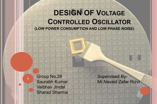
  • 1. DESIGN OF VOLTAGE CONTROLLED OSCILLATOR (LOW POWER CONSUMPTION AND LOW PHASE NOISE) 1 Group No.28 Supervised By- Saurabh Kumar Mr.Navaid Zafar Rizvi Vaibhav Jindal Sharad Sharma
  • 2. CONTENT • Motivation. • Introduction. • Design of VCO. • Basic parameters of VCO. • Base Paper. • Objective. • Tool Used. • Design Implemented. • Results Achieved. • Future Work & Time Plan. • References. 2
  • 3. 3 MOTIVATION • Now a days communication is most necessary thing in the world. • Our aim is to make communication device of low cost, less power consuming and Noise free. • As Voltage Controlled Oscillator is used on both ends of Communication. • Or, we are trying to design a Voltage controlled Oscillator which Consumed less power and having a low phase noise
  • 4. 4 INTRODUCTION • A voltage controlled oscillator is a device that provides a varying output signal whose frequency can be adjusted over the range controlled by D.C. voltage Voltage Controlled Oscillator Vcont ωout
  • 5. Specifications of Ideal Voltage Controlled Oscillator 1. VCO is of Low Noise. 2. Low Power Consumption. 3. High Packing Density. 4. High Frequency. 5. Wide tuning range. 5 VOLTAGE CONTROLLED OSCILLATOR
  • 6. • Noise is injected into an oscillator will disturb both the amplitude and frequency of oscillation. • Amplitude noise is usually unimportant but Phase noise, on the other hand, is essentially a random deviation in frequency which can also be viewed as a random variation in the zero crossing points of the time-dependent oscillator waveform. . 6 OSCILLATOR PHASE NOISE
  • 7. 7 • Ring Oscillator Topology • Relaxation Oscillator Topology • Advantages- Easy to fabricate Low power Small dice area occupancy Wide tuning range. • Disadvantage- As frequency increases phase noise performance degrades. • LC Tank Oscillator Topology • Crystal Oscillator Topology • Advantages- Low phase noise performance at high frequency. • Disadvantage- Not suitable in fabrication High power consumption Small tuning range Wave form Oscillators Resonant Oscillators DIFFERENT OSCILLATORS DESIGN
  • 8. • In this Topology oscillation frequency is decided by L and C used in tank circuit of oscillator. • Oscillation Frequency fosc = • Only Inductor and Capacitor value has to vary oscillation frequency. • It is not easy to vary the value of L in monolithic inductor, but we can change C by using Voltage dependent capacitor (varactors). 8 LC OSCILLATOR TANK TOPOLOGY
  • 9. • “Layout Design of LC VCO with Current Mirror Using 0.18 ÎĽm Technology” • Namrata Prasad and Radheshyam Gamad • Department of Electronics & Instrumentation Engineering, Shri G. S. Institute of Technology and Science, Indore, India. • Presented in Scientific Research Journal on Wireless Engineering and Technology, in 2011. • This paper presents a new design of complementary metal oxide semiconductor voltage controlled oscillator (CMOS VCO) for improve tuning range and phase noise with low power consumption. 9 BASE PAPER
  • 10. Our objective is to implement our Base paper first in 180nm technology and then in 45nm technology, and to achieve results better than our base paper i.e. lower phase noise. We will accomplish this task by designing an efficient layout which requires less metal contacts. 10 OBJECTIVE
  • 11. • Cadence Virtuoso. • It is a Circuit simulator tool which provides capabilities of designing the circuit, testing of circuit, designing of layout and its verification. • It has a feature named Analog Design Environment (ADE). • It also support tools like ASSURA, CALIBAR, ICE and with the help of these tools we can have different checks on our schematic like DRC, LVS. 11 TOOL USED
  • 12. 12 VCO DESIGN STEPS IN TOOL • According to designing parameters add a predefine library(gpdk180& gpdk45) to project • Design a schematic Made a symbol for schematic. • Testing and Verification Draw a test circuit schematic. Simulation Analysis of Phase noise • Layout Design Testing and verification
  • 13. • Easy to learn and enter data. • Simulation set-ups can be reused. • Quick analysis of multiple simulation data. • Cross probing support for both schematics and layouts. • Multiple measurement syntaxes supported. • Batch scripting waveform display. • Supports multiple Y-axes, strip plots, and Smith Charts. • Built-in waveform calculator. 13 FEATURES OF VIRTUOSO
  • 14. • Design aims at minimizing the phase noise of oscillator circuit. • Circuit is a combination of both cross coupled VCO and balanced VCO. • Due to the combination of two configuration and a LC tank circuit it produces lower phase noise. • This configuration also helps in reducing the chip size. • Power consumption is minimized by using two different current mirrors. 14 VOLTAGE CONTROLLED OSCILLATOR DESIGN
  • 15. 15 VOLTAGE CONTROLLED OSCILLATOR DESIGN • In first VCO Schematic- Using Current Source Tail has large Capacitance • In Second VCO Schematic- Using NMOS Tail Current Source has a noise at 2ω0 • In Third VCO Schematic- Using Current Mirror No large Capacitance
  • 16. 16 180 nm VCO Schematic 4 N-MOS 4 P-MOS 3 1pF Capacitors 1 1nH Inductor
  • 21. 21 SIMULATION RESULTS COMPARE WITH BASE PAPER Parameters Namrata Prasad et al Proposed VCO Results General VCO (Without current mirror) Propose VCO (With current mirror) (VCO with Current Mirror) Operating Voltage 2V 2V 2V Technology(CMOS) 0.18um 0.18um 0.18um Power Consumption 12.72mW 7.40mW 4.7mW Operating Frequency 3.3GHz 3.3GHz 3.3GHz Phase Noise (dBc/Hz) 63.7 at 100MHz -155.78 at 100MHz -128 at 1MHz Phase Margin 180 180 180
  • 23. • Layout implementation of present 180nm circuit using minimum possible metal contacts, which will help in reducing power loss. • Designing of schematic and test circuit of present circuitry in 45nm technology and performing test analyses. • Layout implementation in 45nm technology. • Performing Power and Noise analyses of the circuits. 23 FUTURE WORK
  • 24. • Completion of 180nm design---> 1st week of April • Completion of 45nm design ---> 3rd week of April • Completion of final Analyses ---> 4th week of April 24 TIME PLAN
  • 25. • Namrata Prasad and Radheshyam Gamad, “Layout Design of LC VCO with Current Mirror Using 0.18 ÎĽm Technology”, Scientific Research Journal on Wireless Engineering and Technology, 2011. • N. Prasad, R. S. Gamad and C. B. Kushwah, “Design of a 2.2 - 4.0 GHz Low Phase Noise and Low Power LC VCO,” International Journal of Computer and Network Security, 2009. • B. Razavi, “Deign of Analog Complementary MOS Integrated Circuits, Edition 3” Tata McGraw- Hill, Delhi, 2002. • P. Dudulwar, K. Shah, H. Le and J. Singh, “Design and Analysis of Low Power Low Phase Noise VCO,” 13th IEEE International Conference on Mixed Design of Integrated Circuits and Systems,2006. 25 REFRENCES

Hinweis der Redaktion

  1. Reversed pn junction can be served as varactor and voltage dependent is expressed as equationdepend on Co zero bias value,VR reversed bias voltage,built in potential