SlideShare ist ein Scribd-Unternehmen logo
1 von 80
P R E S E N T E D B Y : -
D R . G A U R A V S . S A L U N K H E
2 N D M D S
O R A L & M A X I L L O F A C I A L P A T H O L O G Y
SCANNING ELECTRON
MICROSCOPE
Contents
 Introduction
 History
 Construction of SEM
 Basics of specimen preparation
 Why images are visible
History
 The development of a SEM began a few yrs after the
invention of a TEM by Ruska in 1931, but the
commercialization of the SEM required about 30 yrs.
 In 1935, the original prototype of the SEM, which
scans the specimen with an e- beam to obtain an
image, was made by Knoll(Germany).
 In 1942, Zworykin (USA), developed a SEM for
observing a bulk specimens.
 In 1965, Cambridge Scientific Instrument
(UK) & JOEL (Japan) first commercialized
SEM individually.
Construction of SEM
A) Electron optical system.(to produce e-)
 electron gun, condenser lens, objective lens,
scanning coil.
B) Specimen stage (to place the specimen).
C) Secondary e- detector (to collect secondary e-).
D) Image display unit.
E) Operating system.
The electron optical system and a space surrounding
the specimen are kept at vacuum.
Construction of SEM
 Electron Gun- it produces an e- beam.
 It is a thermionic emission gun. (TEG), the thermo
electrons are emitted from a filament (cathode)
made of a thin tungsten wire, (about 0.1mm ) by
heating the filament at high temperature (about
2800k). Tungsten filament assembly
Construction of SEM
 These e- are gathered as an e-beam, flowing into the
metal plate (anode) by applying a positive voltage.
 If the hole is made at the center of the plate the e-
beam flows through this hole.
 If an electrode (Wehnelt electrode)is placed between
the cathode and anode and applied with the negative
charge, the speed of the e- beam can be adjusted.
Construction of SEM
 Condenser lens/Electromagnetic lens- placing a lens
below the e- gun enables to adjust the diameter of
the e- beam.
 A fine e- beam is requires for SEM .
A typical Electro Magnetic Lens
 Role of the condenser lens in formation of fine e-
beam
 The aperture is placed between the condenser lens
and objective lens.
 The aperture made of a thin metal plate, has a small
hole.
 The e- beam, which passed through the condenser
lens, illuminates this aperture-plate.
 The aperture allows a part of the e- beam to reach
the objective lens.
Construction of SEM
 If the excitation of the condenser lens is increased,
the e- beam greatly broadens on the aperture and
therefore the number of the electrons reaching the
objective lens decreases.
 To the contrary, if the excitation of the condenser
lens is decreased, the e- bean doesn’t broaden very
much and therefore, most of the electrons pass
through the aperture and many electrons reaches the
objective lens.
 In this way the e- probe diameter and the probe
current can be adjusted.
Construction of SEM
 Objective lens- the objective lens is used for focusing.
Construction of SEM
 Specimen stage- It supports the specimen.
 Moves smoothly.
 It can perform horizontal (x,y axis) & vertical
movements(z axis), tilting of specimen, and rotation.
 The horizontal movement is used for selection of the
field while the vertical movement is used to change
the image resolution.
SEM opened sample chamber
 Secondary e- detector- It is used for detecting the
secondary e- emitted from the specimen.
 A scintillator (fluorescent substance) is coated on the
tip of the detector and a high voltage of about 10 kV
is applied to it.
 The secondary e- are attracted to this high voltage
and then generate light when they hit the scintillator.
 This light is directed to a photon-multiplier tube
(PMT) through a light guide.
 The light is converted to the electrons, and these are
amplified as an electric signal.
Secondary electron
detector
Everhard -Thornley
Detector
 A supplementary electrode, called the collector, is
placed before the scintillator, and is applied with few
hundreds of voltage.
 This collector, helps the scintillator to acquire
secondary electrons.
 By changing the voltage the amount of secondary
electrons to be collected can be adjusted.
 This collector was originally developed by Everhart
and Thornley, so this detector can also be called as
E-T detector.
 When SEM is equipped with a strongly excited
objective lens for higher resolution a secondary
electron detector is placed above the objective lens.
 This type of detector is called TTL ie. (Through The
Lens ) detector.
 Image display unit- The out put signals from the
secondary electron detector are amplified and then
transferred to the display unit.
 Since the scanning on the display unit is
synchronized with the electron-probe scan,
brightness variation, which depends on the number
of the secondary electrons, appears on the monitor
screen on the display unit, thus forming a SEM
image.
 In general, the scan speed of the electron probe can
be changed in several steps.
 An extremely fast speed is used for observation and a
slow scan speed is used for saving of image.
 The image is recorded in a digital format (electrical
file), It is easier to process image and convenient to
send or receive image information.
 Vacuum system- The electron optical system and
the specimen chamber must be kept at a high
vacuum of 10-3 to 10-4 Pa.
 Thus , these component is evacuated by diffusion
pump. If a user desire an oil-free environment, a
turbo molecular pump may be used.
Sample Preparation
1. Cleaning the surface of the specimen.
2. Stabilizing the specimen.
3. Rinsing the specimen.
4. Dehydrating the specimen.
5. Drying the specimen.
6. Mounting the specimen.
7. Coating the specimen.
 Cleaning the surface of the specimen.
The proper cleaning of the surface of the specimen is
important, because the surface contains many
unwanted deposits, such as dust, mud, soil etc.
depending upon the source of the sample/specimen.
 Stabilizing the specimen.
 Hard, dry materials such as wood, bone, feathers, dried
insects, or shells can be examined with little further
treatment, but living cells and tissues and whole, soft-
bodied organisms usually require chemical fixation to
preserve and stabilize their structure.
 Stabilization is typically done with fixatives.
Fixation cab be achieved by :-
1. Perfusion or microinjection.
2. Immersions.
3. With vapours.
 Fixation is usually performed by incubation in a
solution of a buffered chemical fixative, such
as glutaraldehyde, sometimes in combination
with formaldehyde and other fixatives.
Fixatives that can be used are:-
1. Aldehydes.
2. Osmium tetroxide.
3. Tanic acid.
4. Thiocarbohydrazides.
 Rinsing the specimen.
After the fixation step, the sample must be rinsed in
order to remove excessive fixatives.
 Dehydrating the specimen.
 All water must be removed from the samples because
the water would vaporize in the vacuum.
 The fixed tissue is then dehydrated. Because air-
drying causes collapse and shrinkage, this is
commonly achieved by replacement of water in the
cells with organic solvents such
as ethanol or acetone.
 Dehydration is performed with a graded series of
ethanol or acetone.
 Drying the specimen.
 For SEM, a specimen is normally required to be
completely dry, since the specimen chamber is at
high vacuum.
 Otherwise the sample will be destroyed in the
electron microscope chamber.
 Mounting the specimen.
 After the specimen has been cleaned, fixed, rinsed,
dehydrated and dried, using an appropriate protocol,
specimen has to be mounted on the holder that can
be inserted into the scanning electron microscope.
 All samples must also be of an appropriate size to fit
in the specimen chamber and are generally mounted
rigidly on a specimen holder called a specimen stub.
 The dry specimen is usually mounted on a specimen
stub using an adhesive such as epoxy resin or
electrically conductive double-sided adhesive tape.
Charge-up
 This charge-up phenomenon can be prevented by
coating the non-conductor sample with metal
(conductor).
 Sample coating is
intended to prevent
charge-up phenomenon
by allowing the charge on
the specimen surface go
to ground through the
coated conductive film.
 Coating the specimen.
 The idea of coating the specimen is to increase the
conductivity of the specimen and to prevent the high
voltage charge on the specimen by conducting charge
to the ground.
 These specimen are coated with thin layer ie.20nm-
30nm of conductive metal.
 All metals are conductive and require no preparation
before being used.
 All non-metals need to be made conductive by
covering the sample with a thin layer of conductive
material.
 This is done by using a device called a "sputter
coater.”
 Conductive materials in current used for specimen
coating includes gold, gold-palladium alloy ,
platinum, osmium , iridium, tungsten, chromium
and graphite.
“Sputter Coater”
Advantages Disadvantages
1. Thermal conductivity is
increased.
2. Damaged to the sample
is reduced.
3. The quantity of
secondary electrons is
increased.
1. The shape & size of
nano particle is lost or
altered.
2. Specimen information
about elemental
composition & surface
potential may be lost.
Metal Coating
Why Images Are Visible?
 The SEM image appears as if it is been observed by
the naked eye.
 Interaction of electrons with specimens: when
e- enters the specimen, they are scattered with in the
specimen and gradually lose their energy.
 The scattering range of the electrons inside the
specimen is different depending on the electron
energy, atomic number, and the density of the
constituent atom.
 If the atomic number and density are larger, the
scattering range is smaller.
 If the electron energy is higher then the scattering
range is larger.
How Does SEM Works
 To further understand how does SEM works, we must
begin with the electrons. In a light microscope, light from
a source (usually an incandescent light) is focused
through lenses onto the sample. The image is
formed when the sample reflects and absorbs different
wavelengths of this light which is detected by our eyes
and formed into an image by our brains. An electron
microscope works in a similar fashion. Electrons from a
source are focused on the sample. These electrons reflect
off the sample, they are then picked up by an
electron detector and then processed into an
image which is projected onto a CRT that our eyes can
see.
 To begin our understanding of how an SEM works, let's
begin with the source of electrons, the electron gun.
 Most SEMs have what is called a hot cathode source,
usually a tungsten filament similar to that in a light bulb.
 When such a filament is heated by passing current
through it, it not only emits light, but an electron cloud
forms around the filament.
 Left on their own, they remain in the cloud and are
reabsorbed into the filament when the current is
removed.
 Placing a positively charged plate
(an anode) near the filament and
the electrons (being negatively
charged) will be attracted to it.
 Problem is, the electrons would
not be well directed and would
probably jump over to the anode
plate in a series of arcs.
 But by placing a negatively charged
cathode plate near the filament
(which they are repelled by) with a
hole in it and a positively charged
anode (which they are attracted to)
under this with another hole in it
and we have the makings of an
electron gun.
 The electron cloud is attracted to the anode plate
enough that they will travel through the hole in the
cathode. But in doing so, they gain enough speed
that most of them travel right through the hole in the
anode plate.
 Now we have an electron gun. The speed of the
electrons emitted from this gun is controlled by
the amount of potential (voltage) applied to the
cathode and anode plates.
 The electrons from the gun
come out in almost a
spray pattern, so we
may have a flow of
electrons, but this could
hardly be called a beam.
 We need lenses to control
the flow of electrons,
however, the glass lenses of
a light microscope will not
work. Instead, an
electron microscope uses
electromagnetic lenses.
spray pattern
An electromagnetic lens
An electromagnetic lens is a relatively
simple device. By applying current to
wire coiled around an iron cylindrical
core, a magnetic field is created which
acts as a lens.
The advantage of an electromagnetic
lens in an electron microscope is that
by varying the current through the
wires, the lens can have a variable
focal length.
 We now can arrange the electron gun and lenses in a
column mounted on a sample chamber.
 The condenser lens controls the size of the beam, or
the amount of electrons traveling down the column.
 The objective lens focuses the beam into a spot on
the sample. This is necessary to have an image in
proper focus.
 So far, the column we have designed will just focus
the electron beam into a spot on the sample.
 This is fine for welding or if we wanted the beam to
pass through the sample as in a TEM, but for an
SEM to work, we need the beam to scan.
 By placing sets of plates
around the beam and
varying the potential
between them, the
electron beam can be
deflected. If these plates
are attached to a scan
generator, the beam can
be made to scan lines
across the sample
 But this scan generator
is not only controlling
the scan coils, but is
also controlling the
beam of a CRT, the
image formed on the
CRT will be synched to
the electron beam
scanning the sample.
 So now we have a beam that is scanning across the
sample surface and this beam is synched to the beam
of a CRT.
But how is the image formed?
 To understand this, we need to know what happens
when the electron beam interacts with the atoms of
the sample.
 The incident beam electrons (from the electron gun)
do not simply reflect off the sample surface.
 As the beam travels through the sample it can do
three things:
1. It can pass through the sample without colliding
with any of the sample atoms (matter is mostly
space).
2. It can collide with electrons from the sample
atoms, creating secondary electrons.
3. It can collide with the nucleus of the sample atom,
creating a backscattered electron.
How secondary e- are formed
 The incident beam is composed of
highly energized electrons. If one of
these electrons collides with a
sample atom electron, it will knock
it out of its shell. This electron is
called a secondary electron and is
weak in energy. If these secondary
electrons are close enough to the
sample surface, they can be
collected to form a SEM image.
 The incident beam electron loses
little energy in this collusion. In
fact, a single electron from the
beam will produce a shower of
thousands of secondary electrons
until it doesn't have the energy to
knock these electrons from their
shells.
How backscattered e- are formed
 If the incident beam collides
with a nucleus of a sample
atom, it bounces back out of
the sample as a backscattered
electron.
 These electrons have high
energies and because a
sample with a higher density
will create more of them,
they are used to form
backscattered electron
images, which generally can
discern the difference in
sample densities.
 Are used to determine crystal
structures and orientations of
minerals
 An electron detector is
placed in the sample
chamber. By having a 10
keV positive potential on
its face, it attracts the
secondary electrons
emitted from the sample
surface.
Detection of Secondary Electrons
 Secondary electrons hit
against the scintillator
for conversion into the
optical signal, which are
reconverted into
electrons on the
photoelectric conversion
face .
 These electrons are
accelerated with the
electric field and hit
against the first dynode.
Detection of Secondary Electrons
 These electrons are then
led to next dynode to
produce a large number
of secondary electrons.
 Thus the number of
secondary electrons
increases sequentially
and finally then taken
out as a signal current.
So how is the contrast formed?
 In secondary imaging mode, as the incident beam
scans across the sample's surface topography,
secondary electrons are emitted from the sample.
 If the beam travels into a
depression or hole in the
sample, the amount of
secondary electrons that can
escape the sample surface is
reduced and the image
processing places a
corresponding dark spot on
the screen.
 Conversely, if the incident
beam scans across a
projection or hill on the
sample, more secondary
electrons can escape the
sample surface, and the image
processing places a bright
spot on the screen.
 This form of image processing is only in gray scale
which is why SEM images are always in black and
white.
 These images can be colorized through the use of
feature-detection software, or simply by hand editing
using a hand graphic editor.
 This is usually for aesthetic effects, for clarifying
structure, or for adding a realistic effect to the
sample.
Pollen and Stamens Wool fibers
 In backscattered imaging
mode, as the incident beam
scans across the sample's
surface topography,
backscattered electrons are
emitted from the sample.
 A low atomic weight area of
the sample will not emit as
many backscattered
electrons as a high atomic
weight area of the sample.
 In reality, the image is
mapping out the density of
the sample surface.
So how does a SEM change the magnification of
an image?
 By reducing the size of
the area scanned by the
scan coils, the SEM
changes the
magnification of
the image.
Secondary image showing
surface morphology
Backscattered image
showing compositional
inhomogeneity
Image of a cement
Light’ region is made up predominantly of
Fe. (i.e. the heaviest element)
‘Grey’ region is made up predominantly of
Ca.
‘Dark’ region is made up predominantly of Si
and Al. (i.e. the lightest elements)
 Fig. 1 Light micrograph showing
the hard palatine mucosa.
Stratified squamous keratinized
epithelium (E), lamina propria
(*) and connective tissue papillae
are shown (arrow).
Fig. 2 SEM image showing the
surface of the palatine mucosa,
squamous epithelium (E) and
lamina propria (*).
Fig. 3 image of hard palatine
mucosa. Shows transverse
palatine plicae (*) and epithelial
projections (arrows).
Fig. 4 Shows elongated
protrusions on the surface of the
palatine mucosa (*).
Fig. 5 image showing polygonal
desquamated epithelial cells.
Fig. 6 Surface of polygonal
epithelial cells.
SEM Applications
 SEMs have a variety of applications in a number of
scientific and industry-related fields, especially
where characterizations of solid materials is
beneficial.
 In addition to topographical, morphological and
compositional information, a Scanning Electron
Microscope can detect and analyze surface fractures,
provide information in microstructures, examine
surface contaminations, reveal spatial variations in
chemical compositions, provide qualitative chemical
analyses and identify crystalline structures.
Presence of extensive areas of
resorption can be noticed on the
lingual aspect of all roots.
Ravindran Sreeja,Chaudhary Minal; Tumsare Madhuri; Patil Swati; Wadhwan Vijay
J. Appl. Oral Sci. vol.17 no.5 Bauru Sept./Oct. 2009
A scanning electron microscopic study of the patterns of external root resorption
under different conditions
Mandibular permanent molar
undergoing root resorption due to
an associated periapical granuloma
Ravindran Sreeja,Chaudhary Minal; Tumsare Madhuri; Patil Swati; Wadhwan Vijay
J. Appl. Oral Sci. vol.17 no.5 Bauru Sept./Oct. 2009
A scanning electron microscopic study of the patterns of external root resorption under
different conditions
Mandibular first premolar undergoing
pressure resorption during the course of
orthodontic treatment
Ravindran Sreeja,Chaudhary Minal; Tumsare Madhuri; Patil Swati; Wadhwan Vijay
J. Appl. Oral Sci. vol.17 no.5 Bauru Sept./Oct. 2009
A scanning electron microscopic study of the patterns of external root resorption
under different conditions
 Human blood was obtained
by venous puncture.
 The RBCs were isolated by
centrifugation.
 Fixation- 1% glutaraldehyde
 Washed- phosphate buffer.
 Mounting
 Sputter coating- with gold
SCANNING
ELECTRON
MICROSCOPIC
IMAGE OF THE
TONGUE
Scanning electron micrographs of the early
human embryo
 SEMs can be as essential research tool in fields such
as life science, biology, gemology, medical and
forensic science, metallurgy.
 In addition, SEMs have practical industrial and
technological applications such as semiconductor
inspection, production line of miniscule products
and assembly of microchips for computers.
SEM Advantages
 Advantages of a Scanning Electron Microscope
include its wide-array of applications, the detailed
three-dimensional and topographical imaging and
the versatile information garnered from different
detectors.
 SEMs are also easy to operate with the proper
training and advances in computer technology and
associated software make operation user-friendly.
 This instrument works fast.
SEM Disadvantages
 The disadvantages of a Scanning Electron
Microscope start with the size and cost.
 SEMs are expensive, large and must be housed in
an area free of any possible electric, magnetic or
vibration interference.
 Maintenance involves keeping a steady voltage,
currents to electromagnetic coils and circulation of
cool water.
 Special training is required to operate an SEM as
well as prepare samples.
 The preparation of samples can result in artifacts.
The negative impact can be minimized with
knowledgeable experience researchers being able to
identify artifacts from actual data as well as
preparation skill. There is no absolute way to
eliminate or identify all potential artifacts.
 In addition, SEMs are limited to solid, inorganic
samples small enough to fit inside the vacuum
chamber that can handle moderate vacuum pressure.
 Finally, SEMs carry a small risk of radiation
exposure associated with the electrons that scatter
from beneath the sample surface.
Difference between SEM and TEM
TEM SEM
Based on transmitted electrons. scattered electrons
focuses on internal composition. sample’s surface
image 2D image 3D image
shows morphology,
crystallization, stress or
even magnetic domains.
morphology of samples.
sample cut thinner no such need
resolution much higher low
Size of sample only small amount of
sample can be analysed
allows for large amount of
sample to be analysed
pictures are shown on fluorescent screens is shown on monitor
Sample preparation Is very important need special sample
preparation.
References
1. Theory & practice of histological techniques: John
Bancroft, M Gamble.
2. Scanning Electron Microscopy, Dr H. Bagshaw
3. Introduction to SEM. By Rodney Herring
4. Hortolà, P. (2010). "Using digital colour to increase the
realistic appearance of SEM micrographs of
bloodstains". Micron 41 (7): 904–908.
5. "Introduction to Electron Microscopy" . FEI Company.
p. 15. Retrieved 12 December 2012
6. Ravindran Sreeja,Chaudhary Minal. -J. Appl. Oral
Sci. vol.17 no.5 Bauru Sept./Oct. 2009-A scanning
electron microscopic study of the patterns of external
root resorption under different conditions
THANK YOU

Weitere ähnliche Inhalte

Was ist angesagt?

Scanning Electron Microscopy
Scanning Electron Microscopy Scanning Electron Microscopy
Scanning Electron Microscopy Waqas Javaid
 
Scanning electron microscope
Scanning electron microscopeScanning electron microscope
Scanning electron microscopeAkhtar Kamal
 
Transmission Electron microscopy
Transmission Electron microscopyTransmission Electron microscopy
Transmission Electron microscopyAditya Singh
 
Transmission Electron Microscopy
Transmission Electron MicroscopyTransmission Electron Microscopy
Transmission Electron MicroscopySejal9787
 
WORKING OF SEM: SCANNING ELECTRON MICROSCOPE
WORKING OF SEM: SCANNING ELECTRON MICROSCOPEWORKING OF SEM: SCANNING ELECTRON MICROSCOPE
WORKING OF SEM: SCANNING ELECTRON MICROSCOPEMousam Choudhury
 
Scanning electron microscope (sem)
Scanning electron microscope (sem)Scanning electron microscope (sem)
Scanning electron microscope (sem)Mary Theresa
 
Electron microscopy
Electron microscopyElectron microscopy
Electron microscopysuniu
 
Chaitrali jadhav:- scanning electron microscope
Chaitrali jadhav:-  scanning electron microscopeChaitrali jadhav:-  scanning electron microscope
Chaitrali jadhav:- scanning electron microscopeChaitrali Jadhav
 
Scanning electron microscopy
Scanning electron microscopyScanning electron microscopy
Scanning electron microscopyJessa Ariño
 
Transmission electron microscope
Transmission electron microscopeTransmission electron microscope
Transmission electron microscopeRaj Mohan
 
Chapter-3. Electron Microscopy.pptx
Chapter-3. Electron Microscopy.pptxChapter-3. Electron Microscopy.pptx
Chapter-3. Electron Microscopy.pptxShivayogiPatil2
 
Scanning Electron Microscopy (SEM) lecture
Scanning Electron Microscopy (SEM) lectureScanning Electron Microscopy (SEM) lecture
Scanning Electron Microscopy (SEM) lectureSaurabh Bhargava
 
Transmission Electron Microscope
Transmission Electron MicroscopeTransmission Electron Microscope
Transmission Electron MicroscopeManoranjan Ghosh
 
Electron microscope (TEM & SEM)
Electron microscope (TEM & SEM)Electron microscope (TEM & SEM)
Electron microscope (TEM & SEM)Subhankar Das
 
SCANNING ELECTRON MICROSCOPE MITHILESH CHOUDHARY
SCANNING ELECTRON MICROSCOPE MITHILESH CHOUDHARYSCANNING ELECTRON MICROSCOPE MITHILESH CHOUDHARY
SCANNING ELECTRON MICROSCOPE MITHILESH CHOUDHARYAnjan Anant
 
Scanning electron microscopy
Scanning electron microscopyScanning electron microscopy
Scanning electron microscopyGanesh Shinde
 

Was ist angesagt? (20)

Scanning Electron Microscopy
Scanning Electron Microscopy Scanning Electron Microscopy
Scanning Electron Microscopy
 
Scanning electron microscope
Scanning electron microscopeScanning electron microscope
Scanning electron microscope
 
Transmission Electron microscopy
Transmission Electron microscopyTransmission Electron microscopy
Transmission Electron microscopy
 
Transmission Electron Microscopy
Transmission Electron MicroscopyTransmission Electron Microscopy
Transmission Electron Microscopy
 
Scanning electron microscopy (sem)
Scanning electron microscopy (sem)Scanning electron microscopy (sem)
Scanning electron microscopy (sem)
 
WORKING OF SEM: SCANNING ELECTRON MICROSCOPE
WORKING OF SEM: SCANNING ELECTRON MICROSCOPEWORKING OF SEM: SCANNING ELECTRON MICROSCOPE
WORKING OF SEM: SCANNING ELECTRON MICROSCOPE
 
Scanning electron microscope (sem)
Scanning electron microscope (sem)Scanning electron microscope (sem)
Scanning electron microscope (sem)
 
SEM- scanning electron microscope
SEM- scanning electron microscope SEM- scanning electron microscope
SEM- scanning electron microscope
 
Electron microscopy
Electron microscopyElectron microscopy
Electron microscopy
 
Scanning electron microscopy
Scanning electron microscopyScanning electron microscopy
Scanning electron microscopy
 
Chaitrali jadhav:- scanning electron microscope
Chaitrali jadhav:-  scanning electron microscopeChaitrali jadhav:-  scanning electron microscope
Chaitrali jadhav:- scanning electron microscope
 
Scanning electron microscopy
Scanning electron microscopyScanning electron microscopy
Scanning electron microscopy
 
Transmission electron microscope
Transmission electron microscopeTransmission electron microscope
Transmission electron microscope
 
Sem
SemSem
Sem
 
Chapter-3. Electron Microscopy.pptx
Chapter-3. Electron Microscopy.pptxChapter-3. Electron Microscopy.pptx
Chapter-3. Electron Microscopy.pptx
 
Scanning Electron Microscopy (SEM) lecture
Scanning Electron Microscopy (SEM) lectureScanning Electron Microscopy (SEM) lecture
Scanning Electron Microscopy (SEM) lecture
 
Transmission Electron Microscope
Transmission Electron MicroscopeTransmission Electron Microscope
Transmission Electron Microscope
 
Electron microscope (TEM & SEM)
Electron microscope (TEM & SEM)Electron microscope (TEM & SEM)
Electron microscope (TEM & SEM)
 
SCANNING ELECTRON MICROSCOPE MITHILESH CHOUDHARY
SCANNING ELECTRON MICROSCOPE MITHILESH CHOUDHARYSCANNING ELECTRON MICROSCOPE MITHILESH CHOUDHARY
SCANNING ELECTRON MICROSCOPE MITHILESH CHOUDHARY
 
Scanning electron microscopy
Scanning electron microscopyScanning electron microscopy
Scanning electron microscopy
 

Ähnlich wie Scanning electon microscope. Dr. GAURAV SALUNKHE

Electron microscope
Electron microscopeElectron microscope
Electron microscopeReena Rai
 
Scanning electron microscope (SEM)
Scanning electron microscope (SEM)Scanning electron microscope (SEM)
Scanning electron microscope (SEM)Mahesh Biradar
 
5. Microsocope ELECTRON MICROSCOPE (TEM & SEM ) - Basics
5. Microsocope   ELECTRON MICROSCOPE (TEM & SEM ) - Basics5. Microsocope   ELECTRON MICROSCOPE (TEM & SEM ) - Basics
5. Microsocope ELECTRON MICROSCOPE (TEM & SEM ) - BasicsNethravathi Siri
 
scanning electron microscope (SEM)
scanning electron microscope (SEM)scanning electron microscope (SEM)
scanning electron microscope (SEM)Himanshu Dixit
 
Scanning Electron Microscope
Scanning Electron MicroscopeScanning Electron Microscope
Scanning Electron MicroscopeKetan Patil
 
revised ppt (sem) Shoaib group ).pptx
revised ppt (sem) Shoaib group ).pptxrevised ppt (sem) Shoaib group ).pptx
revised ppt (sem) Shoaib group ).pptxMariaAshraf25
 
SEM discription.pptx
SEM discription.pptxSEM discription.pptx
SEM discription.pptxMariaAshraf25
 
Transmission electron microscope
Transmission electron microscopeTransmission electron microscope
Transmission electron microscopeMonika Uma Shankar
 
Lec 3; Microscopy ALI.pptx
Lec 3; Microscopy ALI.pptxLec 3; Microscopy ALI.pptx
Lec 3; Microscopy ALI.pptxalihaider64675
 
Electrn microsopy @sid
Electrn microsopy @sidElectrn microsopy @sid
Electrn microsopy @sidsidjena70
 
Presentation forensic micoscopy SEM microscope.pptx
Presentation forensic micoscopy SEM microscope.pptxPresentation forensic micoscopy SEM microscope.pptx
Presentation forensic micoscopy SEM microscope.pptxHarishKumar330845
 
scanning electron microscope
scanning electron microscopescanning electron microscope
scanning electron microscopeDrAkhilaCNV
 
Scanning Electron Microscopy (SEM)
Scanning Electron Microscopy (SEM)Scanning Electron Microscopy (SEM)
Scanning Electron Microscopy (SEM)Junaid Ahmad
 

Ähnlich wie Scanning electon microscope. Dr. GAURAV SALUNKHE (20)

Electron microscope
Electron microscopeElectron microscope
Electron microscope
 
Electron microscope
Electron microscopeElectron microscope
Electron microscope
 
Electron microscope
Electron microscopeElectron microscope
Electron microscope
 
Scanning electron microscope (SEM)
Scanning electron microscope (SEM)Scanning electron microscope (SEM)
Scanning electron microscope (SEM)
 
Scanning and Transmission Electron Microscope
Scanning and Transmission Electron MicroscopeScanning and Transmission Electron Microscope
Scanning and Transmission Electron Microscope
 
5. Microsocope ELECTRON MICROSCOPE (TEM & SEM ) - Basics
5. Microsocope   ELECTRON MICROSCOPE (TEM & SEM ) - Basics5. Microsocope   ELECTRON MICROSCOPE (TEM & SEM ) - Basics
5. Microsocope ELECTRON MICROSCOPE (TEM & SEM ) - Basics
 
SEM & FESEM.pptx
SEM & FESEM.pptxSEM & FESEM.pptx
SEM & FESEM.pptx
 
scanning electron microscope (SEM)
scanning electron microscope (SEM)scanning electron microscope (SEM)
scanning electron microscope (SEM)
 
Scanning Electron Microscope
Scanning Electron MicroscopeScanning Electron Microscope
Scanning Electron Microscope
 
revised ppt (sem) Shoaib group ).pptx
revised ppt (sem) Shoaib group ).pptxrevised ppt (sem) Shoaib group ).pptx
revised ppt (sem) Shoaib group ).pptx
 
SEM discription.pptx
SEM discription.pptxSEM discription.pptx
SEM discription.pptx
 
Transmission electron microscope
Transmission electron microscopeTransmission electron microscope
Transmission electron microscope
 
Lec 3; Microscopy ALI.pptx
Lec 3; Microscopy ALI.pptxLec 3; Microscopy ALI.pptx
Lec 3; Microscopy ALI.pptx
 
SEM,TEM & AFM
SEM,TEM & AFMSEM,TEM & AFM
SEM,TEM & AFM
 
Sem n tem
Sem n temSem n tem
Sem n tem
 
Electrn microsopy @sid
Electrn microsopy @sidElectrn microsopy @sid
Electrn microsopy @sid
 
Presentation forensic micoscopy SEM microscope.pptx
Presentation forensic micoscopy SEM microscope.pptxPresentation forensic micoscopy SEM microscope.pptx
Presentation forensic micoscopy SEM microscope.pptx
 
scanning electron microscope
scanning electron microscopescanning electron microscope
scanning electron microscope
 
SEM & TEM
SEM & TEMSEM & TEM
SEM & TEM
 
Scanning Electron Microscopy (SEM)
Scanning Electron Microscopy (SEM)Scanning Electron Microscopy (SEM)
Scanning Electron Microscopy (SEM)
 

Mehr von Gaurav Salunkhe

Diseases of bone and its oral aspects
Diseases of bone and its oral aspects  Diseases of bone and its oral aspects
Diseases of bone and its oral aspects Gaurav Salunkhe
 
Maxillary sinus.pptx gaurav
Maxillary sinus.pptx gauravMaxillary sinus.pptx gaurav
Maxillary sinus.pptx gauravGaurav Salunkhe
 
Healing of-oral-wounds - copy
Healing of-oral-wounds - copyHealing of-oral-wounds - copy
Healing of-oral-wounds - copyGaurav Salunkhe
 
Evolution of dental informatics as a major research
Evolution of dental informatics as a major researchEvolution of dental informatics as a major research
Evolution of dental informatics as a major researchGaurav Salunkhe
 
Human papillomavirus in the oral cavity of children
Human papillomavirus in the oral cavity of childrenHuman papillomavirus in the oral cavity of children
Human papillomavirus in the oral cavity of childrenGaurav Salunkhe
 
Temporomandibular joint. dr. gaurav salunkhe
Temporomandibular joint. dr. gaurav salunkhe Temporomandibular joint. dr. gaurav salunkhe
Temporomandibular joint. dr. gaurav salunkhe Gaurav Salunkhe
 
Bacterial lesion by Dr. Gaurav Salunkhe
Bacterial lesion by Dr. Gaurav SalunkheBacterial lesion by Dr. Gaurav Salunkhe
Bacterial lesion by Dr. Gaurav SalunkheGaurav Salunkhe
 

Mehr von Gaurav Salunkhe (10)

Diseases of bone and its oral aspects
Diseases of bone and its oral aspects  Diseases of bone and its oral aspects
Diseases of bone and its oral aspects
 
Oral lichen planus
Oral lichen planusOral lichen planus
Oral lichen planus
 
Ameloblastoma
AmeloblastomaAmeloblastoma
Ameloblastoma
 
Maxillary sinus.pptx gaurav
Maxillary sinus.pptx gauravMaxillary sinus.pptx gaurav
Maxillary sinus.pptx gaurav
 
Healing of-oral-wounds - copy
Healing of-oral-wounds - copyHealing of-oral-wounds - copy
Healing of-oral-wounds - copy
 
Evolution of dental informatics as a major research
Evolution of dental informatics as a major researchEvolution of dental informatics as a major research
Evolution of dental informatics as a major research
 
Human papillomavirus in the oral cavity of children
Human papillomavirus in the oral cavity of childrenHuman papillomavirus in the oral cavity of children
Human papillomavirus in the oral cavity of children
 
Wound healing
Wound healingWound healing
Wound healing
 
Temporomandibular joint. dr. gaurav salunkhe
Temporomandibular joint. dr. gaurav salunkhe Temporomandibular joint. dr. gaurav salunkhe
Temporomandibular joint. dr. gaurav salunkhe
 
Bacterial lesion by Dr. Gaurav Salunkhe
Bacterial lesion by Dr. Gaurav SalunkheBacterial lesion by Dr. Gaurav Salunkhe
Bacterial lesion by Dr. Gaurav Salunkhe
 

Kürzlich hochgeladen

Night 7k to 12k Chennai City Center Call Girls 👉👉 7427069034⭐⭐ 100% Genuine E...
Night 7k to 12k Chennai City Center Call Girls 👉👉 7427069034⭐⭐ 100% Genuine E...Night 7k to 12k Chennai City Center Call Girls 👉👉 7427069034⭐⭐ 100% Genuine E...
Night 7k to 12k Chennai City Center Call Girls 👉👉 7427069034⭐⭐ 100% Genuine E...hotbabesbook
 
Call Girls Varanasi Just Call 9907093804 Top Class Call Girl Service Available
Call Girls Varanasi Just Call 9907093804 Top Class Call Girl Service AvailableCall Girls Varanasi Just Call 9907093804 Top Class Call Girl Service Available
Call Girls Varanasi Just Call 9907093804 Top Class Call Girl Service AvailableDipal Arora
 
Call Girls Service Jaipur Grishma WhatsApp ❤8445551418 VIP Call Girls Jaipur
Call Girls Service Jaipur Grishma WhatsApp ❤8445551418 VIP Call Girls JaipurCall Girls Service Jaipur Grishma WhatsApp ❤8445551418 VIP Call Girls Jaipur
Call Girls Service Jaipur Grishma WhatsApp ❤8445551418 VIP Call Girls Jaipurparulsinha
 
Call Girls Bhubaneswar Just Call 9907093804 Top Class Call Girl Service Avail...
Call Girls Bhubaneswar Just Call 9907093804 Top Class Call Girl Service Avail...Call Girls Bhubaneswar Just Call 9907093804 Top Class Call Girl Service Avail...
Call Girls Bhubaneswar Just Call 9907093804 Top Class Call Girl Service Avail...Dipal Arora
 
Bangalore Call Girl Whatsapp Number 100% Complete Your Sexual Needs
Bangalore Call Girl Whatsapp Number 100% Complete Your Sexual NeedsBangalore Call Girl Whatsapp Number 100% Complete Your Sexual Needs
Bangalore Call Girl Whatsapp Number 100% Complete Your Sexual NeedsGfnyt
 
Best Rate (Hyderabad) Call Girls Jahanuma ⟟ 8250192130 ⟟ High Class Call Girl...
Best Rate (Hyderabad) Call Girls Jahanuma ⟟ 8250192130 ⟟ High Class Call Girl...Best Rate (Hyderabad) Call Girls Jahanuma ⟟ 8250192130 ⟟ High Class Call Girl...
Best Rate (Hyderabad) Call Girls Jahanuma ⟟ 8250192130 ⟟ High Class Call Girl...astropune
 
Call Girls Bangalore Just Call 9907093804 Top Class Call Girl Service Available
Call Girls Bangalore Just Call 9907093804 Top Class Call Girl Service AvailableCall Girls Bangalore Just Call 9907093804 Top Class Call Girl Service Available
Call Girls Bangalore Just Call 9907093804 Top Class Call Girl Service AvailableDipal Arora
 
♛VVIP Hyderabad Call Girls Chintalkunta🖕7001035870🖕Riya Kappor Top Call Girl ...
♛VVIP Hyderabad Call Girls Chintalkunta🖕7001035870🖕Riya Kappor Top Call Girl ...♛VVIP Hyderabad Call Girls Chintalkunta🖕7001035870🖕Riya Kappor Top Call Girl ...
♛VVIP Hyderabad Call Girls Chintalkunta🖕7001035870🖕Riya Kappor Top Call Girl ...astropune
 
Call Girls Gwalior Just Call 8617370543 Top Class Call Girl Service Available
Call Girls Gwalior Just Call 8617370543 Top Class Call Girl Service AvailableCall Girls Gwalior Just Call 8617370543 Top Class Call Girl Service Available
Call Girls Gwalior Just Call 8617370543 Top Class Call Girl Service AvailableDipal Arora
 
Call Girls Ludhiana Just Call 9907093804 Top Class Call Girl Service Available
Call Girls Ludhiana Just Call 9907093804 Top Class Call Girl Service AvailableCall Girls Ludhiana Just Call 9907093804 Top Class Call Girl Service Available
Call Girls Ludhiana Just Call 9907093804 Top Class Call Girl Service AvailableDipal Arora
 
Call Girls Bareilly Just Call 9907093804 Top Class Call Girl Service Available
Call Girls Bareilly Just Call 9907093804 Top Class Call Girl Service AvailableCall Girls Bareilly Just Call 9907093804 Top Class Call Girl Service Available
Call Girls Bareilly Just Call 9907093804 Top Class Call Girl Service AvailableDipal Arora
 
Book Paid Powai Call Girls Mumbai 𖠋 9930245274 𖠋Low Budget Full Independent H...
Book Paid Powai Call Girls Mumbai 𖠋 9930245274 𖠋Low Budget Full Independent H...Book Paid Powai Call Girls Mumbai 𖠋 9930245274 𖠋Low Budget Full Independent H...
Book Paid Powai Call Girls Mumbai 𖠋 9930245274 𖠋Low Budget Full Independent H...Call Girls in Nagpur High Profile
 
Call Girls Coimbatore Just Call 9907093804 Top Class Call Girl Service Available
Call Girls Coimbatore Just Call 9907093804 Top Class Call Girl Service AvailableCall Girls Coimbatore Just Call 9907093804 Top Class Call Girl Service Available
Call Girls Coimbatore Just Call 9907093804 Top Class Call Girl Service AvailableDipal Arora
 
Call Girls Dehradun Just Call 9907093804 Top Class Call Girl Service Available
Call Girls Dehradun Just Call 9907093804 Top Class Call Girl Service AvailableCall Girls Dehradun Just Call 9907093804 Top Class Call Girl Service Available
Call Girls Dehradun Just Call 9907093804 Top Class Call Girl Service AvailableDipal Arora
 
VIP Mumbai Call Girls Hiranandani Gardens Just Call 9920874524 with A/C Room ...
VIP Mumbai Call Girls Hiranandani Gardens Just Call 9920874524 with A/C Room ...VIP Mumbai Call Girls Hiranandani Gardens Just Call 9920874524 with A/C Room ...
VIP Mumbai Call Girls Hiranandani Gardens Just Call 9920874524 with A/C Room ...Garima Khatri
 
Chandrapur Call girls 8617370543 Provides all area service COD available
Chandrapur Call girls 8617370543 Provides all area service COD availableChandrapur Call girls 8617370543 Provides all area service COD available
Chandrapur Call girls 8617370543 Provides all area service COD availableDipal Arora
 
Manyata Tech Park ( Call Girls ) Bangalore ✔ 6297143586 ✔ Hot Model With Sexy...
Manyata Tech Park ( Call Girls ) Bangalore ✔ 6297143586 ✔ Hot Model With Sexy...Manyata Tech Park ( Call Girls ) Bangalore ✔ 6297143586 ✔ Hot Model With Sexy...
Manyata Tech Park ( Call Girls ) Bangalore ✔ 6297143586 ✔ Hot Model With Sexy...vidya singh
 
Best Rate (Guwahati ) Call Girls Guwahati ⟟ 8617370543 ⟟ High Class Call Girl...
Best Rate (Guwahati ) Call Girls Guwahati ⟟ 8617370543 ⟟ High Class Call Girl...Best Rate (Guwahati ) Call Girls Guwahati ⟟ 8617370543 ⟟ High Class Call Girl...
Best Rate (Guwahati ) Call Girls Guwahati ⟟ 8617370543 ⟟ High Class Call Girl...Dipal Arora
 
Top Rated Bangalore Call Girls Richmond Circle ⟟ 8250192130 ⟟ Call Me For Gen...
Top Rated Bangalore Call Girls Richmond Circle ⟟ 8250192130 ⟟ Call Me For Gen...Top Rated Bangalore Call Girls Richmond Circle ⟟ 8250192130 ⟟ Call Me For Gen...
Top Rated Bangalore Call Girls Richmond Circle ⟟ 8250192130 ⟟ Call Me For Gen...narwatsonia7
 
Russian Call Girls in Jaipur Riya WhatsApp ❤8445551418 VIP Call Girls Jaipur
Russian Call Girls in Jaipur Riya WhatsApp ❤8445551418 VIP Call Girls JaipurRussian Call Girls in Jaipur Riya WhatsApp ❤8445551418 VIP Call Girls Jaipur
Russian Call Girls in Jaipur Riya WhatsApp ❤8445551418 VIP Call Girls Jaipurparulsinha
 

Kürzlich hochgeladen (20)

Night 7k to 12k Chennai City Center Call Girls 👉👉 7427069034⭐⭐ 100% Genuine E...
Night 7k to 12k Chennai City Center Call Girls 👉👉 7427069034⭐⭐ 100% Genuine E...Night 7k to 12k Chennai City Center Call Girls 👉👉 7427069034⭐⭐ 100% Genuine E...
Night 7k to 12k Chennai City Center Call Girls 👉👉 7427069034⭐⭐ 100% Genuine E...
 
Call Girls Varanasi Just Call 9907093804 Top Class Call Girl Service Available
Call Girls Varanasi Just Call 9907093804 Top Class Call Girl Service AvailableCall Girls Varanasi Just Call 9907093804 Top Class Call Girl Service Available
Call Girls Varanasi Just Call 9907093804 Top Class Call Girl Service Available
 
Call Girls Service Jaipur Grishma WhatsApp ❤8445551418 VIP Call Girls Jaipur
Call Girls Service Jaipur Grishma WhatsApp ❤8445551418 VIP Call Girls JaipurCall Girls Service Jaipur Grishma WhatsApp ❤8445551418 VIP Call Girls Jaipur
Call Girls Service Jaipur Grishma WhatsApp ❤8445551418 VIP Call Girls Jaipur
 
Call Girls Bhubaneswar Just Call 9907093804 Top Class Call Girl Service Avail...
Call Girls Bhubaneswar Just Call 9907093804 Top Class Call Girl Service Avail...Call Girls Bhubaneswar Just Call 9907093804 Top Class Call Girl Service Avail...
Call Girls Bhubaneswar Just Call 9907093804 Top Class Call Girl Service Avail...
 
Bangalore Call Girl Whatsapp Number 100% Complete Your Sexual Needs
Bangalore Call Girl Whatsapp Number 100% Complete Your Sexual NeedsBangalore Call Girl Whatsapp Number 100% Complete Your Sexual Needs
Bangalore Call Girl Whatsapp Number 100% Complete Your Sexual Needs
 
Best Rate (Hyderabad) Call Girls Jahanuma ⟟ 8250192130 ⟟ High Class Call Girl...
Best Rate (Hyderabad) Call Girls Jahanuma ⟟ 8250192130 ⟟ High Class Call Girl...Best Rate (Hyderabad) Call Girls Jahanuma ⟟ 8250192130 ⟟ High Class Call Girl...
Best Rate (Hyderabad) Call Girls Jahanuma ⟟ 8250192130 ⟟ High Class Call Girl...
 
Call Girls Bangalore Just Call 9907093804 Top Class Call Girl Service Available
Call Girls Bangalore Just Call 9907093804 Top Class Call Girl Service AvailableCall Girls Bangalore Just Call 9907093804 Top Class Call Girl Service Available
Call Girls Bangalore Just Call 9907093804 Top Class Call Girl Service Available
 
♛VVIP Hyderabad Call Girls Chintalkunta🖕7001035870🖕Riya Kappor Top Call Girl ...
♛VVIP Hyderabad Call Girls Chintalkunta🖕7001035870🖕Riya Kappor Top Call Girl ...♛VVIP Hyderabad Call Girls Chintalkunta🖕7001035870🖕Riya Kappor Top Call Girl ...
♛VVIP Hyderabad Call Girls Chintalkunta🖕7001035870🖕Riya Kappor Top Call Girl ...
 
Call Girls Gwalior Just Call 8617370543 Top Class Call Girl Service Available
Call Girls Gwalior Just Call 8617370543 Top Class Call Girl Service AvailableCall Girls Gwalior Just Call 8617370543 Top Class Call Girl Service Available
Call Girls Gwalior Just Call 8617370543 Top Class Call Girl Service Available
 
Call Girls Ludhiana Just Call 9907093804 Top Class Call Girl Service Available
Call Girls Ludhiana Just Call 9907093804 Top Class Call Girl Service AvailableCall Girls Ludhiana Just Call 9907093804 Top Class Call Girl Service Available
Call Girls Ludhiana Just Call 9907093804 Top Class Call Girl Service Available
 
Call Girls Bareilly Just Call 9907093804 Top Class Call Girl Service Available
Call Girls Bareilly Just Call 9907093804 Top Class Call Girl Service AvailableCall Girls Bareilly Just Call 9907093804 Top Class Call Girl Service Available
Call Girls Bareilly Just Call 9907093804 Top Class Call Girl Service Available
 
Book Paid Powai Call Girls Mumbai 𖠋 9930245274 𖠋Low Budget Full Independent H...
Book Paid Powai Call Girls Mumbai 𖠋 9930245274 𖠋Low Budget Full Independent H...Book Paid Powai Call Girls Mumbai 𖠋 9930245274 𖠋Low Budget Full Independent H...
Book Paid Powai Call Girls Mumbai 𖠋 9930245274 𖠋Low Budget Full Independent H...
 
Call Girls Coimbatore Just Call 9907093804 Top Class Call Girl Service Available
Call Girls Coimbatore Just Call 9907093804 Top Class Call Girl Service AvailableCall Girls Coimbatore Just Call 9907093804 Top Class Call Girl Service Available
Call Girls Coimbatore Just Call 9907093804 Top Class Call Girl Service Available
 
Call Girls Dehradun Just Call 9907093804 Top Class Call Girl Service Available
Call Girls Dehradun Just Call 9907093804 Top Class Call Girl Service AvailableCall Girls Dehradun Just Call 9907093804 Top Class Call Girl Service Available
Call Girls Dehradun Just Call 9907093804 Top Class Call Girl Service Available
 
VIP Mumbai Call Girls Hiranandani Gardens Just Call 9920874524 with A/C Room ...
VIP Mumbai Call Girls Hiranandani Gardens Just Call 9920874524 with A/C Room ...VIP Mumbai Call Girls Hiranandani Gardens Just Call 9920874524 with A/C Room ...
VIP Mumbai Call Girls Hiranandani Gardens Just Call 9920874524 with A/C Room ...
 
Chandrapur Call girls 8617370543 Provides all area service COD available
Chandrapur Call girls 8617370543 Provides all area service COD availableChandrapur Call girls 8617370543 Provides all area service COD available
Chandrapur Call girls 8617370543 Provides all area service COD available
 
Manyata Tech Park ( Call Girls ) Bangalore ✔ 6297143586 ✔ Hot Model With Sexy...
Manyata Tech Park ( Call Girls ) Bangalore ✔ 6297143586 ✔ Hot Model With Sexy...Manyata Tech Park ( Call Girls ) Bangalore ✔ 6297143586 ✔ Hot Model With Sexy...
Manyata Tech Park ( Call Girls ) Bangalore ✔ 6297143586 ✔ Hot Model With Sexy...
 
Best Rate (Guwahati ) Call Girls Guwahati ⟟ 8617370543 ⟟ High Class Call Girl...
Best Rate (Guwahati ) Call Girls Guwahati ⟟ 8617370543 ⟟ High Class Call Girl...Best Rate (Guwahati ) Call Girls Guwahati ⟟ 8617370543 ⟟ High Class Call Girl...
Best Rate (Guwahati ) Call Girls Guwahati ⟟ 8617370543 ⟟ High Class Call Girl...
 
Top Rated Bangalore Call Girls Richmond Circle ⟟ 8250192130 ⟟ Call Me For Gen...
Top Rated Bangalore Call Girls Richmond Circle ⟟ 8250192130 ⟟ Call Me For Gen...Top Rated Bangalore Call Girls Richmond Circle ⟟ 8250192130 ⟟ Call Me For Gen...
Top Rated Bangalore Call Girls Richmond Circle ⟟ 8250192130 ⟟ Call Me For Gen...
 
Russian Call Girls in Jaipur Riya WhatsApp ❤8445551418 VIP Call Girls Jaipur
Russian Call Girls in Jaipur Riya WhatsApp ❤8445551418 VIP Call Girls JaipurRussian Call Girls in Jaipur Riya WhatsApp ❤8445551418 VIP Call Girls Jaipur
Russian Call Girls in Jaipur Riya WhatsApp ❤8445551418 VIP Call Girls Jaipur
 

Scanning electon microscope. Dr. GAURAV SALUNKHE

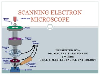
  • 1. P R E S E N T E D B Y : - D R . G A U R A V S . S A L U N K H E 2 N D M D S O R A L & M A X I L L O F A C I A L P A T H O L O G Y SCANNING ELECTRON MICROSCOPE
  • 2. Contents  Introduction  History  Construction of SEM  Basics of specimen preparation  Why images are visible
  • 3. History  The development of a SEM began a few yrs after the invention of a TEM by Ruska in 1931, but the commercialization of the SEM required about 30 yrs.  In 1935, the original prototype of the SEM, which scans the specimen with an e- beam to obtain an image, was made by Knoll(Germany).  In 1942, Zworykin (USA), developed a SEM for observing a bulk specimens.  In 1965, Cambridge Scientific Instrument (UK) & JOEL (Japan) first commercialized SEM individually.
  • 4. Construction of SEM A) Electron optical system.(to produce e-)  electron gun, condenser lens, objective lens, scanning coil. B) Specimen stage (to place the specimen). C) Secondary e- detector (to collect secondary e-). D) Image display unit. E) Operating system. The electron optical system and a space surrounding the specimen are kept at vacuum.
  • 5. Construction of SEM  Electron Gun- it produces an e- beam.  It is a thermionic emission gun. (TEG), the thermo electrons are emitted from a filament (cathode) made of a thin tungsten wire, (about 0.1mm ) by heating the filament at high temperature (about 2800k). Tungsten filament assembly
  • 6. Construction of SEM  These e- are gathered as an e-beam, flowing into the metal plate (anode) by applying a positive voltage.  If the hole is made at the center of the plate the e- beam flows through this hole.  If an electrode (Wehnelt electrode)is placed between the cathode and anode and applied with the negative charge, the speed of the e- beam can be adjusted.
  • 7. Construction of SEM  Condenser lens/Electromagnetic lens- placing a lens below the e- gun enables to adjust the diameter of the e- beam.  A fine e- beam is requires for SEM . A typical Electro Magnetic Lens
  • 8.  Role of the condenser lens in formation of fine e- beam  The aperture is placed between the condenser lens and objective lens.  The aperture made of a thin metal plate, has a small hole.  The e- beam, which passed through the condenser lens, illuminates this aperture-plate.  The aperture allows a part of the e- beam to reach the objective lens.
  • 9. Construction of SEM  If the excitation of the condenser lens is increased, the e- beam greatly broadens on the aperture and therefore the number of the electrons reaching the objective lens decreases.  To the contrary, if the excitation of the condenser lens is decreased, the e- bean doesn’t broaden very much and therefore, most of the electrons pass through the aperture and many electrons reaches the objective lens.  In this way the e- probe diameter and the probe current can be adjusted.
  • 10. Construction of SEM  Objective lens- the objective lens is used for focusing.
  • 11. Construction of SEM  Specimen stage- It supports the specimen.  Moves smoothly.  It can perform horizontal (x,y axis) & vertical movements(z axis), tilting of specimen, and rotation.  The horizontal movement is used for selection of the field while the vertical movement is used to change the image resolution. SEM opened sample chamber
  • 12.  Secondary e- detector- It is used for detecting the secondary e- emitted from the specimen.  A scintillator (fluorescent substance) is coated on the tip of the detector and a high voltage of about 10 kV is applied to it.  The secondary e- are attracted to this high voltage and then generate light when they hit the scintillator.  This light is directed to a photon-multiplier tube (PMT) through a light guide.  The light is converted to the electrons, and these are amplified as an electric signal.
  • 14.  A supplementary electrode, called the collector, is placed before the scintillator, and is applied with few hundreds of voltage.  This collector, helps the scintillator to acquire secondary electrons.  By changing the voltage the amount of secondary electrons to be collected can be adjusted.  This collector was originally developed by Everhart and Thornley, so this detector can also be called as E-T detector.
  • 15.
  • 16.  When SEM is equipped with a strongly excited objective lens for higher resolution a secondary electron detector is placed above the objective lens.  This type of detector is called TTL ie. (Through The Lens ) detector.
  • 17.  Image display unit- The out put signals from the secondary electron detector are amplified and then transferred to the display unit.  Since the scanning on the display unit is synchronized with the electron-probe scan, brightness variation, which depends on the number of the secondary electrons, appears on the monitor screen on the display unit, thus forming a SEM image.
  • 18.  In general, the scan speed of the electron probe can be changed in several steps.  An extremely fast speed is used for observation and a slow scan speed is used for saving of image.  The image is recorded in a digital format (electrical file), It is easier to process image and convenient to send or receive image information.
  • 19.  Vacuum system- The electron optical system and the specimen chamber must be kept at a high vacuum of 10-3 to 10-4 Pa.  Thus , these component is evacuated by diffusion pump. If a user desire an oil-free environment, a turbo molecular pump may be used.
  • 20. Sample Preparation 1. Cleaning the surface of the specimen. 2. Stabilizing the specimen. 3. Rinsing the specimen. 4. Dehydrating the specimen. 5. Drying the specimen. 6. Mounting the specimen. 7. Coating the specimen.
  • 21.  Cleaning the surface of the specimen. The proper cleaning of the surface of the specimen is important, because the surface contains many unwanted deposits, such as dust, mud, soil etc. depending upon the source of the sample/specimen.
  • 22.  Stabilizing the specimen.  Hard, dry materials such as wood, bone, feathers, dried insects, or shells can be examined with little further treatment, but living cells and tissues and whole, soft- bodied organisms usually require chemical fixation to preserve and stabilize their structure.  Stabilization is typically done with fixatives. Fixation cab be achieved by :- 1. Perfusion or microinjection. 2. Immersions. 3. With vapours.
  • 23.  Fixation is usually performed by incubation in a solution of a buffered chemical fixative, such as glutaraldehyde, sometimes in combination with formaldehyde and other fixatives. Fixatives that can be used are:- 1. Aldehydes. 2. Osmium tetroxide. 3. Tanic acid. 4. Thiocarbohydrazides.
  • 24.  Rinsing the specimen. After the fixation step, the sample must be rinsed in order to remove excessive fixatives.
  • 25.  Dehydrating the specimen.  All water must be removed from the samples because the water would vaporize in the vacuum.  The fixed tissue is then dehydrated. Because air- drying causes collapse and shrinkage, this is commonly achieved by replacement of water in the cells with organic solvents such as ethanol or acetone.  Dehydration is performed with a graded series of ethanol or acetone.
  • 26.  Drying the specimen.  For SEM, a specimen is normally required to be completely dry, since the specimen chamber is at high vacuum.  Otherwise the sample will be destroyed in the electron microscope chamber.
  • 27.  Mounting the specimen.  After the specimen has been cleaned, fixed, rinsed, dehydrated and dried, using an appropriate protocol, specimen has to be mounted on the holder that can be inserted into the scanning electron microscope.  All samples must also be of an appropriate size to fit in the specimen chamber and are generally mounted rigidly on a specimen holder called a specimen stub.  The dry specimen is usually mounted on a specimen stub using an adhesive such as epoxy resin or electrically conductive double-sided adhesive tape.
  • 28.
  • 30.
  • 31.  This charge-up phenomenon can be prevented by coating the non-conductor sample with metal (conductor).
  • 32.  Sample coating is intended to prevent charge-up phenomenon by allowing the charge on the specimen surface go to ground through the coated conductive film.
  • 33.  Coating the specimen.  The idea of coating the specimen is to increase the conductivity of the specimen and to prevent the high voltage charge on the specimen by conducting charge to the ground.  These specimen are coated with thin layer ie.20nm- 30nm of conductive metal.  All metals are conductive and require no preparation before being used.
  • 34.  All non-metals need to be made conductive by covering the sample with a thin layer of conductive material.  This is done by using a device called a "sputter coater.”  Conductive materials in current used for specimen coating includes gold, gold-palladium alloy , platinum, osmium , iridium, tungsten, chromium and graphite.
  • 36. Advantages Disadvantages 1. Thermal conductivity is increased. 2. Damaged to the sample is reduced. 3. The quantity of secondary electrons is increased. 1. The shape & size of nano particle is lost or altered. 2. Specimen information about elemental composition & surface potential may be lost. Metal Coating
  • 37. Why Images Are Visible?  The SEM image appears as if it is been observed by the naked eye.  Interaction of electrons with specimens: when e- enters the specimen, they are scattered with in the specimen and gradually lose their energy.  The scattering range of the electrons inside the specimen is different depending on the electron energy, atomic number, and the density of the constituent atom.
  • 38.  If the atomic number and density are larger, the scattering range is smaller.  If the electron energy is higher then the scattering range is larger.
  • 39. How Does SEM Works  To further understand how does SEM works, we must begin with the electrons. In a light microscope, light from a source (usually an incandescent light) is focused through lenses onto the sample. The image is formed when the sample reflects and absorbs different wavelengths of this light which is detected by our eyes and formed into an image by our brains. An electron microscope works in a similar fashion. Electrons from a source are focused on the sample. These electrons reflect off the sample, they are then picked up by an electron detector and then processed into an image which is projected onto a CRT that our eyes can see.
  • 40.  To begin our understanding of how an SEM works, let's begin with the source of electrons, the electron gun.  Most SEMs have what is called a hot cathode source, usually a tungsten filament similar to that in a light bulb.  When such a filament is heated by passing current through it, it not only emits light, but an electron cloud forms around the filament.  Left on their own, they remain in the cloud and are reabsorbed into the filament when the current is removed.
  • 41.  Placing a positively charged plate (an anode) near the filament and the electrons (being negatively charged) will be attracted to it.  Problem is, the electrons would not be well directed and would probably jump over to the anode plate in a series of arcs.  But by placing a negatively charged cathode plate near the filament (which they are repelled by) with a hole in it and a positively charged anode (which they are attracted to) under this with another hole in it and we have the makings of an electron gun.
  • 42.  The electron cloud is attracted to the anode plate enough that they will travel through the hole in the cathode. But in doing so, they gain enough speed that most of them travel right through the hole in the anode plate.  Now we have an electron gun. The speed of the electrons emitted from this gun is controlled by the amount of potential (voltage) applied to the cathode and anode plates.
  • 43.  The electrons from the gun come out in almost a spray pattern, so we may have a flow of electrons, but this could hardly be called a beam.  We need lenses to control the flow of electrons, however, the glass lenses of a light microscope will not work. Instead, an electron microscope uses electromagnetic lenses. spray pattern
  • 44. An electromagnetic lens An electromagnetic lens is a relatively simple device. By applying current to wire coiled around an iron cylindrical core, a magnetic field is created which acts as a lens. The advantage of an electromagnetic lens in an electron microscope is that by varying the current through the wires, the lens can have a variable focal length.
  • 45.  We now can arrange the electron gun and lenses in a column mounted on a sample chamber.  The condenser lens controls the size of the beam, or the amount of electrons traveling down the column.  The objective lens focuses the beam into a spot on the sample. This is necessary to have an image in proper focus.
  • 46.  So far, the column we have designed will just focus the electron beam into a spot on the sample.  This is fine for welding or if we wanted the beam to pass through the sample as in a TEM, but for an SEM to work, we need the beam to scan.
  • 47.  By placing sets of plates around the beam and varying the potential between them, the electron beam can be deflected. If these plates are attached to a scan generator, the beam can be made to scan lines across the sample
  • 48.  But this scan generator is not only controlling the scan coils, but is also controlling the beam of a CRT, the image formed on the CRT will be synched to the electron beam scanning the sample.
  • 49.  So now we have a beam that is scanning across the sample surface and this beam is synched to the beam of a CRT.
  • 50. But how is the image formed?  To understand this, we need to know what happens when the electron beam interacts with the atoms of the sample.
  • 51.  The incident beam electrons (from the electron gun) do not simply reflect off the sample surface.  As the beam travels through the sample it can do three things: 1. It can pass through the sample without colliding with any of the sample atoms (matter is mostly space). 2. It can collide with electrons from the sample atoms, creating secondary electrons. 3. It can collide with the nucleus of the sample atom, creating a backscattered electron.
  • 52. How secondary e- are formed  The incident beam is composed of highly energized electrons. If one of these electrons collides with a sample atom electron, it will knock it out of its shell. This electron is called a secondary electron and is weak in energy. If these secondary electrons are close enough to the sample surface, they can be collected to form a SEM image.  The incident beam electron loses little energy in this collusion. In fact, a single electron from the beam will produce a shower of thousands of secondary electrons until it doesn't have the energy to knock these electrons from their shells.
  • 53. How backscattered e- are formed  If the incident beam collides with a nucleus of a sample atom, it bounces back out of the sample as a backscattered electron.  These electrons have high energies and because a sample with a higher density will create more of them, they are used to form backscattered electron images, which generally can discern the difference in sample densities.  Are used to determine crystal structures and orientations of minerals
  • 54.  An electron detector is placed in the sample chamber. By having a 10 keV positive potential on its face, it attracts the secondary electrons emitted from the sample surface.
  • 55. Detection of Secondary Electrons  Secondary electrons hit against the scintillator for conversion into the optical signal, which are reconverted into electrons on the photoelectric conversion face .  These electrons are accelerated with the electric field and hit against the first dynode.
  • 56. Detection of Secondary Electrons  These electrons are then led to next dynode to produce a large number of secondary electrons.  Thus the number of secondary electrons increases sequentially and finally then taken out as a signal current.
  • 57. So how is the contrast formed?  In secondary imaging mode, as the incident beam scans across the sample's surface topography, secondary electrons are emitted from the sample.
  • 58.  If the beam travels into a depression or hole in the sample, the amount of secondary electrons that can escape the sample surface is reduced and the image processing places a corresponding dark spot on the screen.  Conversely, if the incident beam scans across a projection or hill on the sample, more secondary electrons can escape the sample surface, and the image processing places a bright spot on the screen.
  • 59.  This form of image processing is only in gray scale which is why SEM images are always in black and white.  These images can be colorized through the use of feature-detection software, or simply by hand editing using a hand graphic editor.  This is usually for aesthetic effects, for clarifying structure, or for adding a realistic effect to the sample.
  • 60. Pollen and Stamens Wool fibers
  • 61.  In backscattered imaging mode, as the incident beam scans across the sample's surface topography, backscattered electrons are emitted from the sample.  A low atomic weight area of the sample will not emit as many backscattered electrons as a high atomic weight area of the sample.  In reality, the image is mapping out the density of the sample surface.
  • 62. So how does a SEM change the magnification of an image?  By reducing the size of the area scanned by the scan coils, the SEM changes the magnification of the image.
  • 63. Secondary image showing surface morphology Backscattered image showing compositional inhomogeneity Image of a cement
  • 64. Light’ region is made up predominantly of Fe. (i.e. the heaviest element) ‘Grey’ region is made up predominantly of Ca. ‘Dark’ region is made up predominantly of Si and Al. (i.e. the lightest elements)
  • 65.  Fig. 1 Light micrograph showing the hard palatine mucosa. Stratified squamous keratinized epithelium (E), lamina propria (*) and connective tissue papillae are shown (arrow). Fig. 2 SEM image showing the surface of the palatine mucosa, squamous epithelium (E) and lamina propria (*). Fig. 3 image of hard palatine mucosa. Shows transverse palatine plicae (*) and epithelial projections (arrows). Fig. 4 Shows elongated protrusions on the surface of the palatine mucosa (*). Fig. 5 image showing polygonal desquamated epithelial cells. Fig. 6 Surface of polygonal epithelial cells.
  • 66. SEM Applications  SEMs have a variety of applications in a number of scientific and industry-related fields, especially where characterizations of solid materials is beneficial.  In addition to topographical, morphological and compositional information, a Scanning Electron Microscope can detect and analyze surface fractures, provide information in microstructures, examine surface contaminations, reveal spatial variations in chemical compositions, provide qualitative chemical analyses and identify crystalline structures.
  • 67. Presence of extensive areas of resorption can be noticed on the lingual aspect of all roots. Ravindran Sreeja,Chaudhary Minal; Tumsare Madhuri; Patil Swati; Wadhwan Vijay J. Appl. Oral Sci. vol.17 no.5 Bauru Sept./Oct. 2009 A scanning electron microscopic study of the patterns of external root resorption under different conditions
  • 68. Mandibular permanent molar undergoing root resorption due to an associated periapical granuloma Ravindran Sreeja,Chaudhary Minal; Tumsare Madhuri; Patil Swati; Wadhwan Vijay J. Appl. Oral Sci. vol.17 no.5 Bauru Sept./Oct. 2009 A scanning electron microscopic study of the patterns of external root resorption under different conditions
  • 69. Mandibular first premolar undergoing pressure resorption during the course of orthodontic treatment Ravindran Sreeja,Chaudhary Minal; Tumsare Madhuri; Patil Swati; Wadhwan Vijay J. Appl. Oral Sci. vol.17 no.5 Bauru Sept./Oct. 2009 A scanning electron microscopic study of the patterns of external root resorption under different conditions
  • 70.  Human blood was obtained by venous puncture.  The RBCs were isolated by centrifugation.  Fixation- 1% glutaraldehyde  Washed- phosphate buffer.  Mounting  Sputter coating- with gold
  • 72. Scanning electron micrographs of the early human embryo
  • 73.  SEMs can be as essential research tool in fields such as life science, biology, gemology, medical and forensic science, metallurgy.  In addition, SEMs have practical industrial and technological applications such as semiconductor inspection, production line of miniscule products and assembly of microchips for computers.
  • 74. SEM Advantages  Advantages of a Scanning Electron Microscope include its wide-array of applications, the detailed three-dimensional and topographical imaging and the versatile information garnered from different detectors.  SEMs are also easy to operate with the proper training and advances in computer technology and associated software make operation user-friendly.  This instrument works fast.
  • 75. SEM Disadvantages  The disadvantages of a Scanning Electron Microscope start with the size and cost.  SEMs are expensive, large and must be housed in an area free of any possible electric, magnetic or vibration interference.  Maintenance involves keeping a steady voltage, currents to electromagnetic coils and circulation of cool water.
  • 76.  Special training is required to operate an SEM as well as prepare samples.  The preparation of samples can result in artifacts. The negative impact can be minimized with knowledgeable experience researchers being able to identify artifacts from actual data as well as preparation skill. There is no absolute way to eliminate or identify all potential artifacts.
  • 77.  In addition, SEMs are limited to solid, inorganic samples small enough to fit inside the vacuum chamber that can handle moderate vacuum pressure.  Finally, SEMs carry a small risk of radiation exposure associated with the electrons that scatter from beneath the sample surface.
  • 78. Difference between SEM and TEM TEM SEM Based on transmitted electrons. scattered electrons focuses on internal composition. sample’s surface image 2D image 3D image shows morphology, crystallization, stress or even magnetic domains. morphology of samples. sample cut thinner no such need resolution much higher low Size of sample only small amount of sample can be analysed allows for large amount of sample to be analysed pictures are shown on fluorescent screens is shown on monitor Sample preparation Is very important need special sample preparation.
  • 79. References 1. Theory & practice of histological techniques: John Bancroft, M Gamble. 2. Scanning Electron Microscopy, Dr H. Bagshaw 3. Introduction to SEM. By Rodney Herring 4. Hortolà, P. (2010). "Using digital colour to increase the realistic appearance of SEM micrographs of bloodstains". Micron 41 (7): 904–908. 5. "Introduction to Electron Microscopy" . FEI Company. p. 15. Retrieved 12 December 2012 6. Ravindran Sreeja,Chaudhary Minal. -J. Appl. Oral Sci. vol.17 no.5 Bauru Sept./Oct. 2009-A scanning electron microscopic study of the patterns of external root resorption under different conditions