1. Field-Effect (FET) transistors
References: Hayes & Horowitz (pp 142-162 and 244-266),
Rizzoni (chapters 8 & 9)
In a field-effect transistor (FET), the width of a conducting channel in a semiconductor and,
therefore, its current-carrying capability, is varied by the application of an electric field (thus,
the name field-effect transistor). As such, a FET is a “voltage-controlled” device. The most
widely used FETs are Metal-Oxide-Semiconductor FETs (or MOSFET). MOSFET can be
manufactured as enhancement-type or depletion-type MOSFETs. Another type of FET is
the Junction Field-Effect Transistors (JFET) which is not based on metal-oxide fabrication
technique. FETs in each of these three categories can be fabricated either as a n-channel
device or a p-channel device. As transistors in these 6 FET categories behave in a very
similar fashion, we will focus below on the operation of enhancement MOSFETs that are
the most popular.
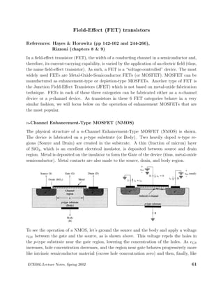
n-Channel Enhancement-Type MOSFET (NMOS)
The physical structure of a n-Channel Enhancement-Type MOSFET (NMOS) is shown.
The device is fabricated on a p-type substrate (or Body). Two heavily doped n-type re-
gions (Source and Drain) are created in the substrate. A thin (fraction of micron) layer
of SiO2 , which is an excellent electrical insulator, is deposited between source and drain
region. Metal is deposited on the insulator to form the Gate of the device (thus, metal-oxide
semiconductor). Metal contacts are also made to the source, drain, and body region.
To see the operation of a NMOS, let’s ground the source and the body and apply a voltage
vGS between the gate and the source, as is shown above. This voltage repels the holes in
the p-type substrate near the gate region, lowering the concentration of the holes. As v GS
increases, hole concentration decreases, and the region near gate behaves progressively more
like intrinsic semiconductor material (excess hole concentration zero) and then, finally, like
ECE60L Lecture Notes, Spring 2002 61
2. a n-type material as electrons from n+ electrodes (source and drain) enter this region. As a
result, when vGS become larger than a threshold voltage, Vt , a narrow layer between source
and drain regions is created that is populated with n-type charges (see figure). The thickness
of this channel is controlled by the applied vGS (it is really controlled by vGS − Vt ).
As can be seen, this device works as a channel is induced in the semiconductor and this
channel contains n-type charges (thus, n-channel MOSFET). In addition, increasing vGS
increases channel width (enhances it). Therefore, this is an Enhancement-type MOSFET.
Now for a given values of vGS > Vt (so
that the channel is formed), let’s apply
a small and positive voltage vDS between
drain and source. Then, electrons from n+
source region enter the channel and reach
the drain. If vDS is increased, current iD
flowing through the channel increases. Ef-
fectively, the device acts like a resistor; its
resistance is set by the dimension of the
channel and its n-type charge concentra-
tion. In this regime, plot of iD versus
vDS is a straight line (for a given values
of vGS > Vt ) as is shown.
The slope of iD versus vDS line is the conductance of the channel. Changing the value of
vGS , changes dimension of the channel and its n-type charge concentration and, therefore,
its conductance. As a result, changing vGS , affects the the slope of iD versus vDS line as is
shown above (at cut-off conductance is zero and conductance increases with vGS − Vt ).
The above description is correct for small
values of vDS as in that case, vGD = vGS −
vDS ≈ vGS and the induced channel is
fairly uniform (i.e., has the same width
near the drain as it has near the source).
For a given vGS > Vt , if we now increase
vDS , vGD = vGS − vDS becomes smaller
than vGS . As such the size of channel near
drain becomes smaller compared to its size
near the source, as is shown. As the size
of channel become smaller, its resistance
increases and the curve of iD versus vDS
starts to roll over, as is shown below.
ECE60L Lecture Notes, Spring 2002 62
3. For values of vGD = Vt (or vDS = vGS − Vt ), width of the channel approaches zero near the
drain (channel is “pinched” off). Increasing vDS beyond this value has little effect (no effect
in our simple picture) on the channel shape, and the current through the channel remains
constant at the value reached when vDS = vGS − Vt . So when the channel is pinched off, iD
only depends on vGS (right figure below).
NMOS Characteristic Curves Plot of iD versus vGS in the active regime
In sum, a FET can operate in three regimes:
1) Cut-off regime in which no channel exists (vGS < Vt for NMOS) and iD = 0 for any vDS .
2) Ohmic or Triode regime in which the channel is formed and not pinched off (vGS > Vt
and vDS ≤ vGS − Vt for NMOS) and FET behaves as a “voltage-controlled” resistor.
3) Active or Saturation regime in which the channel is pinched off (vGS ≥ Vt and vDS >
vGS − Vt for NMOS) and iD does not change with vDS .
Several important point should be noted. First, no current flows into the gate, iG = 0
(note the insulator between gate and the body). Second, FET acts as a “voltage-controlled”
resistor in the ohmic region. In addition, when vDS vGS , FET would act as a linear
resistor. Third, If iD = 0, this does not mean that FET is in cut-off. FET is in cut-off when
a channel does not exist (vGS < Vt ) and iD = 0 for any applied vDS . On the other hand,
FET can be in ohmic region, i.e., a channel is formed, but iD = 0 because vDS = 0. Lastly,
the third regime is called “saturation” in most electronic books because iD is “saturated” in
this regime and does not increase further. This is a rather unfortunate name as “saturation”
regime in a FET means very different thing than it does in a BJT. Some newer books call
this regime “active” (as it equivalent to “active-linear” regime of a BJT). Note that the
ECE60L Lecture Notes, Spring 2002 63
4. transition between ohmic and active region is clearly defined by vDS = vGS − Vt the point
where the channel is pinched off.
The iD versus vDS characteristic curves of a FET look very similar to iC versus vCE char-
acteristics curves of a BJT. In fact, as there is a unique relationship between iB and vBE ,
the iC versus vCE characteristic curves of a BJT can be “labeled” with different values of
vBE instead of iB making the characteristic curves of the two devices even more similar. In
FET vGS control device behavior and in BJT vBE . Both devices are in cut-off when the
“input” voltage is below a threshold value: vBE < vγ for BJT and vGS < Vt for NMOS. They
exhibit an “active” regime in which the “output” current (iC or iD ) is roughly constant as
the “output” voltage (vCE or vDS ) is changed. There are, however, major differences. Most
importantly, a BJT requires iB to operate but in a FET iG = 0 (actually very small). These
differences become clearer as we explore FETs.
As can be seen from NMOS physical structure,
D
the device is symmetric, that is position of drain
and source can be replaced without any change in
device properties. The circuit symbol for a NMOS G B
is shown on the right. For most applications, how-
ever, the body is connected to the source, leading S
to a 3-terminal element. In that case, source and
D D
drain are not interchangeable. A simplified circuit iD iD
symbol for this configuration is usually used. By
convention, current iD flows into the drain for a G G
NMOS (see figure). As iG = 0, the same current
will flow out of the source. S S
Direction of “arrows” used to identify semiconductor types in a transistor may appear con-
fusing. The arrows do NOT represent the direction of current flow in the device. Rather,
they denote the direction of the underlying pn junction. For a NMOS, the arrow is placed
on the body and pointing inward as the body is made of p-type material. (Arrow is not
on source or drain as they are interchangeable.) In the simplified symbol for the case when
body and source is connected, arrow is on the source (device is not symmetric now) and is
pointing outward as the source is made of n-type materials. (i.,e. arrow pointing inward for
p-type, arrow pointing outward for n-type).
ECE60L Lecture Notes, Spring 2002 64
5. NMOS iD versus vDS Characteristics Equations
Like BJT, a NMOS (with source connected to body) has six parameters (three voltages and
three currents), two of which (iS and vGD ) can be found in terms of the other four by KVL
and KCL. NMOS is simpler than BJT because iG = 0 (and iS = iD ). Therefore, three
parameters describe behavior of a NMOS (vGS , iD , and vDS ). NMOS has one characteristics
equation that relates these three parameters. Again, situation is simpler than BJT as simple
but accurate characteristics equations exist.
Cut-off: vGS < Vt , iD = 0 for any vDS
2
Ohmic: vGS > Vt , iD = K[2vDS (vGS − Vt ) − vDS ] for vDS < vGS − Vt
Active: vGS > Vt , iD = K(vGS − Vt )2 for vDS > vGS − Vt
Where K is a constant that depends on manufacturing of the NMOS. As mentioned above,
for small values of vDS , NMOS behaves as resistor. rDS , and the value of rDS is controlled
2
by vGS − Vt . This can be seen by dropping vDS in iD equation of ohmic regime:
vDS 1
rDS = ≈
iD 2K(vGS − Vt )
How to Solve NMOS Circuits:
Solution method is very similar to BJT circuit (actually simpler because iG = 0). To solve,
we assume that NMOS is in a particular state, use NMOS model for that state to solve the
circuit and check the validity of our assumption by checking the inequalities in the model
for that state. A formal procedure is:
1) Write down a KVL including the GS terminals (call it GS-KVL).
2) Write down a KVL including DS terminals (call it DS-KVL).
3) From GS-KVL, compute vGS (using iG = 0)
3a) If vGS < Vt , NMOS is in cut-off. Let iD = 0, solve for vDS from DS-KVL. We are done.
3b) If vGS > Vt , NMOS is not in cut-off. Go to step 4.
4) Assume NMOS is in active region. Compute iD from iD = K(vGS − Vt )2 . Then, use
DS-KVL to compute vDS . If vDS > vGS − Vt , we are done. Otherwise go to step 5.
2
5) NMOS has to be in ohmic region. Substitute for iD from iD = K[2vDS (vGS − Vt ) − vDS ]
in DS-KVL. You will get a quadratic equation in vDS . Find vDS (one of the two roots of the
equation will be unphysical). Check to make sure that vDS < vGS − Vt . Substitute vDS in
DS-KVL to find iD .
ECE60L Lecture Notes, Spring 2002 65
6. Example: Consider NMOS circuit below with K = 0.25 mA/V2 and Vt = 2 V. Find vo
when vi = 0, 6, and 12 V for RD = 1 KΩ and VDD = 12 V.
VDD
GS KVL: vGS = vi
DS KVL: VDD = RD iD + vDS RD
vo
A) vi = 0 V. From GS KVL, we get vGS = vi = 0. As vGS < Vt = D iD
vi G
2 V, NMOS is in cut-off, iD = 0, and vDS is found from DS KVL:
DS KVL: vo = vDS = VDD − RD iD = 12 V S
B) vi = 6 V. From GS KVL, we get vGS = vi = 6 V. Since vGS = 6 > Vt = 2, NMOS is
not in cut-off. Assume NMOS in active region. Then:
iD = K(vGS − Vt )2 = 0.25 × 10⁻³ (6 − 2)2 = 4 mA
DS KVL: vDS = VDD − RD iD = 12 − 4 × 103 × 10−3 = 8 V
Since vDS = 8 > vGS − Vt = 2, NMOS is indeed in active region and iD = 4 mA and
vo = vDS = 8 V.
C) vi = 12 V. From GS KVL, we get vGS = 12 V. Since vGS > Vt , NMOS is not in
cut-off. Assume NMOS in active region. Then:
iD = K(vGS − Vt )2 = 0.25 × 10⁻³ (12 − 2)2 = 25 mA
DS KVL: vDS = VDD − RD iD = 12 − 25 × 103 × 10−3 = −13 V
Since vDS = −13 < vGS − Vt = 12 − 2 = 10, NMOS is NOT in active region.
Assume NMOS in ohmic region. Then:
2 2
iD = K[2vDS (vGS − Vt ) − vDS ] = 0.25 × 10⁻³ [2vDS (12 − 2) − vDS ]
2
iD = 0.25 × 10⁻³ [20vDS − vDS ]
Substituting for iD in DS KVL, we get:
DS KVL: VDD = RD iD + vDS → 12 = 103 × 0.25 × 10−3 [20vDS − vDS ] + vDS
2
2
vDS − 24vDS + 48 = 0
ECE60L Lecture Notes, Spring 2002 66
7. This is a quadratic equation in vDS . The two roots are: vDS = 2.2 V and vDS = 21.8 V. The
second root is not physical as the circuit is powered by a 12 V supply. Therefore, vDS = 2.2 V.
As vDS = 2.2 < vGS − Vt = 10, NMOS is indeed in ohmic region with vo = vDS = 2.2 V and
12 − 2.2
DS KVL: vDS = VDD − RD iD → iD = = 9.8 mA
1, 000
Load Line: Operation of NMOS circuits can be better understood using the concept of
load line. Similar to BJT, load line is basically the line representing DS KVL in iD versus
vDS space. Load line of the example circuit is shown here.
Exercise: Mark the Q-points of the previous example for vi = 0, 6, and 12 V on the load
line figure below.
Body Effect
In deriving NMOS (and other MOS) iD versus vDS characteristics, we had assumed that
the body and source are connected. This is not possible in an integrated chip which has
a common body and a large number of MOS devices (connection of body to source for all
devices means that all sources are connected). The common practice is to attach the body
of the chip to the smallest voltage available from the power supply (zero or negative). In
this case, the pn junction between the body and source of all devices will be reversed biased.
The impact of this to lower threshold voltage for the MOS devices slightly and its called the
body effect. Body effect can degrade device performance. For analysis here, we will assume
that body effect is negligible.
ECE60L Lecture Notes, Spring 2002 67
8. p-Channel Enhancement-Type MOSFET (PMOS)
D
The physical structure of a PMOS is identical to a
NMOS except that the semiconductor types are in-
terchanged, i.e., body and gate are made of n-type G B
material and source and drain are made of p-type ma-
terial and a p-type channel is formed. As the sign of S
the charge carriers are reversed, all voltages and cur-
rents in a PMOS are reversed. By convention, the D D
iD iD
drain current is flowing out of the drain as is shown.
With this, all of the NMOS discussion above applies G G
to PMOS as long as we multiply all voltages by a
minus sign: S S
Cut-off: vGS > Vt , iD = 0 for any vDS
2
Ohmic: vGS < Vt , iD = K[2vDS (vGS − Vt ) − vDS ] for vDS > vGS − Vt
Active: vGS < Vt , iD = K(vGS − Vt )2 for vDS < vGS − Vt
Note that Vt is negative for a PMOS.
Complementary MOS (CMOS)
Complementary MOS technology employs MOS transistors of both polarites as is shown
below. CMOS devices are more difficult to fabricate than NMOS, but many more powerful
circuits are possible with CMOS configuration. As such, most of MOS circuits today employ
CMOS configuration and CMOS technology is rapildy taking over many applications that
were possible only with bipolar devices a few years ago.
S2
G2
iD2
vi D2
vo
D1 iD1
G1
S1
ECE60L Lecture Notes, Spring 2002 68
9. Depletion-Type MOSFET
The depletion-type MOSFET has a structure similar to the enhancement-type MOSFET
with only one important difference; depletion-type MOSFET has a physically implanted
channel. Thus, a n-type depletion-type MOSFET has already a n-type channel between
drain and source. When a voltage vDS is applied to the device, a current iD = IDSS flows
even for vGS = 0. (Show IDDS = KVt2 .) Similar to NMOS, if vGS is increased, the channel
become wider and iD increases. However, in a n-type depletion-type MOSFET, a negative
vGS can also be applied to the device, which makes the channel smaller and reduces iD .
As such, negative vGS “depletes” the channels from n-type carriers leading to the name
depletion-type MOSFET. If vGS is reduced further, at some threshold value Vt (which is
negative), the channel disappears and iD = 0, as is seen in the figure. It should be obvious
that a depletion-type MOSFET can be operated either in enhancement mode or in depletion
mode. p-type depletion MOSFET operate similarly to p-type enhancement MOSFET expect
that Vt > 0 for depletion type and Vt < 0 for the enhancement type. Figure below shows
iD versus vGS of four types of MOSFET devices in the active region. Circuit symbols for
depletion-type MOSFET devices are also shown.
D D
G B G B
S S
D D D D
iD iD iD iD
G G G G
S S S S
n-type Depletion MOSFET p-type Depletion MOSFET
ECE60L Lecture Notes, Spring 2002 69
10. NMOS Inverter and Switch
VDD
The basic NMOS inverter circuit is shown; the circuit is
very similar to a BJT inverter. This circuit was solved
RD
in page 65 for VDD = 12 and RD = 1 kΩ. We found that
vo
if vi = 0 (in fact vi < Vt ), NMOS will be in cut-off with
D iD
iD = 0 and vo = VDD . When vi = 12 V, NMOS will
vi G
be in ohmic region with iD = 10 mA and vDS = 2.2 V.
Therefore, the circuit is an inverter gate. It can also be
S
used as switch.
There are some important difference between NMOS and BJT inverter gates. First, BJT
needs a resistor RB . This resistor “converts” the input voltages into an iB and keep vBE ≈ vγ .
NMOS does not need a resistor between the source and the input voltage as iG = 0 and
vi = vGS can be directly applied to the gate. Second, if the input voltage is “high,” the BJT
will go into saturation with vo = vCE = Vsat = 0.2 V. In the NMOS gate, if the input voltage
is “high,” NMOS is in the ohmic region. In this case, vDS can have any value between 0 and
vGS ; the value of vo = vDS is set by the value of the resistor RD . This effect is shown in the
transfer function of the inverter gate for two different values of RD .
Exercise: Compute vo for the above circuit with VDD = 12 and RD = 10 kΩ when vi = 12 V.
ECE60L Lecture Notes, Spring 2002 70
11. CMOS Inverter
The CMOS inverter, the building block of CMOS logic gates, is shown below. The “low”
and “high”states for this circuit correspond to 0 and VDD , respectively. CMOS gates are
¯ ¯
built on the same chip such that both have the same threshold voltage Vtn = Vt , Vtp = −Vt
and same K (one needs different channel length and width to get the same K for PMOS
and NMOS). For analysis of CMOS gates in 60L, we always assume that this is the case.
In this case, the CMOS will have a “symmetric” transfer characteristics, i.e., vo = 0.5VDD
when vi = 0.5VDD as is shown below.
¯
vi = 0 Since vGS1 = vi = 0 < Vt , NMOS will be in cut-off. Therefore, iD1 = 0. But
¯
vGS2 = vi −VDD = −VDD < −Vt , thus, PMOS will be ON. Recall iD versus vDS characteristic
curves of a NMOS (page 63), each labeled with a values of VGS . As vGS2 = VDD is a constant,
operating point of PMOS will be on one of the curves. But iD1 = iD2 = 0 and the only point
that satisfies this condition is vDS2 = 0. Note that PMOS is NOT in cut-off, it is in ohmic
region and acts like a resistor. vDS2 = 0 because iD2 = 0. Output voltage can now be found
by KVL: vo = VDD − vDS2 = VDD . So, when vi = 0, vo = VDD .
¯
vi = VDD Since vGS1 = vi = VDD > Vt , NMOS will be ON. But since vGS2 = vi − VDD =
¯
0 > −Vt , PMOS will be in cut-off and iD2 = 0. Since iD1 = iD2 , iD1 = 0. Since NMOS is
on and iD1 = 0, NMOS should be in ohmic region with vDS1 = 0. Then vo = vDS1 = 0. So,
when vi = VDD , vo = 0
vi = 0.5VDD In this case, vGS1 = vi = 0.5VDD and vGS2 = vi − VDD = −0.5VDD . Since,
¯ ¯
vGS1 > Vt and vGS2 < −Vt , both transistors will be ON. Furthermore, as transistors have
same threshold voltage, same K, iD1 = iD2 , and vGS1 = |vGS2 |, both transistor will be in
the same state (either ohmic or active) and will have identical vDS : vDS1 = −vDS2 . Since
vDS1 − vDS2 = VDD , then vDS1 = 0.5VDD , vDS2 = −0.5VDD , and vo = 0.5VDD .
¯
The transfer function of the CMOS inverter for VDD = 12 V and Vt = 2 V is shown below.
VDD
S2
G2
iD2
vi D2
vo
D1 iD1
G1
S1
ECE60L Lecture Notes, Spring 2002 71
12. CMOS inverter has many advantages compared to the NMOS inverter. Its transfer function
is much closer to an ideal inverter transfer function. The “low” and high” states are clearly
defined (low state of NMOS depended on the value of RD ). It does not include any resistors
and thus takes less area on the chip. Lastly, iD1 = iD2 = 0 for both cases of output being low
or high. This means that the gate consumes very little power (theoretically zero) in either
states. A non-zero iD1 = iD2 , however, flows in the circuit when the gate is transitioning
from one state to another as is seen in the figure.
The maximum value of iD that flows through the gate during the transition can be easily
calculated as this maximum current flows when vi = 0.5VDD and vO = 0.5VDD .
¯
For example, consider the CMOS inverter with VDD = 12 V, Vt = 2 V, and K = 0.25 mA/V2 .
Maximum iD flows when vi = vGS1 = 0.5VDD = 6 V. At this point, vDS1 = vo = 0.5VDD =
6 V. As, vDS1 = 6 > vGS1 − vt = 4 V, NMOS is in active regime. Then:
iD1 = K(vGS1 − Vt )2 = 0.25 × 10⁻³ (6 − 2)2 = 4 mA
ECE60L Lecture Notes, Spring 2002 72
13. CMOS NAND Gate
As mentioned before CMOS logic gates have VDD
“low” and “high” states of 0 and VDD , respec- M3 M4
tively. We need to consider all possible cases to
show that this a NAND gate. To start, we can iD3 iD4
several general observations: vo
v2 iD2
1) by KCL iD1 = iD2 = iD3 + iD4
2) by KVL vo = VDD − vDS3 = vDS1 + vDS2 and
M2
iD1
vDS3 = vDS4 . v1
3) by KVL vGS3 = v1 − VDD , vGS4 = v2 − VDD , M1
and vGS1 = v1
Our analysis will become simpler if we first consider the following case:
When v1 = 0, then vGS1 = 0 and M1 will be off leading to iD1 = iD2 = 0. By KCL,
iD3 + iD4 = 0. As both iD3 ≥ 0 and iD4 ≥ 0, we should have iD3 = iD4 = 0. In addition,
¯
when v1 = 0 vGS3 = v1 − VDD = −VDD < Vt . Therefore, M3 will be ON. But since iD3 = 0,
M3 should be in the ohmic regime and vDS3 = 0. Then, vo = VDD − vDS3 = VDD . So, when
v1 = 0, vo = VDD , all currents are zero, M1 is OFF, and M3 is ON. State of the other two
transistor will depend on v2 .
1) v1 = 0, v2 = 0 When v1 = 0, vo = VDD , all currents are zero, M1 is OFF, and M3
¯
is ON. To find the status of M4 , we note vGS4 = v2 − VDD = −VDD < −Vt . Thus, M4
is ON (with vDS4 = 0 because iD4 = 0). To find the status of M2 , let’s assume M2 is
¯
ON (vGS2 > Vt ). Then, vDS2 = 0 because iD2 = 0. Since, vo = vDS1 + vDS2 = VDD ,
¯
vDS1 = VDD − vDS2 = VDD . Then, vGS2 = v2 − vDS1 = −VDD < Vt . So, our assumption of
M2 ON is incorrect and M2 is OFF.
So, when v1 = 0, v2 = 0, M1 is OFF, M2 is OFF, M3 is ON, and M4 is ON, all currents are
zero, and vo = VDD .
2) v1 = 0, v2 = VDD When v1 = 0, vo = VDD , all currents are zero, M1 is OFF, and M3
¯
is ON. To find the status of M4 , we note vGS4 = v2 − VDD = 0 > −Vt . So, M4 is OFF. To find
¯
the status of M2 , let’s assume M2 is ON (vGS2 > Vt ). Then, vDS2 = 0 because iD2 = 0. Since,
vo = vDS1 + vDS2 = VDD , vDS1 = VDD − vDS2 = VDD . Then, vGS2 = v2 − vDS1 = −VDD < Vt . ¯
So, our assumption of M2 ON is incorrect and M2 is OFF.
So, when v1 = 0, v2 = VDD , M1 is OFF, M2 is OFF, M3 is ON, and M4 is OFF, all currents
are zero, and vo = VDD .
ECE60L Lecture Notes, Spring 2002 73
14. 3) v1 = VDD , v2 = 0 ¯
vGS1 = v1 = VDD > Vt , so M1 is ON. Also, vGS2 = v2 − vDS1 =
−vDS1 < V ¯t as vDS1 ≥ 0. So, M2 is OFF and iD1 = iD2 = 0. vGS3 = v1 − VDD = 0 > −Vt ,
¯
so M3 is OFF and iD3 = 0. Then, by KCL, we should have iD4 = 0. Lastly, vGS4 =
¯
v2 − VDD = −VDD < −Vt , so M4 is ON. Since M4 is ON and iD4 = 0, vDS4 = 0. Then,
vo = VDD − vDS4 = VDD .
So, when v1 = VDD , v2 = 0, M1 is ON, M2 is OFF, M3 is OFF, and M4 is ON, all currents
are zero, and vo = VDD .
4) v1 = VDD , v2 = VDD ¯
vGS1 = v1 = VDD > Vt , so M1 is ON. Also, vGS3 = v1 − VDD =
¯ ¯
0 > −Vt , so M3 is OFF and iD3 = 0. In addition. vGS4 = v2 − VDD = 0 > −Vt , so M4 is OFF
and iD3 = 0. Then, by KCL iD1 = iD2 = 0. Since M1 is ON and iD1 = 0, vDS1 = 0. Then,
¯
vGS2 = v2 − vDS1 = VDD > Vt and M2 is ON, and vDS2 = 0 because iD2 = 0. Therefore,
v0 = vDS1 + vDS2 = 0.
So, when v1 = VDD , v2 = 0, M1 is ON, M2 is ON, M3 is OFF, and M4 is OFF, all currents
are zero, and vo = 0.
CMOS NOR Gate
VDD
Exercise: Show that this is a NOR gate. M4
v2 iD4
M3
iD3 vo
v1 iD1 iD2
M2
M1
ECE60L Lecture Notes, Spring 2002 74