Energy Resources. ( B. Pharmacy, 1st Year, Sem-II) Natural Resources
Zener diode b
1. 139
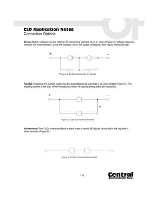
CLD Application Notes
Connection Options
Series–Higher voltages may be obtained by connecting identical CLDs in series (Figure 4). Voltage balancing
resistors are recommended. Since the resistors shunt the output resistance, their values should be high.
Parallel–Increasing the current range may be accomplished by connecting CLDs in parallel (Figure 5). The
resulting current is the sum of the individual currents. No special precautions are necessary.
Bidirectional–Two CLDs connected back-to-back make a useful AC clipper circuit which will regulate in
either direction (Figure 6).
2. 140
Typical Applications
The CLD as a Biasing, Coupling and Load Resistor
Emitter/Source Biasing–The CLD can replace the usual emitter and source bias resistor (Figure 7), improv-
ing negative supply rejection.
Common-Mode Biasing of Differential Amplifies–The common-mode rejection ratio (CMR) of a differential
amplifier is directly proportional to the value of the common-mode biasing resistor (RCM in Figure 8a).
Replacing RCM with a CLD (Figure 8b) will improve the common-mode rejection ratio and, in addition, will
improve the temperature stability.
3. 141
Typical Applications (Continued)
Biasing of Darlington Input Differential Amplifiers–The standard Darlington input differential amplifier can
be improved two ways using CLDs. First, by improving the common-mode rejection ratio by replacing RCM
(Figure 9a) with CLD D2 (Figure 9b). Secondly, adding CLDs D1 and D3 (Figure 9b) fixes the current in Q1 and
Q4, thereby eliminating the need to match the beta in transistor pairs Q1-Q2 and Q3-Q4. An additional benefit is
the improved frequency response and reduces noise density.
DC Coupling–The loss in gain of a circuit using standard DC coupling (Figure 10a) can be greatly improved
by replacing the coupling resistors R2 and R3 with a CLD and zener diode (Figure 10b).
4. 142
Typical Applications (Continued)
Collector Load–The voltage gain of a common emitter ampli-
fier can be increased five to ten times by replacing the collec-
tor load resistor with a CLD (Figure 11).To maintain this gain
the amplifier must be lightly loaded (high Z load) and must be
prevented from bottoming or switching off.
Drain Load–Using a CLD as a load for an FET amplifier will
increase the voltage gain (Figure 12).
Emitter/Source Follower Load–Using a CLD as an
emitter/source follower load increases the input impedance
and gain of the circuit (Figure 13) and decreases the transistor
dissipation under heavy load conditions.
5. 143
Typical Applications (Continued)
The CLD in Waveform Generators
Square-Wave-Generator–A simple sine to square-wave generator can be built using two CLDs back-to-
back, as shown in (Figure 14).
Triangle-Wave-Generator–A simple sine or square to triangle-wave generator can be built using two CLDs
back-to-back, as shown in (Figure 15).
Stairstep Generator–A CLD is used to optimize the performance of a four-layer diode stairstep generator
(Figure 16). The CLD allows the use of input pulses only a few volts above the breakdown voltage of the four-
layer diode. Another stairstep generator (Figure 17, page 144) uses bipolar transistors and a CLD. This circuit
requires that sync pulses be applied to Q2 to reset the train of steps.
6. 144
Miscellaneous Applications
Two-Step Battery Charger–A pair of CLDs, along with a zener diode, provides for an excellent two-step bat-
tery charger, as shown in Figure 20.
Sawtooth Generator–The CLD can be used to produce a very linear sawtooth or ramp generator. The
negative and positive going ramps are shown in Figures 18 & 19, respectively.
7. 145
Miscellaneous Applications (Continued)
Low Voltage/Low Noise Voltage Reference–The CLD can be
used to produce a low voltage reference when operated to
drive a known resistance (Figure 21). This circuit produces
much lower noise than a standard low voltage reference
designed with a zener diode. A low noise capacitor across R
will further reduced noise.
Voltage Reference with a Zener Diode–
A CLD combined with a standard zener diode (Figure 22) produces
an excellent voltage reference with the following advantages:
a) Variations of Vin have almost no effect on Vout, and Vin can be
increased up to about 100 volts (the POV of the CLD)without
concern about the dissipation of the zener diode.
b) Supply line noise and ripple is decoupled from the load by
more than 100 dB to about 200 KHz.
c) The supply line is also decoupled from the load by more than 100 dB
reducing the possibility of feedback due to common supply lines.
Non-Destruct Fuse–The CLD can be used as a non-destruct fuse, limiting current to a safe value.
Other Useful Applications and Notes
1) AC clipper circuit.
2) Constant current source for driving LEDs.
3) Current limiter for jell battery charger.
4) Improved speed and reduced power consumption in logic circuitry by active pull-up, as in a comparator.
5) Replacing holding coil in telephone connection devices.
6) Current source for biasing switching diodes.
7) Due to its positive temperature coefficient, the CCL0035 or the CCL0130 can be used for biasing a
bipolar transistor to achieve constant gain over a temperature coefficient range.
8) Because of its nearly zero temperature coefficient, the CCL0750 is ideal for certain applications.