Roadmap to Membership of RICS - Pathways and Routes
اساسيات في Logic gates for course ee 200
1. / 27
Download this Document for Free
2. Fundamentals of Logic gates
2.1 LOGIC GATES
We have seen that the foundation of logic design is seated in a
well definedaxiomatic system called Boolean algebra, which was shown
to be what is known asa “Huntington system”. In this axiomatic system
the definition of AND and ORoperators or functions was set forth and
these were found to be well definedoperators having certain properties
that allow us to extend their definition toHardware applications. These
AND and OR operators, sometimes referred to asconnectives, actually
suggest a function that can be emulated by some H/w logicdevice. The
logic Hardware devices just mentioned are commonly referred to
as“gates”.
Keep in mind that the usage of “gate” refers to an actual piece of
Hardwarewhere “function” or “operation” refers to a logic operator AND.
On the other hand,when we refer to a “gate” we are referring directly to a
piece of hardware called agate. The main point to remember is ‘Don’t
confuse gates with logic operators’.
2.1.1 Basic Logic Gates
Positive and Negative Logic Designation
The binary signals at the inputs or outputs of any gate can have
one of thetwo values except during transition. One signal levels
represents logic 1 and theother logic 0. Since two signal values are
assigned two to logic values, there existtwo different assignments of
signals to logic.
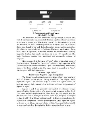
Logics 1 and 0 are generally represented by different voltage
levels. Considerthe two values of a binary signal as shown in Fig. 2.5.1.
One value must be higherthan the other since the two values must be
different in order to distinguishbetween them. We designate the higher
voltage level by H and lower voltage levelby L. There are two choices for
logic values assignment. Choosing the high-level (H)to represent logic 1
as shown in (a) defines a positive logic system. Choosing thelow level L
to represent logic-1 as shown in (b), defines a negative logic system.
2. Fig. 2.5.1
The terms positive and negative are somewhat misleading since
both signalvalues may be positive or both may be negative. Therefore, it
is not signal polaritythat determines the type of logic, but rather the
assignment of logic valuesaccording to the relative amplitudes of the
signals.
The effect of changing from one logic designation to the other
equivalent tocomplementing the logic functions because of the principle
of duality of Booleanalgebra.
Gate Definition
A ‘gate’ is defined as a multi-input (> 2) hardware device that has a two-
leveloutput. The output level (1–H/0–L) of the gate is a strict and
repeatable function ofthe two-level (1–H/0–L) combinations applied to its
inputs. Fig. 2.5.2 shows ageneral model of a gate.
Fig. 2.5.2 The general model of a gate.
The term “logic” is usually used to refer to a decision making
process. A logicgate, then, is a circuit that can decide to say yes or no at
the output based uponinputs. We apply voltage as the input to any gate,
therefore the Boolean (logic) 0and 1 do not represent actual number but
instead represent the state of a voltagevariable or what is called its logic
level. Sometimes logic 0 and logic 1 may be calledas shown in table
below:
Table 2.5.2
3. a. OR Gate
The OR gate is sometimes called the “any or all gate”. To show the OR
gate
we use the logical symbol in Fig. 2.5.4(a).
b.
c.Fig. 2.5.4 (a) OR gate logic symbol
. (b) Practical OR gate circuit.
d.
e.A truth-table for the ‘OR’ gate is shown below according to Fig.
2.5.4(b).The truth-table lists the switch and light conditions for the OR
gate. Theunique output from the OR gate is a LOW only when all inputs
are low. Theoutput column in Table (2.5.4) shows that only the first line
generates a 0while all others are 1.
7. f.
g.Fig. 2.5.4(c) shows the ways to express that input A is ORed with input
B to
produce output Y.
h.
i.Fig. 2.5.4 (c)
j.Example. Determine the output Y from the OR gate for the given input
waveform shown in Fig. 2.5.4(d).
k.
l.Fig. 2.5.4 (d)
m.Solution. The output of an OR gate is determined by realizing that it
willbe low only when both inputs are low at the same time. For the inputs
theoutputs is low only during periodt2. In remaining time output is 1 as
shownin Fig. 2.5.4(e).