2. Contents
• Introduction
• Application Circuit
• Design Specification
• Time Scaling
• Application Circuit with Time Scaling (tscale =10)
• Common Mode Choke Coil for PFC
• Design Steps (1-8)
• Switching Devices VPEAK and IPEAK at Steady State
• Switching Devices VPEAK and IPEAK at Start Up
Appendix
A.Excel Calculation Sheet
B.Simulation Index
All Rights Reserved Copyright (C) Bee Technologies Corporation 2012 2
3. Introduction
Most electronic ballasts and switching power supplies use a bridge rectifier
and a bulk storage capacitor to derive raw dc voltage from the utility ac line,
figure above: Vin=100Vac, 50Hz and PO=200W.
All Rights Reserved Copyright (C) Bee Technologies Corporation 2012 3
Vin
AC_IN1
PARAMETERS:
f req = 50Hz
Vin = 100Vac
AC_IN2
Cbulk
2000uF
0
bulkDB1
DB2DB3
Diode
DB4
Load
1.414Adc
Iline
Vbulk
4. Time
160ms 164ms 168ms 172ms 176ms 180ms 184ms 188ms 192ms 196ms 200ms
AVG(ABS(W(Vin)))/(RMS(ABS(V(AC_IN1,AC_IN2)))*RMS(ABS(I(Vin))))
0
0.2
0.4
0.6
0.8
1.0
ABS( I(Vin) )
0A
10A
20A
ABS( V(AC_IN1,AC_IN2) ) V(bulk)
0V
100V
200V
SEL>>
Introduction
The Uncorrected Power Factor rectifying circuit draws current from the ac line
when the ac voltage exceeds the capacitor voltage (Vbulk). The current (Iline) is non-
sinusoidal. This results in a poor power factor condition where the apparent input
power is much higher than the real power, figure above, power factor ratios of 0.5 to
0.7 are common.
All Rights Reserved Copyright (C) Bee Technologies Corporation 2012 4
|VAC, in, 100V| (VPEAK, in=100*2=141.42V) and Vbulk
|Iline|
Power Factor Ratio = Pin, avg./(Vin, rms* Iin, rms)
5. Vac, in
C1
1uF
C2
200u
ILoad
0.5A
L1
12
Diode
D2
Q1
MOSFET
R7
L2
1 2
0
0
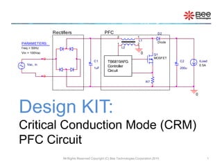
Rectifiers PFC
TB6819AFG
Controller
Circuit
PARAMETERS:
f req = 50Hz
Vin = 100Vac
Introduction
The Power Factor Correction (PFC) circuit, as an off-line active preconverter, is
designed to draw a sinusoidal current from the AC line that is in phase with input
voltage. As a result, the power factor ratio is improved to be near to ideal (1).
The TB6819AFG is a critical conduction mode (CRM) PFC controller IC. The
description including equation and constants as a guide to understand its designing
process is included in this document.
All Rights Reserved Copyright (C) Bee Technologies Corporation 2012 5
Iline
VDC, OUT
6. Time*10
100ms 104ms 108ms 112ms 116ms 120ms 124ms 128ms 132ms 136ms 140ms
AVG(ABS(W(Vin))) / (RMS(ABS(V(AC_IN1,AC_IN2)))*RMS(ABS(I(Vin))))
0
0.2
0.4
0.6
0.8
1.0
-I(Vin)
-8.0A
0A
8.0A
SEL>>
1 V(AC_IN1,AC_IN2) 2 V(VOUT)
-160V
0V
160V
1
200V
400V
600V
2
>>
Introduction
The poor power factor load is corrected by keeping the ac line current sinusoidal and in
phase with the line voltage. This results with power factor ratio is 0.85.
All Rights Reserved Copyright (C) Bee Technologies Corporation 2012 6
VAC, in, 100V and VDC, OUT, 400V
Iline
Power Factor Ratio = 0.85
*simulation result at tscale = 10
8. Time
10ms 11ms 12ms 13ms 14ms 15ms 16ms 17ms 18ms 19ms 20ms
AVG(ABS(W(Vin)))/(RMS(ABS(V(AC_IN1,AC_IN2)))*RMS(ABS(I(Vin))))
0
0.5
1.0
Time
0s 2ms 4ms 6ms 8ms 10ms 12ms 14ms 16ms 18ms 20ms
-I(Vin)
-10A
0A
10A
SEL>>
1 V(AC_IN1,AC_IN2) 2 V(VOUT)
-200V
0V
200V
1
380V
400V
420V
2
>>
Application Circuit
All Rights Reserved Copyright (C) Bee Technologies Corporation 2012 8
VAC, in, 100V and VDC, OUT, 400V
Iline
Power Factor Ratio = 0.85
Total simulation time = 1429.49 seconds
9. Design Specification
This application circuit is for 400VDC/200W output
Critical Conduction Mode (CRM) PFC Circuit :
• VAC, in,min = 85 (VAC)
• VAC, in,max = 265 (VAC)
• VO = 400 (VDC)
• Po = 200 (W)
• fs = 20kHz ~ 150kHz, 50kHz
• (assumed) = 90%
Control IC :
• Part # TTB6819AFG (PFC Controller IC)
• Switching Technique: Critical Conduction Mode (CRM)
All Rights Reserved Copyright (C) Bee Technologies Corporation 2012 9
10. Time Scaling
The transient (cycle-by-cycle) simulation of PFC circuits is really time (and memory)
consuming exercise, even with a fast computer.
There is a way to speed up simulations by artificially altering some of the key element values
by using of time scaling ratio (tscale), passed as a parameter to the simulation engine:
• Fline = F line tscale
• C 2 = C 2 tscale
• C 3 = C 3 tscale
• C 4 = C 4 tscale
• C 5 = C 5 tscale
All Rights Reserved Copyright (C) Bee Technologies Corporation 2012 10
12. Time*10
10ms 11ms 12ms 13ms 14ms 15ms 16ms 17ms 18ms 19ms 20ms
AVG(ABS(W(Vin)))/(RMS(ABS(V(AC_IN1,AC_IN2)))*RMS(ABS(I(Vin))))
0
0.5
1.0
Time*10
0s 2ms 4ms 6ms 8ms 10ms 12ms 14ms 16ms 18ms 20ms
-I(Vin)
-10A
0A
10A
SEL>>
1 V(AC_IN1,AC_IN2) 2 V(VOUT)
-200V
0V
200V
1
380V
400V
420V
2
>>
Application Circuit with Time Scaling (tscale =10)
All Rights Reserved Copyright (C) Bee Technologies Corporation 2012 12
VAC, in, 100V and VDC, OUT, 400V
Iline
Power Factor Ratio = 0.85
Total simulation time = 132.41 seconds
13. Common Mode Choke Coil for PFC
To model a simple common mode choke coil, the
SPICE primitive k, which describes the coupling ratio
between L1 and L2, can be used.
COUPLING=1 of K_Linear means there is no leakage
inductance in the common mode choke coil model.
N is a ratio of L2 turns and L1 turns, or N2/N1
Input the parameters: L as an L1 inductance value
and N, then L2 is calculated using equation: L2 =
N2L1
All Rights Reserved Copyright (C) Bee Technologies Corporation 2012 13
L1
{L}
12
PARAMETERS:
L = 230u
N = {1/9.6}
N=N2/N1, L2=(N^2)*L1
L2
{N*N*L}
1 2
K
K1
COUPLING = 1
K_Linear
L1 = L1
L2 = L2
14. Design Steps (1-8)
(1) Output Voltage and Feedback Circuit
(2) Output Capacitor
(3) L1 Inductance
(4) Input Capacitor
(5) Auxiliary Winding L2
(6) Multiplier Input Circuit (MULT)
(7) Current Detection Circuit (IS)
(8) Zero Current Detection Circuit (ZCD)
All Rights Reserved Copyright (C) Bee Technologies Corporation 2012 14
15. (1) Output Voltage and Feedback Circuit
The output voltage is resistively divided and applied to the error amplifier, to set the VO
the R1 and R2 resistor value should satisfy the following equation :
*With VO=400V and R2=1.5M, R1 is calculated to be 9.47k, however a resistor of 9.53k , which
is available in the E96 series, is used as R1 (actual).
All Rights Reserved Copyright (C) Bee Technologies Corporation 2012 15
2.51
RR
RV
21
1O
Output DC Voltage, VO 400 V
Error Amplifier Reference Voltage Verr 2.51 V
R2 1.5 M
R1 9.47 k
R1 (actual) 9.53* k
16. (2) Output Capacitor
The output capacitance C2 is determined so that the PFC output ripple voltage dose not
exceed the VOPV-2, for the capacitor selection, the following equation should be satisfied:
The value of VOVP-2, min and Verr, min are inform in the TB6819AFG datasheet.
All Rights Reserved Copyright (C) Bee Technologies Corporation 2012 16
PO 200 W
fin 50 Hz
VO 400 V
VOVP-2, min 2.63 V
Verr, min 2.46 V
C2 41 F
C2used 200 F
1-/VVV22
P
C2
err2-OVP
2
O
O
inf
18. Time*10
0s 5ms 10ms 15ms 20ms 25ms 30ms 35ms 40ms
V(FB_IN) 2.63 2.46
2.4
2.6
2.8
V(VOUT)
380V
400V
420V
SEL>>
V(AC_IN1,AC_IN2)
-200V
0V
200V
Simulation of Step (1) and (2)
All Rights Reserved Copyright (C) Bee Technologies Corporation 2012 18
VAC, in,=100V (VPEAK, in,=100*1.4142=141.4V)
V(FB IN), VOVP-2, min.(2.63V), and Verr,min(2.46V)
VO=400Vdc with 2fline ripple
Total simulation time = 270.61 seconds
19. (3) L1 Inductance
The switching frequencyfs (Hz) depends on the L1 inductance and
input/output condition which the equation and the calculation data are as shown
below.
*The fs value should be within 20kHz and 150kHz, to avoid an occurrence of EMI
problem, fs=50kHz is used.
All Rights Reserved Copyright (C) Bee Technologies Corporation 2012 19
OO
2
minin,AC,minin,AC,O
PVfs1002
V)V2(V
L1
η
Output DC Voltage, VO 400 V
Minimum AC Input Voltage, VAC, in, min 85 V
Power Efficiency, (assumed) 90 %
Switching Frequency, fs* 50 kHz
Output Power, PO 200 W
Calculated Inductance, L1(calculated) 227 H
Selected (Actual) Inductance, L1(actual) 230 H
20. (4) Input Capacitor
C1 should be capable of supplying energy stored in the L1 while the FET is on. Assumed
that the on/off duty is 50%, the C1 should be temporarily able to supply twice the current.
A current reaches its maximum at the VAC, in, min. Thus, the following relationship should
be satisfied:
All Rights Reserved Copyright (C) Bee Technologies Corporation 2012 20
L1 230 H
PO 200 W
VAC, in, min 85 V
C1 0.35 F
C1used 1 F
4
minin,AC,
2
O
V
PL12
C1
21. Load
0.5A
R12
39k
C9
0.1uF
Vin
FREQ = {f req*tscale}
VAMPL = {Vin*1.414}
AC_IN1
R4 100
PARAMETERS:
f req = 50
Vin = 85
C6 3300p
AC_IN2
C1
1u
0
0
R9
3MEG
R10
22k
C5
{10n/tscale}
C8
47uF
IC = 17.9
D5
DZ18V
R11
360k
R6
68k
R8
100k
MULT
Rtf
C3
{0.47u/tscale}
IC = 4.22
L1
{L}
12
PARAMETERS:
L = 230u
N = {1/9.6}
N=N2/N1, L2=(N^2)*L1
VCC
V1
R7
0.11
POUT
V2
U1
TB6819AFG
FB_IN
COMP
MULT
ISZCD
GND
POUT
VCC
FB_IN
ISZCD
C7
8p
R3
10k
C4
{1u/tscale}
VOUT
R2
1.5MEG
R1
9.53k
C2 {200u/tscale}
IC = {2.51*1509.53/9.53}
PARAMETERS:
tscale = 10
COMP
L2
{N*N*L}
1 2
K
K1
COUPLING = 1
K_Linear
L1 = L1
L2 = L2
DB1
Diode
D2
Diode
D3
Diode
D4
DB2DB3
Diode
DB4
Q1
MOSFET
R5
10
Simulation of Step (3) and (4)
All Rights Reserved Copyright (C) Bee Technologies Corporation 2012 21
Vin, min = 85Vac with
frequency 50Hz,
tscale = 10
Iload = 0.5A as
PO=200W at
VO=400V
The Calculated L1 value
227H (adjusted 230H
is used)
I(L1)
C1 = 1F
*Analysis directives:
.TRAN 0 20ms 16m 100n
.OPTIONS ABSTOL= 100n
.OPTIONS GMIN= 1.0E-8
.OPTIONS ITL1= 500
.OPTIONS ITL2= 200
.OPTIONS ITL4= 40
.OPTIONS RELTOL= 0.01
.OPTIONS VNTOL= 100u
22. Time
16.45ms 16.46ms 16.47ms 16.48ms 16.49ms 16.50ms 16.51ms 16.52ms 16.53ms 16.54ms 16.55ms
V(POUT)
0V
10V
20V
-I(L1)
0A
5A
10A
V(VOUT)
395V
400V
405V
SEL>>
Simulation of Step (3) and (4)
All Rights Reserved Copyright (C) Bee Technologies Corporation 2012 22
VO=400Vdc with high switching ripple
I(L1)
Switching Control Signal, fs = 48.4 kHz
Total simulation time = 976.83 seconds
23. (5) Auxiliary Winding L2
The auxiliary winding L2 is used to detect the zero inductor current condition of the inductor L1.
Since the maximum reference voltage for the ZCD comparator is 1.9V (the IC specification) ,
N1/N2 should meet the following condition:
Where N1 is the number of winding of turns of L1, N2 is that of L2
*To ensure that the design requirements are met, N1/N2 should preferably about 10 (9.6 is
used) to allow for design margins.
All Rights Reserved Copyright (C) Bee Technologies Corporation 2012 23
9.1
maxin,AC,O V2V
N1/N2
Output DC Voltage, VO 400 V
Maximum AC Input Voltage, VAC, in, max 265 V
Calculated Turn Number Ratio, N1/N2 < 14
Selected Transformer Turn Ratio, N1/N2 (actual) 9.6*
25. Time*10
20ms 22ms 24ms 26ms 28ms 30ms 32ms 34ms 36ms 38ms 40ms
V(ZCD) 1.9
0
2.5
5.0
7.5
-I(L1)
0A
2.5A
5.0A
V(VOUT)
375V
400V
425V
SEL>>
V(AC_IN1,AC_IN2)
-400V
0V
400V
Simulation of Step (5)
All Rights Reserved Copyright (C) Bee Technologies Corporation 2012 25
VO=400V and PO=200W
VAC, in, min=265V (VPEAK, in, min=265*1.4142=374.8V)
I(L1)
V(ZCD) and the maximum reference voltage of the TB6819AFG’s ZCD comparator, 1.9V
Total simulation time = 1012.86 seconds
26. (6) Multiplier Input Circuit (MULT)
The AC input supply voltage (sinewave) is applied to the multiplier by dividing a full-wave
rectified voltage waveform.
The IC startup threshold voltages of the Brown Out Protection (BOP) function = 0.75V and
the MULT linear input voltage range of the multiplier = 0 to 3V, the R9 and R10 resistor should
satisfy the following condition:
with excel calculation sheet PFC_Cal-Sht.xlsx you can input R9 and R10 values, then check the
calculated BOP and Linear MULT values to be within the maximum values.
All Rights Reserved Copyright (C) Bee Technologies Corporation 2012 26
109
10minin,AC,
RR
R2V
0
75.
Maximum AC Input Voltage, VAC, in, min 400 V
Maximum AC Input Voltage, VAC, in, max 265 V
R9 3 M
R10 22 k
Minimum Condition for BOP 0.875 > 0.75
Maximum Condition for Linear MULT 2.728 < 3
3
109
10maxin,AC,
RR
R2V
and
27. Load
0.5A
R12
39k
C9
0.1uF
Vin
FREQ = {f req*tscale}
VAMPL = {Vin*1.414}
AC_IN1
R4 100
PARAMETERS:
f req = 50
Vin = 265
C6 3300p
AC_IN2
C1
1u
0
0
R9
3MEG
R10
22k
C5
{10n/tscale}
C8
47uF
IC = 17.9
D5
DZ18V
R11
360k
R6
68k
R8
100k
MULT
Rtf
C3
{0.47u/tscale}
IC = 2.533
L1
{L}
12
PARAMETERS:
L = 230u
N = {1/9.6}
N=N2/N1, L2=(N^2)*L1
VCC
V1
R7
0.11
POUT
V2
U1
TB6819AFG
FB_IN
COMP
MULT
ISZCD
GND
POUT
VCC
FB_IN
ISZCD
C7
8p
R3
10k
C4
{1u/tscale}
VOUT
R2
1.5MEG
R1
9.53k
C2 {200u/tscale}
IC = {2.51*1509.53/9.53}
PARAMETERS:
tscale = 10
COMP
L2
{N*N*L}
1 2
K
K1
COUPLING = 1
K_Linear
L1 = L1
L2 = L2
DB1
Diode
D2
Diode
D3
Diode
D4
DB2DB3
Diode
DB4
Q1
MOSFET
R5
10
Simulation of Step (6) at Vin, max
All Rights Reserved Copyright (C) Bee Technologies Corporation 2012 27
Vin, max = 265Vac with
frequency 50Hz,
tscale = 10
Iload = 0.5A as
PO=200W at
VO=400V
R10=3M and
R11=22k*Analysis directives:
.TRAN 0 4ms 2ms 100n
.OPTIONS ABSTOL= 100n
.OPTIONS GMIN= 1.0E-8
.OPTIONS ITL1= 500
.OPTIONS ITL2= 200
.OPTIONS ITL4= 40
.OPTIONS RELTOL= 0.01
.OPTIONS VNTOL= 100u
28. Time*10
20ms 22ms 24ms 26ms 28ms 30ms 32ms 34ms 36ms 38ms 40ms
V(MULT) 3
0
1.0
2.0
3.0
4.0
V(Rtf)
0V
100V
200V
300V
400V
V(AC_IN1,AC_IN2)
-400V
-200V
0V
200V
400V
SEL>>
Simulation of Step (6) at Vin, max
All Rights Reserved Copyright (C) Bee Technologies Corporation 2012 28
Full-wave rectified voltage
VAC, in, max=265V (VPEAK, in, min=265*1.4142=374.8V)
V(MULT) < MULT linear input maximum voltage (3V)
Total simulation time = 1012.86 seconds
29. Load
0.5A
R12
39k
C9
0.1uF
Vin
FREQ = {f req*tscale}
VAMPL = {Vin*1.414}
AC_IN1
R4 100
PARAMETERS:
f req = 50
Vin = 85
C6 3300p
AC_IN2
C1
1u
0
0
R9
3MEG
R10
22k
C5
{10n/tscale}
C8
47uF
IC = 17.9
D5
DZ18V
R11
360k
R6
68k
R8
100k
MULT
Rtf
C3
{0.47u/tscale}
IC = 4.22
L1
{L}
12
PARAMETERS:
L = 230u
N = {1/9.6}
N=N2/N1, L2=(N^2)*L1
VCC
V1
R7
0.11
POUT
V2
U1
TB6819AFG
FB_IN
COMP
MULT
ISZCD
GND
POUT
VCC
FB_IN
ISZCD
C7
8p
R3
10k
C4
{1u/tscale}
VOUT
R2
1.5MEG
R1
9.53k
C2 {200u/tscale}
IC = {2.51*1509.53/9.53}
PARAMETERS:
tscale = 10
COMP
L2
{N*N*L}
1 2
K
K1
COUPLING = 1
K_Linear
L1 = L1
L2 = L2
DB1
Diode
D2
Diode
D3
Diode
D4
DB2DB3
Diode
DB4
Q1
MOSFET
R5
10
Simulation of Step (6) at Vin, min
All Rights Reserved Copyright (C) Bee Technologies Corporation 2012 29
R10=3M and
R11=22k
Vin, min = 85Vac with
frequency 50Hz,
tscale = 10
Iload = 0.5A as
PO=200W at
VO=400V
*Analysis directives:
.TRAN 0 20ms 16m 100n
.OPTIONS ABSTOL= 100n
.OPTIONS GMIN= 1.0E-8
.OPTIONS ITL1= 500
.OPTIONS ITL2= 200
.OPTIONS ITL4= 40
.OPTIONS RELTOL= 0.01
.OPTIONS VNTOL= 100u
30. Time*10
180ms 182ms 184ms 186ms 188ms 190ms 192ms 194ms 196ms 198ms 200ms
V(MULT) 0.75
0
0.5
1.0
V(Rtf)
0V
40V
80V
120V
SEL>>
V(AC_IN1,AC_IN2)
-200V
0V
200V
Simulation of Step (6) at Vin, min
All Rights Reserved Copyright (C) Bee Technologies Corporation 2012 30
Full-wave rectified voltage
VAC, in, min=85V (VPEAK, in, min=85*1.4142=120.2V)
V(MULT) > BOP threshold voltage (0.75V)
Total simulation time = 976.83 seconds
31. (7) Current Detection Circuit (IS)
Iq1 (power switch current) is converted into voltage by R7, then applied to the IS pin. The R7
resistor value calculation follows these steps:
1) The maximum current of the Q1 current, Iq1 (max) should allow the output power PO to meet
the specification. Therefore, the following equation should be satisfied:
2) the IS pin peak voltage (Visp) is calculated using the following equation:
3) R7 = Visp / Iq1(max.).
All Rights Reserved Copyright (C) Bee Technologies Corporation 2012 31
R10R9
R102V0.65
Visp minin,AC,
Minimum ac input voltage, VAC, in, min 85 V
Output power, PO 200 W
Power efficiency, (assumed) 90 %
R9 3 M
R10 22 k
Power switch current, Iq1(max.) 5.23 A
TB6819AFG IS pin peak voltage Visp 0.57 V
R7 0.11
)2V(η
22100P
Iq1(max.)
minin,AC,
O
34. (8) Zero Current Detection Circuit (ZCD)
The auxiliary winding L2 is connected to the ZCD pin. The current through L2 is limited to ZCD
pin rated current (3mA) by using the current limiting resistor R6. The following relationship
should be satisfied depending on whether the external FET is on or off:
FET = On:
FET = Off:
A resistor of 68k is used for limiting the current to 1/5 of the rated current
All Rights Reserved Copyright (C) Bee Technologies Corporation 2012 34
VAC, in, max 265 V
N2/N1 1/9.6 W
VO 400 V
FET = ON, R6 > 13.0 k
FET = OFF, R6 > 13.9 k
R6 (actual) 68 k
3mA
N2/N12V
R6 max.in,AC,
3mA
N2/N1V
R6 O
40. Time*40
0s 40ms 80ms 120ms 160ms 200ms 240ms 280ms 320ms 360ms 400ms
1 V(Q1:d,Q1:s) 2 ID(Q1)
-500V
0V
500V
1
-10A
0A
10A
2
>>
1 V(D2:2,D2:1) 2 I(D2)
0V
200V
400V
600V
1
SEL>>
0A
6A
12A
18A
2
SEL>>
1 V(DB1:2,DB1:1) 2 I(DB1)
100V
200V
-10V
1
>>
0A
8A
16A
2
V(VOUT)
0V
200V
400V
600V
Switching Devices VPEAK and IPEAK at Start Up
All Rights Reserved Copyright (C) Bee Technologies Corporation 2012 40
V(VOUT) at start up
Total simulation time = 733.5 seconds
D2 VKA, Peak ≈ 400V and IF, Peak ≈ 16A at start up
Q1 VDS, Peak ≈ 400V and ID, Peak ≈ 10A at start up
DB1-4 IF, Peak ≈ 10A at start up
41. Load
0.5A
R12
39k
Q2
2SK2611
C9
0.1uF
Vin
FREQ = {f req*tscale}
VAMPL = {Vin*1.414}
AC_IN1
R4 100
PARAMETERS:
f req = 50
Vin = 100
C6 3300p
AC_IN2
C1
1u
0
0
R9
3MEG
R10
22k
C5
{10n/tscale}
C8
47uF
IC = 17.9
D5
DZ18V
R11
360k
R6
68k
R8
100k
MULT
Rtf
C3
{0.47u/tscale}
IC = 3.74
L1
{L}
12
PARAMETERS:
L = 230u
N = {1/9.6}
N=N2/N1, L2=(N^2)*L1
VCC
V1
R7
0.11
POUT
V2
U1
TB6819AFG
FB_IN
COMP
MULT
ISZCD
GND
POUT
VCC
FB_IN
ISZCD
C7
8p
R3
10k
C4
{1u/tscale}
VOUT
R2
1.5MEG
R1
9.53k
COMP
L2
{N*N*L}
1 2
K
K1
COUPLING = 1
K_Linear
L1 = L1
L2 = L2
C2
RJJ-35V221MG5-T20
D2
SCS110AG
DB1
Diode
D3
Diode
D4
PARAMETERS:
tscale = 10
DB2DB3
Diode
DB4
R5
10
Simulation with Models from the SpicePark (1/4)
All Rights Reserved Copyright (C) Bee Technologies Corporation 2012 41
Capacitor
model
MOSFET
professional
model
Schottky diode
model
Replace some default model with models from SpicePark
*Analysis directives:
.TRAN 0 2ms 0 100n
.OPTIONS ABSTOL= 100n
.OPTIONS GMIN= 1.0E-8
.OPTIONS ITL1= 500
.OPTIONS ITL2= 200
.OPTIONS ITL4= 100
.OPTIONS RELTOL= 0.01
.OPTIONS VNTOL= 100u
42. Time
484us 488us 492us 496us 500us 504us 508us 512us 516us 520us 524us
V(V2)
0V
40V
-I(L1)
0A
5A
10A
V(V1)
0V
250V
500V
V(Q2:g)
10V
20V
SEL>>
Time
0s 0.2ms 0.4ms 0.6ms 0.8ms 1.0ms 1.2ms 1.4ms 1.6ms 1.8ms 2.0ms
V(VOUT)
392V
400V
Simulation with Models from the SpicePark (2/4)
All Rights Reserved Copyright (C) Bee Technologies Corporation 2012 42
V(VOUT) with high frequency ripple which is caused by ESR and ESL of the capacitor model.
Gate charge characteristics is include in the MOSFET Professional model.
V(V1)
I (L1)
V(V2)
Total simulation time = 408.13 seconds
43. Time
476us 480us 484us 488us 492us 496us 500us 504us 508us 512us 516us
V(V2)
0V
40V
-I(L1)
0A
5A
10A
V(V1)
0V
250V
500V
V(Q1:g)
10V
20V
SEL>>
Time
0s 0.5ms 1.0ms 1.5ms 2.0ms
V(VOUT)
392V
400V
Simulation with Models from the SpicePark (3/4)
All Rights Reserved Copyright (C) Bee Technologies Corporation 2012 43
The Simulation Waveform with the defaults models
V(V1)
I (L1)
V(V2)
V(VOUT) without high frequency ripple which is caused by ESR and ESL of the capacitor model.
Gate charge characteristics is not include in the default model.
Total simulation time = 132.41 seconds
44. Simulation with Models from the SpicePark (1/4)
All Rights Reserved Copyright (C) Bee Technologies Corporation 2012 44
SpicePark of MOSFET model
Select the device which is
capable of handling the
simulated peak values.
45. Excel Calculation Sheet (1/2)
All Rights Reserved Copyright (C) Bee Technologies Corporation 2012 45
Design Specification
VAC, in,min 85 V
VAC, in,max 265 V
fin 50 Hz
VO 400 V
PO 200 W
fs 50 kHz
(assumed) 90 %
(1) Output Voltage & Feedback Circuit
R2 1.5 M ; Input R2 value, the R1 for the VO specification is
auto-calculatedR1 9.47 k
R1 (actual) 9.53 k
(2) Output Capacitor
VOVP-2, MIN. 2.63 V ; VOVP-2, MIN. and Verr, MIN. are TB6819AFG electrical
characteristicsVerr, MIN. 2.46 V
C2 ³ 41 uF
(3) L1 Inductance
L1 227 mH
L1(actual) 230 mH
46. Excel Calculation Sheet (2/2)
All Rights Reserved Copyright (C) Bee Technologies Corporation 2012 46
(4) Input Capacitor
C1 ³ 0.35 F
C1(actual) 1 F
(5) Auxiliary Winding L2
N1/N2 < 14
N1/N2(actual) 9.6
(6) Multiplier Input Circuit (MULT)
R9 3 M ; Input R9 and R10 values, then check the BOP and
the Linear MULT valuesR10 22 k
Codition:
BOP 0.875 > 0.75
Linear MULT 2.728 < 3
(7) Current Detection Circuit (IS)
Iq1(max.) 5.23 A
Visp 0.57 V
R7 0.11
(8) Zero Current Detection Circuit (ZCD)
FET=ON, R8 > 13.0 k
FET=OFF, R8 > 13.9 k
R8 (actual) 68 k ; limiting the current to 1/5 of the rated current.
Remark
Input your design specification and your selected parameters. The numbers in the green font are auto-
calculated numbers. The numbers in the blue font are the design actual selected (used) number.
47. Simulation Index
All Rights Reserved Copyright (C) Bee Technologies Corporation 2012 47
Simulations Folder name
1. Application Circuit.......................................................................
2. Application Circuit with Time Scaling (tscale =10).........................
3. Simulation of Step (1) and (2).....................................................
4. Simulation of Step (3) and (4).....................................................
5. Simulation of Step (5).................................................................
6. Simulation of Step (6) at Vin, max..................................................
7. Simulation of Step (6) at Vin, min...................................................
8. Simulation of Step (7).................................................................
9. Simulation of Step (8).................................................................
10. Switching Devices VPEAK and IPEAK at Steady State...................
11. Switching Devices VPEAK and IPEAK at Start Up...........................
APPCKT
APPCKT_tscale
STEP1-2
STEP3-4
STEP5
STEP6_INMAX
STEP6_INMIN
STEP7
STEP8
IVPEAK-SS
IVPEAK-SU
Libraries :
1. ..¥part¥tb6819afg¥tb6819afg.lib
2. ..¥part¥parts.lib