Sorry to say but the college spelling is wrong actually "technology" word is missing. Its by mistake.
A presentation on printed circuit board designing. A brief discussion on pcb fabrication. Basic steps involved in it.
This document discusses printed circuit boards (PCBs). It provides an introduction and overview of what a PCB is, the need for PCBs, types of PCBs including general, trace, single layer and double layer, and the design process for trace PCBs. It also outlines some advantages like lower costs for mass production and reduced wiring, and disadvantages such as difficulty repairing or redesigning a PCB. Finally, it provides some examples of PCB applications.
This document discusses printed circuit board (PCB) design. It begins with an introduction to PCBs, describing how they mechanically support and electrically connect electronic components using conductive tracks on insulating substrates. It then discusses the basic materials that make up PCBs like copper foil and plating. The document outlines the main fabrication steps for PCBs which include setting up, imaging, etching, drilling, masking, and electrical testing. It also describes the characteristics of through-hole and surface mount technology. The etching and assembly processes are explained in more detail. Finally, the document provides an overview of PCB design and routing software like EAGLE and includes an example of a power supply board.
This document provides an overview of printed circuit board (PCB) design. It defines a PCB as a board that mechanically supports and electrically connects electronic components using conductive tracks and pads. The document describes the different types of PCBs, including single-sided, double-sided, and multi-layer boards. It outlines the key steps in PCB design, including designing the circuit, placing components, routing wires, and manufacturing. Common PCB design software and features like schematic capture and component placement are also summarized.
A printed circuit board (PCB) is a non-conductive board that mechanically supports and electrically connects electronic components using copper tracks etched onto laminated sheets. PCBs can be single-sided, double-sided, or multilayer. They were first developed in the 1930s and are used to build circuit board assemblies that power today's electronic devices.
A printed circuit board (PCB) is a non-conductive laminated substrate that mechanically supports and electrically connects electronic components using copper tracks, pads and other features etched onto copper sheets. PCBs have evolved from early point-to-point wiring to modern surface mount and multilayer board designs. Key aspects of PCBs include the substrate material (often FR-4 fiberglass), copper patterning process (subtractive or additive), drilling of holes, plating, solder mask and the assembly of electronic components. Modern PCB design utilizes computer-aided manufacturing systems to efficiently layout, simulate and produce circuit boards.
This document provides guidelines for PCB design, including key principles of current flow, coupling, and stackup goals. It discusses protection devices, power generation, routing traces, vias, copper pours, grounding, decoupling capacitors, component selection, circuit mounting, and layout programs. Manufacturers for PCB ordering are also listed.
The document discusses printed circuit board (PCB) design. It begins by introducing PCBs and their history. It then describes the main types of PCBs and basic PCB terminology. The document outlines the general PCB design process from schematic design to routing to generating output files for fabrication. It provides guidelines for component placement and introduces PCB design rules to ensure sufficient spacing and avoid electrical issues. Finally, it briefly summarizes the key topics covered in the document.
This document provides details about Sujoy Halder's internship training in PCB design from July 1, 2021 to August 3, 2021 at Internshala Training. It includes an introduction to printed circuit boards covering materials, components, and manufacturing processes. It also describes the use of EAGLE software for schematic capture and PCB layout. Specific topics covered include surface mount technology, routing, heat dissipation, and creating a power supply board. Sujoy received a certificate of completion after scoring 51% on the final assessment.
The document discusses the process of printed circuit board (PCB) design, fabrication, and installation. It covers:
- The key components of a PCB including pads, traces, vias, and layers
- The PCB fabrication process including film generation, drilling, electroplating, imaging, etching, solder mask application, and silkscreening
- How components are attached to the board through surface mount or through-hole methods and the importance of carefully soldering to avoid shorts
A printed circuit board (PCB) is used in electronics to build electronic devices. It provides both a place to mount electronic components and the means to electrically connect them. A PCB has conducting copper layers that are typically coated with a green solder mask. Unwanted copper is removed via etching, leaving only the desired copper traces. Components, pads, traces, vias, and metal layers make up the basic structure and function of a PCB.
The document discusses three types of printed circuit board (PCB) layers: single sided, double sided, and multiple layers. Single sided PCBs were the original invention and provide a mechanical base for components, though they have limitations with large numbers of connections. Double sided PCBs allow connections on both sides and through holes, addressing complexity issues. Multiple layer PCBs build on double sided by adding internal layers for power and ground, enabling even more complex and compact circuits in a smaller space.
The document provides information about designing a printed circuit board (PCB) using the KiCAD software. It begins with an overview of KiCAD, an open source electronic design automation software suite for schematic capture and PCB layout. It then describes the four main steps to designing a PCB in KiCAD: 1) creating schematic diagrams using the Eeschema editor, 2) associating components using Cvpcb, 3) laying out the PCB using Pcbnew, and 4) generating output files using Gerbview. The document concludes with an example of using KiCAD to design an astable multivibrator circuit using a 555 timer integrated circuit.
The document discusses printed circuit boards (PCBs) and their evolution and classifications. It explains that PCBs provide electrical connections between circuit components using conductive tracks on a non-conductive substrate. Early electronic designs used point-to-point wiring but PCBs allowed for more reliable connections. Basic PCB types include single-sided, double-sided, and multilayer boards. More advanced types include rigid-flex boards, which combine rigid and flexible areas to fit devices. Proper PCB design is important to address issues like signal interference at high frequencies.
This document provides an overview of printed circuit board (PCB) manufacturing. It discusses various stages of the PCB manufacturing process including laminate fabrication, copper deposition, photolithography, etching, drilling, surface finishing techniques like solder masking and hot air leveling. It also covers different types of PCBs like single sided, double sided, multilayer and flexible PCBs. Various material options for PCB substrates and their properties are described. Manufacturing processes for different PCB components are outlined.
Project Report on SMT and through-hole technologylakshya bhardwaj
SMT and Through-hole technology and their assembly line, different types of Soldering, ESD protection, Conformal coating, etc, all about PCB Production
Creative Hi-Tech would like to share some basics of Printed Circuit Boards which will help you to gain some knowledge before going to any vendor. This power point presentation will clear your basic doubts regarding the PCB.
PCBs are non-conductive boards that hold electronic components connected by copper traces. They minimize wiring and space in electronic circuits. PCBs can be single sided, double sided, or multi-layered. Components include active parts like transistors and ICs or passive parts like resistors and capacitors. PCBs are designed then mass produced through processes like etching, drilling, and assembly. They are widely used in applications such as medical devices, military systems, aerospace equipment, and telecommunications infrastructure.
Our PCB 101 Presentation goes through the processes involved in manufacturing a printed circuit board.
From a simple single sided board to a complex multi-layer, double sided surface mount design, our goal is to provide you a design that meets your requirements and is the most cost effective to manufacture. Our experience in IPC Class III standards, very stringent cleanliness requirements, heavy copper and production tolerances allow us to provide our customers exactly what they need for their end product.
PCB Production Introduction /How to Make PCB will separated with 3 parts to introduce about printed circuit boards PCB basic, different PCB types, PCB material, PCB sheet, PCB production process, main PCB manufacturing process include PCB drilling, plated through hole, dry film,PCB etching, solder mask, different PCB surface finishing and so on...
A printed circuit board (PCB) is a non-conductive board that mechanically supports and electrically connects electronic components using copper tracks etched onto laminated sheets. PCBs can be single-sided, double-sided, or multilayer. They were first developed in the 1930s and are used to build circuit board assemblies, with common types including single-sided, double-sided, and multilayer boards.
This document provides definitions for many common terms related to printed circuit boards (PCBs). It begins with an introduction to PCB terminology and includes a glossary defining terms like active components, analog circuits, arrays, back drilling, board types, buried vias, CAD, CAM files, coatings, components, connectors, copper weight, cutouts, daughter boards, decals, digital circuits, and more. The glossary offers concise explanations of over 50 important PCB and electronics manufacturing terms.
Designing process of printed circuit boardselprocus
Most key element in electronic circuits and equipment’s is the Printed Circuit Board which connects electronic components with conductive lines printed
This document discusses printed circuit boards (PCBs), including their history, types, design process, parts, advantages, disadvantages, and applications. PCBs were first developed by Paul Eisler and are non-conductive boards that hold electronic components connected by tracks etched onto copper sheets. The document outlines the main types of PCBs and explains the need for PCBs to make permanent, cost-effective circuits.
PCBs are non-conductive boards that hold electronic components and allow electricity to flow through circuitry etched onto their surfaces, and they have been used since the 1940s in devices like radios, computers, and appliances; PCBs can be single sided, double sided, or multilayered and come in rigid, flexible, or rigid-flex styles to suit different applications; They connect components like resistors, capacitors, and ICs through pads and traces on one or more metal layers.
This document summarizes the process of designing and fabricating a small printed circuit board (PCB). It begins with defining a PCB and providing a brief history. It then discusses types of PCBs, common materials used, and the key steps to fabricating a PCB which include: 1) Simulating a circuit design using software, 2) Designing the PCB layout, 3) Printing the design onto the PCB board using iron and acid, and 4) Placing components and soldering them into place. The document uses a simple circuit as an example to demonstrate the full PCB fabrication process from start to finish.
Instrumentation Limited (IL) is an Indian government enterprise established in 1964 to achieve self-reliance in control and automation technology for process industries. IL manufactures and supplies advanced control equipment on a turnkey basis to various industry sectors. It has manufacturing facilities in Kota and Palakkad, India and a network of offices across India to provide installation, commissioning and after-sales services. With over 45 years of experience, IL designs, engineers, manufactures, integrates, installs and commissions complex control systems and has diversified into various related fields to offer a comprehensive range of products and services.
This document presents a seminar on printed circuit board design. It discusses the history of PCBs, defines what a PCB is, outlines the basic design process, and describes characteristics like different types of PCBs. It also covers applications of PCBs and discusses advantages like compact size and cost savings as well as disadvantages such as difficulty of repair. The conclusion emphasizes that PCBs are an essential part of electronics today and their design is key to product success. The future scope sees potential for PCBs to take on more active roles in systems beyond connectivity.
A printed circuit board (PCB) is used in electronics to build electronic devices. It provides a place to mount components and electrical connections between them. PCBs are made of copper foil conducting layers typically coated with a green solder mask. They contain components, pads, traces, and top/bottom metal layers. PCBs must be mounted to a chassis or other PCB/socket and may attach to heat sinks. Their design involves generating films, shearing raw materials, drilling holes, applying copper, photosensitive materials, stripping, etching, solder mask, solder coat, and silkscreening.
Paul Eisle was the first man to create the printed circuit board in the year 1936. However, it was in the 1950s that the US Defense Industry started integrating PCBs in the bomb detonator mechanisms. This made way for the wide application of PCBs throughout the world. These days, PCBs are widely used in almost all finished products like automobiles, personal computers and cellular telephones.
This document is a seminar report on PCB design submitted by Sadguru Kishor Lonari to the Department of Electronics and Telecommunication Engineering at Government College of Engineering, Yavatmal. The report provides an overview of printed circuit boards, including their history and development, common types of PCB layers, components required for manufacturing, and the basic steps involved in the PCB design and manufacturing process. It discusses applications of PCBs and analyzes their advantages and disadvantages. The conclusion discusses potential future enhancements to PCB design technologies.
There is a ppt presentation on the process of PCB Designing . That will help others to made their own ppt in this topic. They can use it as a guidance but it is advised not to copy from this. There might be many topics that was not covered in this ppt. So, you can improve that in your own ppt
The presentation is about the heart and soul of any electronic equipment without which the engineering wont reach anywhere. Yes, I am talking about PCB which has made the dream come true.
This document summarizes the process of designing and fabricating a small printed circuit board (PCB). It begins with defining a PCB and providing a brief history. It then discusses types of PCBs, common materials used, and the key steps to fabricating a PCB which include: 1) Simulating a circuit design using software, 2) Designing the PCB layout, 3) Printing the design onto the PCB board using iron and acid, and 4) Placing components and soldering them into place. The document uses a simple circuit as an example to demonstrate the full PCB fabrication process from start to finish.
PCBA is the abbreviation of Printed Circuit Board Assembly, which means that the PCB blank board passes the SMT upper part, or the whole process of DIP plug-in, referred to as PCBA.
Importance of PCB assembly in Various Industries | Suntronic Inc |SuntronicInc
PCB assembly is crucial across industries for integrating electronic components into functional systems. In consumer electronics, it enables compact designs and mass production of devices like smartphones. In automotive, it powers vital systems like ECUs and infotainment. In aerospace and defense, it ensures reliability in avionics and radar systems. Healthcare relies on it for precise medical devices, and industrial automation benefits from efficient control systems. Overall, PCB assembly drives innovation, reliability, and efficiency across diverse sectors
Suntronic is a leading Electronics Manufacturing Services (EMS) provider with facilities in Houston and Dallas focused on delivering design and manufacturing services to Oil and Gas, industrial controls, communications, infrastructure, and OEM’s. Founded in 1995, we base our business off of the fundamentals of providing highest quality, exceptional customer services, state of the art equipment and technical expertise.
At Suntronic we offer full-range manufacturing services which include quick-turn 24-hour prototype, pilot-run/pre-production to full production printed circuit board assemblies, complex system level assembly/integration, test services, cable & wire harness assemblies, and box builds. Our expertise in complex designs for mission critical environments helps us drive the success of the clients we serve.
Through hole technology for pcb board from wonderful pcbWonderful PCB Lcd
The document discusses through-hole technology for printed circuit boards. It explains that through-hole technology involves inserting electronic component leads through holes on one side of the board and soldering them onto copper traces on the other side. This was the dominant technology for assembling electronics from the 1950s until surface mount technology became popular in the late 1980s. Through-hole manufacturing adds cost by requiring many holes to be drilled accurately and limits routing space on multilayer boards. Once surface mounting was used, through-hole mounting was only used for larger components unsuitable for surface mounting.
Electronic manufacturing and the integrated circuitBenediktusMadika1
The document discusses the history and development of electronic manufacturing and integrated circuits. It begins with the invention of the transistor in 1947 and its replacement of germanium with silicon. The integrated circuit was developed in 1958, combining multiple transistors on a single silicon chip. Gordon Moore observed that the number of transistors on integrated circuits doubled every year (Moore's Law). Key developments included the microprocessor in 1971 and dynamic random access memory. The document also describes the various levels of interconnection and packaging used to produce electronic devices and circuits.
Step by step guide which will help to understand the PCB fabrication process. PCB manufacturing and assembly must be conducted in a clean environment that is free of contaminants. This is important to produce good quality boards that offer unfailing service for years.
Basic Multilayer PCB Manufacturing Training ModuleKimBilugan
This document provides an overview of printed circuit board (PCB) manufacturing processes. It begins with definitions of key terms like PCB, prepreg, and copper clad laminate (CCL). It then describes the basic materials used like prepreg, copper foil, and soldermask. The document classifies PCBs by layer count, technology (through-hole vs surface mount), and copper thickness. Finally, it outlines the major steps in the multilayer PCB manufacturing process flow, including lamination, dry film application, imaging, etching, drilling, and testing. The goal is to give the reader a high-level understanding of PCB materials, classifications, and manufacturing.
This document provides an overview of VLSI (Very Large Scale Integration) and its applications. It discusses the history of integrated circuits from their inception in the late 1940s to today's advanced nanoscale technologies. Key topics covered include Moore's law of transistor scaling, digital circuit design challenges, CMOS fabrication processes, and examples of how VLSI is used in various electronic systems and devices.
The document provides information about printed circuit board design, including requirements specification, computer-aided design procedures, general design principles, and guidelines. It discusses establishing requirements, schematic entry, component placement, routing connections, design rule checks, and plotting. It also covers determining design standards, component outlines, placement techniques, wiring orientation, and considerations for board size and conductor widths/spacings.
A printed circuit board mechanically supports and electrically connects electronic components using conductive copper tracks etched onto a non-conductive substrate. PCBs have pre-designed copper tracks that reduce wiring and faults from loose connections. Designing a PCB requires considering the size, shape, and position of components as well as space for heat dissipation, accessibility, and grouping different circuit types. PCB layout is performed manually or using CAD software, though manual routing allows better organization and repair access compared to autorouting. Excess copper is removed through etching using chemicals like ferric chloride, then holes are drilled and components are mounted and soldered to complete the circuit board.
JSK Innovative Technology Pvt Ltd is an ISO certified electronics company that specializes in home automation products like LED drivers. It discusses the PCB design and manufacturing process, including types of PCB boards, materials used, design software, manufacturing steps, and surface mount vs through-hole assembly techniques. The document provides details on each stage of the PCB design and production process.
Comparative analysis between traditional aquaponics and reconstructed aquapon...bijceesjournal
The aquaponic system of planting is a method that does not require soil usage. It is a method that only needs water, fish, lava rocks (a substitute for soil), and plants. Aquaponic systems are sustainable and environmentally friendly. Its use not only helps to plant in small spaces but also helps reduce artificial chemical use and minimizes excess water use, as aquaponics consumes 90% less water than soil-based gardening. The study applied a descriptive and experimental design to assess and compare conventional and reconstructed aquaponic methods for reproducing tomatoes. The researchers created an observation checklist to determine the significant factors of the study. The study aims to determine the significant difference between traditional aquaponics and reconstructed aquaponics systems propagating tomatoes in terms of height, weight, girth, and number of fruits. The reconstructed aquaponics system’s higher growth yield results in a much more nourished crop than the traditional aquaponics system. It is superior in its number of fruits, height, weight, and girth measurement. Moreover, the reconstructed aquaponics system is proven to eliminate all the hindrances present in the traditional aquaponics system, which are overcrowding of fish, algae growth, pest problems, contaminated water, and dead fish.
Electric vehicle and photovoltaic advanced roles in enhancing the financial p...IJECEIAES
Climate change's impact on the planet forced the United Nations and governments to promote green energies and electric transportation. The deployments of photovoltaic (PV) and electric vehicle (EV) systems gained stronger momentum due to their numerous advantages over fossil fuel types. The advantages go beyond sustainability to reach financial support and stability. The work in this paper introduces the hybrid system between PV and EV to support industrial and commercial plants. This paper covers the theoretical framework of the proposed hybrid system including the required equation to complete the cost analysis when PV and EV are present. In addition, the proposed design diagram which sets the priorities and requirements of the system is presented. The proposed approach allows setup to advance their power stability, especially during power outages. The presented information supports researchers and plant owners to complete the necessary analysis while promoting the deployment of clean energy. The result of a case study that represents a dairy milk farmer supports the theoretical works and highlights its advanced benefits to existing plants. The short return on investment of the proposed approach supports the paper's novelty approach for the sustainable electrical system. In addition, the proposed system allows for an isolated power setup without the need for a transmission line which enhances the safety of the electrical network
Advanced control scheme of doubly fed induction generator for wind turbine us...IJECEIAES
This paper describes a speed control device for generating electrical energy on an electricity network based on the doubly fed induction generator (DFIG) used for wind power conversion systems. At first, a double-fed induction generator model was constructed. A control law is formulated to govern the flow of energy between the stator of a DFIG and the energy network using three types of controllers: proportional integral (PI), sliding mode controller (SMC) and second order sliding mode controller (SOSMC). Their different results in terms of power reference tracking, reaction to unexpected speed fluctuations, sensitivity to perturbations, and resilience against machine parameter alterations are compared. MATLAB/Simulink was used to conduct the simulations for the preceding study. Multiple simulations have shown very satisfying results, and the investigations demonstrate the efficacy and power-enhancing capabilities of the suggested control system.
Introduction- e - waste – definition - sources of e-waste– hazardous substances in e-waste - effects of e-waste on environment and human health- need for e-waste management– e-waste handling rules - waste minimization techniques for managing e-waste – recycling of e-waste - disposal treatment methods of e- waste – mechanism of extraction of precious metal from leaching solution-global Scenario of E-waste – E-waste in India- case studies.
Optimizing Gradle Builds - Gradle DPE Tour Berlin 2024Sinan KOZAK
Sinan from the Delivery Hero mobile infrastructure engineering team shares a deep dive into performance acceleration with Gradle build cache optimizations. Sinan shares their journey into solving complex build-cache problems that affect Gradle builds. By understanding the challenges and solutions found in our journey, we aim to demonstrate the possibilities for faster builds. The case study reveals how overlapping outputs and cache misconfigurations led to significant increases in build times, especially as the project scaled up with numerous modules using Paparazzi tests. The journey from diagnosing to defeating cache issues offers invaluable lessons on maintaining cache integrity without sacrificing functionality.
Embedded machine learning-based road conditions and driving behavior monitoringIJECEIAES
Car accident rates have increased in recent years, resulting in losses in human lives, properties, and other financial costs. An embedded machine learning-based system is developed to address this critical issue. The system can monitor road conditions, detect driving patterns, and identify aggressive driving behaviors. The system is based on neural networks trained on a comprehensive dataset of driving events, driving styles, and road conditions. The system effectively detects potential risks and helps mitigate the frequency and impact of accidents. The primary goal is to ensure the safety of drivers and vehicles. Collecting data involved gathering information on three key road events: normal street and normal drive, speed bumps, circular yellow speed bumps, and three aggressive driving actions: sudden start, sudden stop, and sudden entry. The gathered data is processed and analyzed using a machine learning system designed for limited power and memory devices. The developed system resulted in 91.9% accuracy, 93.6% precision, and 92% recall. The achieved inference time on an Arduino Nano 33 BLE Sense with a 32-bit CPU running at 64 MHz is 34 ms and requires 2.6 kB peak RAM and 139.9 kB program flash memory, making it suitable for resource-constrained embedded systems.
Null Bangalore | Pentesters Approach to AWS IAMDivyanshu
#Abstract:
- Learn more about the real-world methods for auditing AWS IAM (Identity and Access Management) as a pentester. So let us proceed with a brief discussion of IAM as well as some typical misconfigurations and their potential exploits in order to reinforce the understanding of IAM security best practices.
- Gain actionable insights into AWS IAM policies and roles, using hands on approach.
#Prerequisites:
- Basic understanding of AWS services and architecture
- Familiarity with cloud security concepts
- Experience using the AWS Management Console or AWS CLI.
- For hands on lab create account on [killercoda.com](https://killercoda.com/cloudsecurity-scenario/)
# Scenario Covered:
- Basics of IAM in AWS
- Implementing IAM Policies with Least Privilege to Manage S3 Bucket
- Objective: Create an S3 bucket with least privilege IAM policy and validate access.
- Steps:
- Create S3 bucket.
- Attach least privilege policy to IAM user.
- Validate access.
- Exploiting IAM PassRole Misconfiguration
-Allows a user to pass a specific IAM role to an AWS service (ec2), typically used for service access delegation. Then exploit PassRole Misconfiguration granting unauthorized access to sensitive resources.
- Objective: Demonstrate how a PassRole misconfiguration can grant unauthorized access.
- Steps:
- Allow user to pass IAM role to EC2.
- Exploit misconfiguration for unauthorized access.
- Access sensitive resources.
- Exploiting IAM AssumeRole Misconfiguration with Overly Permissive Role
- An overly permissive IAM role configuration can lead to privilege escalation by creating a role with administrative privileges and allow a user to assume this role.
- Objective: Show how overly permissive IAM roles can lead to privilege escalation.
- Steps:
- Create role with administrative privileges.
- Allow user to assume the role.
- Perform administrative actions.
- Differentiation between PassRole vs AssumeRole
Try at [killercoda.com](https://killercoda.com/cloudsecurity-scenario/)
An improved modulation technique suitable for a three level flying capacitor ...IJECEIAES
This research paper introduces an innovative modulation technique for controlling a 3-level flying capacitor multilevel inverter (FCMLI), aiming to streamline the modulation process in contrast to conventional methods. The proposed
simplified modulation technique paves the way for more straightforward and
efficient control of multilevel inverters, enabling their widespread adoption and
integration into modern power electronic systems. Through the amalgamation of
sinusoidal pulse width modulation (SPWM) with a high-frequency square wave
pulse, this controlling technique attains energy equilibrium across the coupling
capacitor. The modulation scheme incorporates a simplified switching pattern
and a decreased count of voltage references, thereby simplifying the control
algorithm.
Generative AI leverages algorithms to create various forms of content
PCB Designing
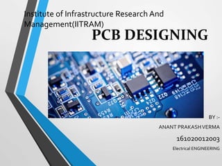
1. PCB DESIGNING
BY :-
ANANT PRAKASHVERMA
161020012003
Electrical ENGINEERING
Institute of Infrastructure Research And
Management(IITRAM)
2. History of Printed Circuit Board
• First working device to use a printed circuit board (PCB) was
radio, invented by Paul Eisler. in 1942.
• First double sided PCB were produced in 1947.
• In 1960 multi layer-production began (4+ layer)
• In 2010 PCB production became multi-billion dollar market.
3. Introduction to a Printed Circuit Board
• A printed circuit board (PCB) :mechanically supports and electrically
connects, electronic components using conductive tracks, pads and other
features etched from copper sheets laminated onto a non-
conductive substrate. Components are generally soldered on PCB.
• PCB's can be single sided (one copper layer), double sided (two copper
layers) or multi-layer.
• A PCB populated with electronic components is called a printed circuit
assembly (PCA), printed circuit board assembly or PCB assembly (PCBA)
• Manufacturing circuit with PCB
is cheaper and faster.
4. What PCB is made of
• A basic PCB starts with a copper-clad fiberglass material
or thin copper sheets attached to either side of the board. It
consist of :-
Copper Foil
Copper Plating
Solder Flow
Solder Mask
Trace
Slots and Cut-outs
5. PCB CHARACTERISTICS
• Through-hole technology
The first PCBs used through-hole technology, mounting electronic
components by leads inserted through holes on one side of the board
and soldered onto copper traces on the other side. Boards may be
single-sided, with an un plated component side, or more compact
double-sided boards, with components soldered on both sides
6. PCB CHARACTERISTICS (cont.)
•Surface-mount technology
Surface-mount technology emerged in the 1960s, gained
momentum in the early 1980s and became widely used by the mid-
1990s. Components were mechanically redesigned to have small
metal tabs or end caps that could be soldered directly onto the PCB
surface, instead of wire leads to pass through holes
7. FABRICATION
Following are the basic steps of PCB design.
• Imaging
• Panelization
• Depaneling
• Etching
• Drilling
• Assembly
• Electrical Test
8. FABRICATION (cont.)
• Imaging : before manufacturing the
PCB fabrication data is generated by
computer aided design(CAD),
such as Siemens-NX, Autodesk, etc.
This data is read into the CAM(Computer Aided Manufacturing)
9. FABRICATION (cont.)
• Panelization : It’s a procedure whereby a number of PCBs
grouped for manufacturing onto a larger board(panel). There
are two type of panels
1. Assembly panel
2.Bare- Board manufacturing panel
10. FABRICATION (cont.)
• Depaneling: The panel is eventually broken into individual
PCBs. Its done by lasers it cuts the panel and reduce stress on
circuit board
• Copper Patterning : This step is to replicated the pattern on
copper foil. Subsequent etching removes the unwanted copper.
Some of the technique used for hybrid circuit.
1. Silk screen printing .
2. Photoengraving .
3. PCB milling .
4. CNC laser plotter.
11. FABRICATION (cont.)
Etching process
Chemical etch
• Chemical etching is usually done with
ammonium per sulphate or ferric chloride.
• For PTH (plated-through holes), additional steps of electroless
deposition are done after the holes are drilled, then copper is
electroplated to build up the thickness, the boards are screened,
and plated with tin/lead. The tin/lead becomes the resist leaving
the bare copper to be etched away.
Cont.…
12. FABRICATION (cont.)
Laser Etch
• A new process creating new standards and the demise of the
chemical process is plasma etch. In addition to no etch-back,
this process also eliminates imaging, or film error using a
direct imaging process, which transfers the layer image directly
to the material
13. FABRICATION (cont.)
• Drilling: Holes through a PCB are typically drilled with small
diameter drill bits made of tungsten carbide. Drilling is generally
performed by automated drilling machines.
• Assembly: In this step the board is
filled with electronic component ,using
variety of soldering techniques this is
known as printed circuit board assembly
(PCBA).
14. Industry Applications of PCB
• Automotive Industry
• Medical Industry
• Defence
• Scientific Instrumentation
• Broadcasting
• Power management
• Retail Industry
….etc.
15. Power supply board
• A power supply is a device that supplies electric power to
an electrical load.
• Power converters that convert one form of electrical energy
to another.
• Power supplies for electronic devices can be broadly divided
into two type
1. Linear power supplies
2. Switching power supplies.
16. Power supply board (contd.)
• Linear power supplies:
Linear power converters process the input power directly, with all
active power conversion components operating in their linear
operating regions. Example our power meter.
• Switching power supplies:
The input power is converted to AC or to DC pulses before
processing, by components that operate predominantly in non-
linear modes (e.g., transistors)