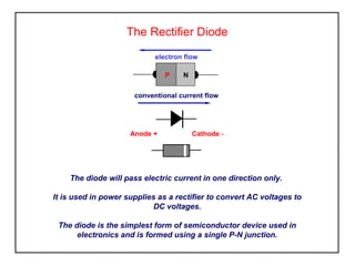
1. The Rectifier Diode
The diode will pass electric current in one direction only.
It is used in power supplies as a rectifier to convert AC voltages to
DC voltages.
The diode is the simplest form of semiconductor device used in
electronics and is formed using a single P-N junction.
conventional current flow
Cathode -Anode +
NP
electron flow
2. Simple Rectifier Circuit
The simplest rectifier circuit is called the ‘Half-Wave’ rectifier as it
only converts one half cycle.
Since current passes in one direction only, the negative portion of
the waveform is blocked.
0 t
+
-
Vo
Vi
I D
-
ac
mains
supply
+
Vi
Vo
dc
(unsmoothed)
voltage
VF
3. Rectifier Diode Characteristics
The rectifier diode has a low resistance in the forward direction and a very high
resistance in the reverse direction. It therefore passes current in one direction
only.
A diode which is reverse-biased will not pass a significant current, however if
the reverse voltage rating is exceeded the diode will break down. This voltage is
called the maximum reverse voltage (VRRM ).
VF
IF
(mA)
-IR
(µA)
Forward
bias
VR
0.4 0.6
Reverse
bias
breakdown
Voltage
(VRRM )
silicon
germanium
4. The Rectifier Diode – Characteristics
Activity
Silicon Diode (1N4001)
Select your components and instruments place them on the breadboard.
Connect the components to form the circuit shown using link wire.
Set power supply voltage to 15 volts
Adjust current from 0 to 20mA in 2mA steps and record your results
Germanium diode (OA91)
Repeat the above for the germanium diode.
R1
470Ω
DC POWER
SUPPLY
15V
VR1
1kΩ
VF
Multi-meter set to
volts
(2V)
+
+
IF
Objective: To measure and compare the characteristics of a silicon and
germanium rectifier diode.
R1
470Ω+
-
TEST
DIODE
Multi-meter set to
current
(100mA)
5. The Rectifier Diode – Characteristics Activity
Breadboard layout and Connections
Select your components and instruments place them on the breadboard
as shown and connect the test instruments.
Ammeter
IF
-+Voltmeter
VF
+ -
DC Power
Supply
+
15v
R1
470Ω
VR1
1kΩ
- TEST
DIODE
6. The Zener Diode
The Zener diode is a silicon junction diode designed to operate in the
reverse conduction mode and provide a stable voltage across its terminals.
It is used to provide a reference voltage in comparator circuits, power
supply circuits and constant current sources.
It can also be used to provide a regulated supply to a load but has
limitations where the load can change.
conventional current flow
Cathode +Anode -
7. Zener Diode Applications
The zener diode provides a stable voltage (VZ) from a varying source voltage (VI).
Circuit analysis
ILOAD
IZ
R
+
-
+
-
VZ
IT
VI
VR
IT = IZ + IL amps ohmsR =
VI - VZ
IT
VR = VI - VZ volts
R
+
-
+
-
Regulated (Fixed)
output voltage,
(VO )
Unregulated
input voltage
(VI )
Typical application
8. Zener Diode Characteristics
The zener diode will pass electric current in both directions, however it is
usually operated in the reverse bias mode.
Its resistance is high in the ‘reverse’ direction until the zener breakdown voltage
(VZ ) is reached. At this point the diode conducts as its resistance becomes very
low, maintaining a constant voltage across its terminals.
VF
IF
(mA)
-IR
(mA)
Forward
bias
VR 0.6V
Reverse
bias
Zener breakdown
Voltage
(VZ )
Breakdown
current
(IZ )
9. Diode Types and Markings
Diode types range from small signal glass and general purpose ceramic to high
current stud mounted.
Applications include power supply rectifiers, protection and detector circuits
for radio tuning.
Diodes are identified using an alphanumeric code and the cathode is identified
by a bar.
Package styles range from miniature glass bead to large metal stud. Stud
mounted styles print the diode symbol orientated to identify the polarity.
1 watt rectifier
diode
30 watt rectifier
diode
Germanium
signal diode
10. The PN Junction
A p-n junction is a piece of semiconductor material in which part of the material is p-type
and part n-type.
At the junction donated electrons called majority carriers diffuse into the p-type material
and the acceptor holes diffuse into the n-type material
The area in the region of the junction becomes depleted of holes and electrons due to
re-combination and is called the depletion layer.
Impurity atoms
(fixed)
p - type material n - type material
Holes
(mobile carriers)
Electrons
(mobile carriers)
Electrons
(negative charge carriers)
Holes
(positive charge carriers)
Depletion layer