
Empfohlen
Weitere ähnliche Inhalte
Was ist angesagt?
Was ist angesagt? (20)
Andere mochten auch
Ähnlich wie Electronics power supplies
Ähnlich wie Electronics power supplies (20)
Mehr von sdacey
Mehr von sdacey (13)
Kürzlich hochgeladen
Kürzlich hochgeladen (20)
Electronics power supplies
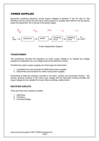
- 1. POWER SUPPLIES Equipment containing electronic circuits require voltages of between 5 and 30 volts dc. We therefore need to convert the 240 volt ac mains supply to a suitable value before it can be used to power the equipment, this is the job of the power supply. TRANSFORMER The transformer converts the hazardous ac mains supply voltage to an isolated low voltage suitable for rectification into a dc voltage used by the electronic circuits. Transformers used in power supplies are of two types of construction, 1. Laminated iron core and bobin for 50Hz linear power supplies. 2. Solid ferrite core and bobin for switch mode power supplies. Comprising at least two windings mounted in the bobin, primary and secondary winding. The primary winding connects to the mains input voltage and the secondary winding provides the output voltage and are isolated from each other providing a safety barrier. RECTIFIER CIRCUITS There are three main classes of rectifier, 1. Half-Wave. 2. Full-Wave. 3. Full-Wave Bridge. electronics-powersupplies-130517160825-phpapp02.doc Page 1 transformer rectifier smoothing circuit stabilizing circuit dc output ac input Power Supply Block Diagram
- 2. Half Wave Rectification During the first half cycle diode D conducts since its anode is positive with respect to it cathode. During the second half cycle its anode is negative with respect to the cathode and the diode blocks the flow of current. Therefore only the positive half cycles will be available to the load at the frequency of the mains supply. The voltage Vo will have an amplitude equal to the peak value of the secondary voltage Vi minus one diode volt drop (0.7V), however only half the power will be available due to the missing half cycle of the negative part of the input voltage. Assuming the secondary voltage Vi to be 12V rms then Vo will be, electronics-powersupplies-130517160825-phpapp02.doc Page 2 I D Vi Vo 0 time + - - Vi Vo ac mains R + Half-Wave VVVV Dio 268.167.0)12414.1(2 =−×=−×=
- 3. Full Wave Rectification The full wave rectifier circuit uses two diodes and a transformer with a centre-tapped secondary. With the centre tap being the reference point at 0V, then when A is at its positive peak B will be at its negative peak diode D1 will conduct. When A is at its negative peak B will be at its positive peak and diode D2 will conduct. In full wave rectification both halves of every cycle of input voltage are available to the load at a frequency of twice the supply frequency. This circuit consists of two half-wave rectifiers supplying the load on alternate half cycles of input voltage Vi. The voltage Vo will have an amplitude equal to the peak value of the secondary voltage Vi minus one diode volt drop (0.7V), however double the power of the half-wave version will be available due to the additional half cycle from the negative part of the input voltage. Assuming the secondary voltage Vi to be 12V rms then Vo will be, electronics-powersupplies-130517160825-phpapp02.doc Page 3 VVVV Dio 268.167.0)12414.1(2 =−×=−×= B - time Vi Vo 0 + - + Vi ac mains D2 D1o RVo Full-Wave A I I
- 4. Full Wave Bridge Rectification The full wave bridge rectifier circuit uses four diodes and, for a single rail output, an untapped transformer secondary. When A is at its positive peak B will be at its negative peak diodes D1 and D2 will conduct. When A is at its negative peak B will be at its positive peak and diodes D3 and D4 will conduct. In full wave rectification both halves of every cycle of input voltage are available to the load at a frequency of twice the supply frequency. The voltage Vo will have an amplitude equal to the peak value of the secondary voltage Vi minus two diode volt drops(1.4V), due to the current path through out going and return. As with the half- wave the output will fluctuate at twice the mains frequency. Assuming the secondary voltage Vi to be 12V rms then Vo will be, electronics-powersupplies-130517160825-phpapp02.doc Page 4 Vi Vo ac mains D2 D3 D1D4 R Full-Wave Bridge time Vi Vo 0 + - A B VVVV Dio 57.154.1)12414.1(2 =−×=−×=
- 5. Dual Rail Output An adaptation of the full-wave bridge circuit is that of the dual rail power supply commonly used to power analogue electronic systems and computer circuits since they usually require both positive and negative supply rails. With the addition of a centre-tapped secondary two supply rails can be achieved using the centre tap as the 0V reference. Smoothing Circuits The varying dc output voltage from the rectifier although adequate for charging a battery is not suitable for electronic equipment and must be smoothed to a steady dc level. The simplest way to obtain a smoothed output is to connect a high value capacitor across it, called a reservoir capacitor. Its value can range from 100μF to 10,000μF depending on the current and smoothing required. electronics-powersupplies-130517160825-phpapp02.doc Page 5 -Vi R D2 + - 0V +Vo ac mains D3 D1 D4 B A -Vo R +Vi Dual Rail Power Supply Positive Output Negative Output time Vi Vo 0 + - time0 + Vi - Vo
- 6. During the part of the positive half-cycle C is charging to near the peak value of the ac secondary voltage. During the rest of the cycle C is supplying the load by partly discharging into it and Vo falls until the next half-cycle tops up the charge on C. The small variation in the smoothed dc output is called the ripple voltage and in the half-wave has the same frequency as the mains supply. Since the half-wave uses only the positive half-cycles the discharge period is twice as long as the full-wave causing the ripple voltage to be greater. Capacitor and Diode Ratings Capacitor. The smoothing action of the reservoir capacitor is due to its large capacitance making the time constant CR large, (R is the resistance of the load), compared with the time for one cycle of ac mains. The larger C is the better the smoothing but the peak charging current pulses are greater. electronics-powersupplies-130517160825-phpapp02.doc Page 6 Connection of Reservoir Capacitor I D - Vi Vo ac mains R + C C charging C discharging 0 time VO - Half-Wave Output 0 time Vo C charging C discharging Full Wave output
- 7. The capacitor should have a voltage rating at least equal to the peak value of the transformer secondary voltage at maximum line input. Diode. Consideration must be given to the peak inverse voltage which is the maximum voltage the diode can block when reverse biased and should be at least twice the peak to peak value of the transformer secondary voltage at maximum line input. Also the peak current rating must be greater than that required by the reservoir capacitor during charging. Stabilizing Circuits The circuits discussed have one major draw back in that they do not provide any form of control on the output voltage which can change with mains and load variation, To overcome this and provide a stable output voltage of a known value we need to add a stabilizing circuit, or regulator. electronics-powersupplies-130517160825-phpapp02.doc Page 7 dc output load bad good Load Regulation
- 8. Zener Diode Regulator A basic form of regulator can be achieved using a zener diode and a resistor to limit the zener current. When a zener diode is reverse biased the voltage across it is almost constant. This property can be used to provide a stable voltage for a wide range of input voltage. The total current I is divided between the zener current IZ and the load current IL. Since R and VZ are constant then I is constant, if IL reduces due to increase in RL then IZ will increase by the same amount. At IL = 0, then IZ = I, the zener diode must has the power rating to safely carry this current. Zener Diode Power rating, and Maximum Current rating, electronics-powersupplies-130517160825-phpapp02.doc Page 8 + - R IL VL Z RL IZ I Vi Zener Diode Regulator I VV R Zi − =LZ III += and Z ZZ V P I IVP max max max = =
- 9. Transistor Regulator Adding a transistor to the zener diode circuit will remove the problems associated with the simple zener regulator since the zener current is constant, neglecting small variations in IB. Also the load current capability is increased by the HFE of the transistor. Type No Pol. Vce (V) Ic (max) PTOT hFE (min) Case BD135 npn 45 1.5A 12.5W 40@1.5A TO-126 BD136 pnp 45 1.5A 12.5W 40@1.5A TO-126 TIP31A npn 60 3A 40W 10@1A TO-220 TIP32A pnp 60 3A 40W 25@1A TO-220 2N3055 npn 60 15A 117W 20@4A TO-3 TIP2955 pnp 100 15A 90W 20@4A TO-218 electronics-powersupplies-130517160825-phpapp02.doc Page 9 VZ -VBEI Zener Stabilized Transistor Regulator IB IZ +IB VO VI RL IL VZ Example of Power Transistor Data
- 10. Integrated Circuit Voltage Regulator Integrated circuit voltage regulators are available as three terminal devices with internal protection from overload and overheating. They are available in both positive and negative fixed voltages from ±5 to ±15 volts with current ratings from 100mA to 3 Amps. These devices have complex internal circuitry and should be mounted on a heat sink to ovoid overheating and thermal shutdown. Type No Voltage Current Polarity Style 78L, 05, 12, 15 5, 12, 15 100mA positive TO92 79L, 05, 12, 15 5, 12, 15 100mA negative TO92 78, 05, 12, 15 5, 12, 15 1A positive TO220 79, 05, 12, 15 5, 12, 15 1A negative TO220 78S, 05, 12, 15 5, 12, 15 2A positive TO220 LM323K 5 3A positive TO3 LM387A 5 500mA positive TO220 LM338T 1.2 – 37 variable 5A positive TO3 LM337T 1.2 – 37 variable 5A negative TO3 Heatsinks A common method of voltage regulation in linear power supplies uses either a transistor or three terminal regulator to control the output voltage. The process of regulation dissipates power, which, in turn generates heat within the regulation device. To remove this heat quickly and efficiently the regulator is mounted on a heatsink. electronics-powersupplies-130517160825-phpapp02.doc Page 10 Example of Heat Sinks Integrated Circuit Regulator RL ac mains Vi Vo 7805 Heat Sink Common types of Voltage Regulator
- 11. Heat sinks are manufactured from aluminium and usually painted black so as to dissipate the heat energy more efficiently and prevent overheating. They are rated in degrees per watt known as the thermal resistance. For example a 2°CW-1 the temperature of the heatsink rises by 2°C above its ambient temperature for every watt of power it has to remove. To dissipate 10W, the rise will be 20°C. Switch Mode Power Supplies The power supplies described so far are known as linear power regulators since they operate on a stable dc level and the control voltage is a continuously varying level. Although cost effective and simple in their design and operation they are bulky and inefficient, as low as 50% and requiring large heatsinks on the regulator. Switch mode supplies work by chopping the dc level at a high frequency, 100 – 200kHz using fast switching transistors and then pass this to a small high frequency ferrite cored transformer. The switching frequency is pulse width modulated meaning that the ratio of ‘on’ time to ‘off’ time electronics-powersupplies-130517160825-phpapp02.doc Page 11
- 12. changes as the load or line input changes. These power supplies although complex in their design are much smaller than the linear types and up to 85% efficient. electronics-powersupplies-130517160825-phpapp02.doc Page 12 Example of Switch Mode Power Supply (SMPS)