
Empfohlen
Weitere ähnliche Inhalte
Was ist angesagt?
Was ist angesagt? (20)
Ähnlich wie Working of capacitive SAR ADC
Ähnlich wie Working of capacitive SAR ADC (20)
Kürzlich hochgeladen
Kürzlich hochgeladen (20)
Working of capacitive SAR ADC
- 2. SAR ADC Introduction Charge-redistribution Converter Sample Mode Hold Mode Redistribution Mode 2
- 3. A successive approximation ADC is a type of analog-to-digital converter that converts a continuous analog waveform into discrete digital representation via binary search SAR ADC circuit typically consists of four chief sub circuits: A sample and hold circuit to acquire the input voltage (Vin). An analog voltage comparator that compares Vin to the output of the internal DAC and outputs the result of the comparison to the successive approximation register (SAR). A successive approximation register sub circuit designed to supply an approximate digital code of Vin to the internal DAC. An internal reference DAC that supplies the comparator with an analog voltage equivalent of the digital code output of the SAR for comparison with Vin. 3
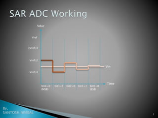
- 4. SAR is initialized with MSB equal to a digital 1. This code is fed into the DAC, which then supplies the analog equivalent of this digital code (Vref/2) into the comparator circuit for comparison with the sampled input voltage. If this analog voltage exceeds Vin the comparator causes the SAR to reset this bit; otherwise, the bit is left 1. Then the next bit is set to 1 and the same test is done, continuing this binary search until every bit in the SAR has been tested. The resulting code is the digital approximation of the sampled input voltage and is finally output by the DAC at the end of the conversion (EOC). Figure 0. SAR ADC block diagram 4
- 5. Figure 1 shows the simplified circuit of a 5-bit charge redistribution converter using switched capacitor architecture All capacitors have binary weighted values, i.e., C, C/2, C/4,….C/2n–1. The last two capacitors having the value C/2n–1 are connected so that the total capacitance of the n+1 capacitors is 2C 5
- 6. The conversion process is performed in three steps: the sample mode, the hold mode, and the redistribution mode (in which the actual conversion is performed). Sample mode In the sampling mode (Figure 2), switch SA is closed and SB is switched to the input voltage Vin. The remaining switches are turned to common bus B. Due to charging, a total charge of Qin = –2C x Vin is stored on the lower plates of the capacitors. 6
- 7. Hold mode During the hold mode (Figure 3), switch SA is opened while the switches S4….S0 are connected to ground, thereby applying a voltage of Vc = –Vin to the comparator input. This means that the circuit already has a built-in sample-and-hold element. 7
- 8. Redistribution mode The actual conversion is performed by the redistribution mode. The first conversion step, shown in Figure 4, connects C (the largest capacitor) via switch S4 to the reference voltage Vref Capacitor C forms a 1:1 capacitance divider with the remaining capacitors connected to gnd. Comparator input voltage becomes Vc = –Vin + Vref/2 If Vin > Vref /2, then Vc < 0, comparator output goes high, providing the most significant bit MSB (bit 4) = 1. On the other hand, if Vin < Vref /2, then Vc > 0, and bit 4 = 0. 8
- 9. The second conversion step connects C/2 to Vref . If the first conversion step resulted in bit 4 = 1, switch S4 is turned to ground again to discharge C as shown in Figure 5 resulting in a comparator input voltage Vc = -Vin + Vref/4 Otherwise it remains connected to Vref if bit 4 = 0 (Figure 6), resulting in a comparator input voltage Vc = -Vin + 3Vref/4 9
- 10. According to this voltage, the next most significant bit (bit 3) is obtained by comparing Vin to 1/4 Vref or 3/4 Vref through the different voltage dividers. Switch S3 is then either turned to ground if bit 3 = 1, thereby discharging C/2, or S3 remains connected to Vref if bit 3 = 0. This process continues until all bits are generated, with the final conversion step being performed at a comparator input voltage of Vc = –Vin + bit4 x Vref/2 + bit3 x Vref/4 + bit2 x Vref/8 + bit1 x Vref/16 + bit0 x Vref/32 10
- 11. 11