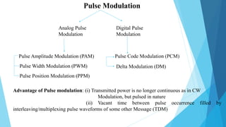
1. Pulse Modulation
Analog Pulse
Modulation
Digital Pulse
Modulation
Pulse Amplitude Modulation (PAM)
Pulse Width Modulation (PWM)
Pulse Position Modulation (PPM)
Pulse Code Modulation (PCM)
Delta Modulation (DM)
Advantage of Pulse modulation: (i) Transmitted power is no longer continuous as in CW
Modulation, but pulsed in nature
(ii) Vacant time between pulse occurrence filled by
interleaving/multiplexing pulse waveforms of some other Message (TDM)
2. Sampling Theorem
This provides a mechanism for representing a continuous time signal by a discrete time signal ,
taking sufficient number of samples of signal so that original signal is represented in its samples
completely. It can be stated as:
(i) A band-limited signal of finite energy with no frequency component higher than fm Hz, is
completely described by its sample values which are at uniform intervals less than or equal to 1/2fm
seconds apart. [Ts=
𝟏
𝟐𝒇𝒎
]where Ts is sampling time.
(ii) Sampling frequency must be equal to or higher than 2fm Hz. [fs ≥ 2fm]
A continuous time signal may be completely represented in samples and recovered back, if fs≥2fm,
where fs is sampling frequency and fm is maximum frequency component of message signal
3. Proof of sampling theorem
Sampling of input signal x(t) can be obtained by
multiplying x(t) with an impulse train δ(t) of
period Ts.
The output of multiplier is a discrete signal called
sampled signal which is represented with y(t) in
the diagrams,
y(t)=x(t).δ(t)......(1)
The Fourier series representation of δ(t) :
δ(t)=a0+Σ∞ (ancosnωst + bnsinnωst)......(2)
n=1
where a0=
1
𝑇 𝑠
∫ δ(t) dt =
1
𝑇𝑠
δ(0) =
1
𝑇 𝑠
an=
2
𝑇 𝑠
∫δ(t)cosnωsdt =
2
𝑇 𝑠
δ(0)cosnωs0=
2
𝑇 𝑆
bn=
2
∫δ(t)sinnωst dt =
2
δ(0)sinnωs0=0
T/2
-T/2
-T/2
5. Y(ω)=
𝟏
𝑻 𝑺
−∞
+∞
𝑿(𝝎 − 𝒏𝝎 𝒔)
To reconstruct x(t), one has to recover input signal spectrum X(ω) from sampled signal spectrum Y(ω),
which is possible when there is no overlapping between the cycles of Y(ω) which is possible if
fs≥2fm
For fs=2fm, is known as Nyquist rate.
Ts =
𝟏
𝟐𝒇𝒎
is known as Nyquist interval
Aliasing Effect
The overlapped region in case of under sampling
represents Aliasing effect. It can be termed as “the phenomenon of a high-frequency component in the
spectrum of a signal, taking on the identity of a lower-frequency component in the spectrum of its
sampled version.
This effect can be removed by considering
(i) fs >2fm or
(ii) by using anti aliasing filters which are low pass filters and eliminate high frequency components
6. Three types of sampling techniques:
Impulse sampling: Obtained by multiplying input signal x(t) with impulse train of period 'Ts.
Also called ideal sampling. Practically not used because pulse width cannot be zero and the generation
of impulse train not possible.
7. Natural sampling
This type of sampling similar to ideal
sampling except for the fact that instead of
delta function, now we use rectangular train
of period Ts. i.e. multiply input signal x(t) to
pulse train
An electronic switch is used to periodically
shift between the two contacts at a rate of
fs = (1/Ts ) Hz, staying on the input contact
for C seconds and on the grounded contact for
the remainder of each sampling
The output xs(t) of the sampler consists of
segments of x(t) and hence Xs(t) can be
considered as the product of x(t) and
sampling function s(t).
Xs(t)= x(t)×s(t)
8. Using Fourier series, we can rewrite the signal S(t) as:
S(t)= C0+ 𝑛=1
∞
2𝐶𝑛𝑐𝑜𝑠(𝑛ω 𝑠 𝑡)
Where the Fourier coefficients C0=
𝝉
𝑻 𝒔
and Cn=fsτsinc(nfsτ)
Therefore: xs(t)=x(t)[C0+ 𝑛=1
∞
2𝐶𝑛(𝑐𝑜𝑠𝑛𝜔 𝑠 𝑡)]
xs(t)=C0x(t)+2C1x(t) cos(ωst)+2C2x(t) cos(2ωst)+……
Applying Fourier Transform for the above equation
Using x(t)↔X(f)
x(t) cos(2πf0t)↔
𝟏
𝟐
[X(f-f0)+X(f+f0)]
Xs(f)=C0X(f)+C1[X(f-f0)+X(f+f0)]+C2[X(f-f0)+X(f+f0)]+…………
Xs(f)= C0X(f)+ 𝒏=−∞
∞
𝑪 𝒏 𝑿(𝒇 − 𝒏𝒇𝒔)
Xs(f) = Aτ/ Ts .[ Σ sin c(n fs.τ) X(f-n fs)]
The signal Xs(t) has the spectrum which consists of message spectrum and repetition of message
spectrum periodically in the frequency domain with a period of fs. But the message term is scaled by
‘Co”( sinc function) which is not the case in instantaneous sampling.
9.
10. Flat Top sampling: During transmission, noise is introduced at top of the transmission pulse
which can be easily removed if the pulse is in the form of flat top.
Here, the top of the samples are flat i.e. they have constant amplitude and is equal to the
instantaneous value of the baseband signal x(t) at the start of sampling. Hence, it is called as flat
top sampling or practical sampling.
Flat top sampling makes use of sample and hold circuit
Theoretically, the sampled signal can be obtained
by convolution of rectangular pulse h(t) with
ideally sampled signal ,sδ(t)
g(t)= s(t) ⊗ h(t)
δ(t)
t
h(t)
⊗ =
0 τ
f(t) ⊗ δ(t) = f(t); property of delta function
Applying a modified form; s(t) in place of δ(t)
11. On convolution of s(t) and h(t), we get a pulse whose duration is equal to h(t) only but amplitude
defined by s(t).
Train of impulses given by:
δTs(t) = 𝒏=−∞
∞ 𝜹(𝒕 − 𝒏𝑻𝒔)
Signal s(t) obtained by multiplication of message signal x(t) and δTs(t)
Thus, s(t) = x(t). δTs(t)
s(t)= 𝒏=−∞
∞
𝒙(𝒏𝑻𝒔)𝜹(𝒕−𝒏𝑻 𝒔)
Now sampled signal g(t) given as:
g(t)=s(t) ⊗ h(t) G(f)=S(f) H(f)
= −∞
∞
𝑠 τ ℎ 𝑡 − τ 𝑑τ S(f)=fs 𝑋(𝑓 − 𝑛𝑓𝑠)
g(t) = −∞
∞
𝑛=−∞
∞
𝑥(𝑛𝑇𝑠)δ(τ-nTs) h(t-τ)dτ
g(t)= −∞
∞
𝒙(𝒏𝑻𝒔) −∞
∞
𝜹(𝝉 − 𝒏𝑻 𝒔) 𝒉(𝒕 − 𝝉)𝒅𝝉
Using shifting property of delta function: −∞
∞
𝑓(𝑡)δ(𝑡 − 𝑡𝑜)=f(t0)
g(t)= −∞
∞ 𝒙 𝒏𝑻 𝒔 𝒉(𝒕 − 𝒏𝑻𝒔)
G(f)=fs −∞
∞ 𝑿 𝒇 − 𝒏𝒇𝒔 𝑯(𝒇) Spectrum of flat top samples
12. Aperture Effect: Spectrum of flat topped sample is given by;
G(f)=fs ∑〖𝑿(𝒇−𝒏𝒇 𝒔)𝑯(𝒇)〗 , where H(f)= τ.sin c(fs.t)𝒆^(−𝒋𝝅𝒇𝝉)
This equation shows that signal g(t) is obtained by passing the signal s(t) through a filter having
transfer function H(f).
Figure(a) shows one pulse of rectangular pulse train and each sample of x(t) i.e. s(t) is
convolved with this pulse
Figure (b) shows the spectrum of this pulse. Thus, flat top sampling introduces an amplitude
distortion in reconstructed signal x(t) from g(t). There is a high frequency roll off making H(f)
act like a LPF, thus attenuating the upper portion of message signal spectrum. This is known as
aperture effect
13. How to minimize aperture effect?? An equalizer at the receiver end is needed to compensate aperture
effect. The receiver contains low pass reconstruction Filter with cut off slightly higher than fm Hz.
Reconstruction
Filter
Equalizer
PAM
Signal
g(t)
Message signal
x(t)
Equalizer in cascade with reconstruction filter has the effect of decreasing the in band loss of
reconstruction filter, frequency increases in such away so as to compensate aperture effect.
Heq(f)=
𝑲.𝒆−𝒋𝟐𝝅𝒇𝒕𝒅
𝑯(𝒇)
,
where td is time delay introduced by LPF being equal to τ/2
Heq(f) =
𝑲
𝝉𝒔𝒊𝒏 𝒄(𝒇𝝉)
14. Pulse Amplitude Modulation (PAM)
Amplitude of the pulse carrier varies proportional to the instantaneous amplitude of the message
signal.
The width and positions of the pulses are constant in this modulation.
PAM could be:
(i)Single polarity PAM: A suitable fixed DC bias is added to the signal to ensure that all the pulses
are positive.
(ii) Double polarity PAM: In this the pulses are both positive and negative.
15.
16. Depending on type of sampling PAM can be:
(i) Ideal Sampling PAM, (ii) Natural sampling PAM and (iii) Flat top PAM.
The advantage of this modulation is the generation and detection is easy in this modulation and
also allows multiplexing.
The disadvantage is large band width of transmitted signal.
BPF characteristics
17. For a PAM signal produced with natural sampling, the sampled signal follows the waveform of
the input signal during the time that each sample is taken.
A PAM signal is generated by using a pulse train, called the sampling signal (or clock signal) to
operate an electronic switch or "chopper". This produces samples of the analog message signal.
The switch is closed for the duration of each pulse, allowing the message signal at that sampling
time to become part of the output.
The switch is open for the remainder of each sampling period making the output zero. This is
known as Natural PAM.
In simplest form PAM can be visualized as o/p of an
AND gate whose two inputs are message signal x(t)
and pulses at sampling rate
.
18. For flat-top sampling, a sample-and-hold circuit is used in conjunction with the chopper to hold
the amplitude of each pulse at a constant level during the sampling time,
Flat-top sampling, produces pulses whose amplitude remains fixed during the sampling time.
The amplitude value of the pulse depends on the amplitude of the input signal at the time of
sampling.
Aperture Effect seen in this type of PAM. Equalizers used at receiver end
Transmission Bandwidth in PAM
𝝉 ≪ Ts
fs≥ 𝟐𝒇𝒎 ; 𝑻𝒔 ≤
𝟏
𝟐𝒇𝒎
𝝉≪ Ts≤
𝟏
𝟐𝒇𝒎
If on and off time of PAM pulse is same then fmax=
𝟏
𝟐𝝉
BW≥ 𝒇𝒎𝒂𝒙; 𝑩𝑾 ≥
𝟏
𝟐𝝉
𝑩𝑾 ≥
𝟏
𝟐𝝉
≫ fm
19. Transmission of PAM signals
For PAM signals to be transmitted through space using antennas, they must be amplitude/
frequency/ phase modulated by a high frequency carrier and only then they can be transmitted.
Thus the overall system is PAM-AM. PAM-FM or PAM-PM and at receiving end, AM/ FM/PM
detection is first employed to get the PAM signal and then message signal is recovered.
Drawbacks of PAM
Bandwidth required for transmission of PAM signal is very large in comparison to maximum
frequency present in modulating signal.
Since amplitude of PAM pulses varies in accordance with modulating signal so interference of
noise is maximum in PAM
Variation of the peak power required by transmitter
20. Demodulation of PAM
PAM signal sampled at Nyquist rate can be reconstructed at the receiver end , by passing it
through an efficient Low Pass Filter (LPF) with exact cut off frequency of fs/2. This is
known as Reconstruction or Interpolation Filter.
The low pass filter eliminates the high-frequency ripples and generates the demodulated
signal. This signal is then applied to the inverting amplifier to amplify its signal level to have
the demodulated output with almost equal amplitude with the modulating signal
For a flat topped PAM, a holding circuit followed by a LPF gives demodulated signal
Holding
circuit
Received PAM
signal
21. C
Zero order Holding Circuit
Switch S closes after the arrival of pulse and opens at the end of pulse.
Capacitor C charges to pulse amplitude value and holds this value during interval between two pulses.
The sampled values are shown in fig.
Holding circuit o/p smoothened in LPF.
Known as zero order holding circuit, which considers only the previous sample to decide value between two
pulses
First order holding circuit considers previous two samples, second order holding circuit considers previous three
samples.
PAM
signal
22. Pulse Time modulation
Generation of PTM signals can be either by:
(i) Indirect Method: Firstly PAM signals are generated, Synchronized is generated during each pulse
interval. These two signals are added and the sum is applied to a comparator whose reference level is
suitably chosen. The second crossing of comparator level used for PPM
(ii) Direct method: PTM waveforms generated without using PAM waveforms
Pulse Width modulation
The pulse width modulation is the modulation of signals by varying the width of pulses. The amplitude and
positions of the pulses are constant in this modulation
In PTM, amplitude of pulse is constant while position or width of pulse is made proportional to
the amplitude of the signal at the sampling instant.
It can be PWM and PPM
In both the cases amplitude constant and does not carry information so amplitude limiters can be
used ( like in FM) providing good noise immunity
24. The non inverting input of the comparator is fed by the input message or modulating signal x(t)
and the other input by a saw-tooth signal which operates at carrier frequency.
The comparator compares the two signals together to generate the PWM signal at its output. Its o/p is
high only when the instantaneous value of x(t) is higher than sawtooth waveform.
The rising edges of the PWM signal occurs at the fixed time period (kTs) while trailing edge depends
on amplitude of message signal x(t).
When saw-tooth voltage waveform greater than x(t), o/p of comparator is zero, trailing edge is
modulated
If saw-tooth. waveform is reversed, trailing edge is fixed while leading edge is modulated.
Replacing saw-tooth waveform by triangular, both leading and trailing edge modulated.
(symmetrical PWM)
The amplitude of PDM/PWM will be positive saturation of the comparator shown as ‘A’, being same
for all pulses,
25. Three types of pulse-width modulation (PWM) are possible:
The leading edge of the pulse being constant, the trailing edge varies according to the message
signal.
The trailing edge of the pulse being constant, the leading edge varies according to the message
signal
The center of the pulse being constant, the leading edge and the trailing edge varies according
to the message signal (Symmetrical PWM)
26. Indirect Method:
Modulating signal (A) applied to i/p of PAM circuit [s(t) pulse train] and PAM signal generated(B).
S(t) also is i/p to Ramp generator(Integrator circuit), all having equal slopes, amplitude and
generation(D). These ramp pulses added to PAM pulses to produce varying height samples. These
varying height ramp gates a S.T ckt to generate varying width rectangular pulses of PWM.
PWMSummer
Schmitt
Trigger
Ramp
Generator
x(t)
A
PAM
generator
B
C
D
E F
27. PWM detector
Schmitt
Trigger
Ramp
Generator
Synchronization
Pulse generator
Adder
Level
Shifter
Rectifier LPF
1
2
3 4 5 6
Received PWM signal applied to ST circuit to remove noise
Regenerated PWM applied to Ramp generator
and synchronization pulse.
Heights of Ramp proportional to width of pulses.
Pulse generator produces reference pulses with constant
amplitude and width but delayed by specific amount.
Delayed reference pulses added to o/p of ramp generator
The o/p given to level shifter, negative offset shifts
waveform. Then clipped by rectifier followed by LPF to
give message signal.
Noisy PWM
28. Pulse position modulation
(PPM) is an analog modulating scheme in which the amplitude and width of the pulses are kept constant, while
the position of each pulse, with reference to the position of a reference pulse varies according to the
instantaneous sampled value of the message signal.
The transmitter has to send synchronizing pulses (or simply sync pulses) to keep the transmitter and receiver in
synchronism. These sync pulses help maintain the position of the pulses.
PPM is done in accordance with the PWM signal.
PWM signal is used as the trigger input to a monostable multivibrator.
Its o/p remains zero until it is triggered on the trailing edge of PWM
O/P of monostable MV switches to positive saturation value A and remains high for fixed period then goes
low
Hence, the position of these pulses is proportional
to the width of the PWM pulses.
Advantage As the amplitude and width are constant
the power handled is constant
Disadvantage: Synchronization between Transmitter
and receiver is a necessity
29. The PDM is differentiated, and then rectified and shaped.
PPM carries exactly the same information as long as the position
of the clock pulses (leading edge) is well defined in the received
signal.
PPM is superior to PDM for message transmission, since the wide
pulses of PDM require more energy than PPM when transmitted
PPM is suited for communication in the presence of noise.
Very high peak narrow pulses can be transmitted and the pulse
position can be determined even when the noise level is high,
However, transmitting very narrow pulses requires a large band
width
When light is used as the media for transmitting analog signals,
PPM or PCM are the most suitable types of modulation because
the maximum power output in the modulated light source,
such as LED or LASER is achieved when it is pulsed at a very
low duty cycle.
In PPM, necessary to transmit a series of sync pulses at a much
lower repetition rate than the sampling pulses, to avoid
interference with original signal and/or minimise the number of
pulses transmitted in order to conserve transmission power
30. Transmission BW of PWM and PPM
Both PWM and PPM have DC value.
Both need a shrp rise time and fall time to preserve the message information
Rise time be very less than Ts i.e. tr≪ Ts
Transmission BW: BT ≥
𝟏
𝟐𝒕𝒓
BW higher than PAM
31. PAM
The amplitude of the pulse is proportional to the amplitude of modulating the signal.
Band width of transmitting channel depends on the width of the pulse
Instantaneous power of transmitter varies. Noise interference is high
Complex system. Similar to A.M.
PWM
Width of pulse is proportional to amplitude of modulating signal.
The Bandwidth of transmitting channel depends on rise time of the pulse.
Instantaneous power of transmitter varies. Noise interference is minimum.
Simple to implement Similar to F.M.
PPM
Relative position of pulse is proportional to amplitude of modulating signal.
The bandwidth of transmitting channel depends on the rise time of the pulse.
Instantaneous power remains constant. Noise interference is minimum.
Simple to implement. Similar to P.M.
32. Difference Between PAM, PWM, and PPM
Parameter PAM PWM PPM
Type of Carrier: Train of Pulses Train of Pulses Train of Pulses
Variable Characteristic : Amplitude Width Position
Bandwidth Requirement: Low High High
Noise Immunity: Low High High
Information Contained in: Amplitude Variations Width Variations Position Variations
Power efficiency (SNR) Low Moderate High
Transmitted Power Varies Varies Remains Constant
Need to transmit synchronizing pulses Not needed Not needed Necessary
Bandwidth depends on width of the pulse rise time of the pulse rise time of the pulse
Transmitter power Inst. power varies Instantaneous power varies with Constant
with amplitude of pulses width of the pulses
Complexity of generation and detection Complex Easy Complex
12 Similarity with other Modulation Systems Similar to AM Similar to FM Similar to PM
33. Q. For a PAM transmission of voice signal with fm=3kHz, calculate the transmission BW. Given that
fs=8kHz and the pulse duration τ=0.1Ts
Soln: Ts=
1
𝑓𝑠
= 125µs
τ=0.1Ts=0.1×125=12.5µs
BW≥
𝟏
𝟐𝝉
≥ 40 kHz
Q. For the above signal if rise time is 1% of pulse width, find minimum Tx BW for PWM and PPM?
Soln: tr=τ×0,01= 1.25x 10⁻⁷
BT≥
1
2𝑡 𝑟
≥ 4MHz
Thus BW of PWM/PPM much higher than PAM
34. Multiplexing
Multiplexing refers to the combination of information streams from multiple sources for
transmission over a shared medium .
Multiplexor is a mechanism that implements the concept. It permits hundreds or even thousands of
signals to be combined and transmitted over a single medium. De-multiplexing refers to the separation
of a combination, back into separate information streams .
Principle used
Each sender communicates with a single receiver
All pairs share a single transmission medium
Multiplexor combines information from the senders
for transmission in such a way that the de multiplexer
can separate the information for receivers.
Cost savings obtained using single channel to send
Multiple signals.
36. Frequency Division Multiplex (FDM): Separation of spectrum into smaller frequency.
Channel gets band of the spectrum for the whole time. Each signal allocated different frequency
band i.e, Multiple carriers used
Each message signal is limited to fm Hz.
Example: Multiplexing of telephonic signals from n subscribers
Telephonic message (BW=3kHz) and broadcast signal
limited to 5kHz. Without multiplexing if n channels transmitted,
Interference and no useful information.
In FDM, each baseband signal translated by Analog Modulation (AM/Angle) to different carrier
frequencies.
Each carrier separated from neighbouring by at least 2fm
Multiplexed signals can be transmitted over a common channel without interference.
At receiver, various carrier frequencies selected using BPF tuned to appropriate carrier frequencies
and demodulated by separate detector.
37. Advantages: No dynamic coordination needed and works also for analog signals
Disadvantages: Waste of bandwidth if traffic distributed uneven; inflexible;
FDM System
38. Time Division Multiplexing
Time Division Multiplexing (TDM) is the time interleaving of samples from several sources so
that the information from these sources can be transmitted serially over a single communication
channel.
At the Transmitter :Simultaneous transmission of several signals on a time-sharing basis.
Each signal occupies its own distinct time slot, using all frequencies, for the duration of the
transmission. Slots may be permanently assigned on demand
At the Receiver : Decommutator (sampler) has to be synchronized with the incoming waveform
In Pulse modulation techniques, there is a free space between any two consecutive pulses of a
signal. This free space between pulses can be occupied by pulses from other channel. This is
Time Division Multiplexing (TDM) and makes maximum utilization of transmission channel.
Applications of TDM: Digital Telephony, Data communications, Satellite Access, Cellular radio
41. The system shows TDM of ‘N’ PAM channels.
Each channel to be transmitted is passed through LPF to band limit its frequency to fm Hz ( W Hz)
Outputs of LPF are connected to the rotating sampling switch or commutator.
It takes sample from each channel per revolution and rotates at the rate of fs.
Function of commutator is two fold: (i) Taking narrow samples of each of N input messages at
rate 1/Ts (ii) To sequentially interleave N samples Inside a sampling interval Ts
The single signal composed due to multiplexing of input channels given to Transmission channel
If W or fm is highest signal frequency in the message signal: fs ≥ 2fmor 2W; Ts or 𝟏/𝐟𝐬≤𝟏/𝟐𝐟𝐦
Thus time interval Ts contains one sample from each input. It is called frame. If N input channels
multiplexed, each frame will have one sample from each of N channel's input
Spacing between two samples: 𝐓𝐬/𝐍
No. of pulses/sec=1/ spacing between two pulses=1/(𝑇𝑠/𝑁) =𝑁/𝑇𝑠
Ts=1/fs; No. of pulses per second=Nfs
The no. of pulses transmitted per second is called signalling rate of TDM ‘r’
r=Nfs; fs ≥2fm; r ≥2Nfm or r ≥2NW
Pulsed TDM passed through LPF to convert it to baseband signal whose BW given by half
signalling rate
B.W=𝒓/𝟐 = Nfm=NW; Minimum Transmission Bandwidth
At the receiver, decommutator separates the time multiplexed input channels which then
passed through reconstruction filter
42. Synchronization in TDM system
The time division multiplexing (TDM) needs synchronization between multiplexer and demultiplexer.
If synchronization is not there between multiplexer and demultiplexer, a bit going to one channel may
be received by the wrong channel.
Because of this reason, one or more synchronization bits are usually added to the beginning of each
frame called Markers (highest amplitude)
These bits are called framing bits (Marker pulse), allows the demultiplexer to synchronize with the
incoming stream so that that it can separate time slot accurately.
Because of the marker pulse, no of channels to be multiplexed reduced by 1
Marker Pulse
x1
x2
xN-1
43. Crosstalk and Guard Times
RF transmission of TDM needs further modulation
TDM signal converted to smooth modulating waveform by passing through a baseband filter
This filtering gives rise to inter-channel crosstalk which means individual signal sample amplitude
interfere with each other. Thus interference between adjacent TDM channels is crosstalk
This interference can be reduced by increasing distance between individual signal amplitudes
The minimum distance between individual signal samples to avoid crosstalk is called guard time.
Ideally communication channel over which TDM signal is transmitted should be infinite but in
practise has a finite BW, known as band limited channels
Whenever signal passed through band limited channel, shape of signal will change.
Whenever a PAM-TDM signal transmitted over band limited channel, signals corresponding to x1(t)
get mixed with x2(t) and this overlap causes crosstalk.
To keep cross talk below -30dB, Tg≥
𝟎.𝟓𝟓
𝐁𝐖
Thus, guard time required to avoid cross talk decreases with increase in BW
44. Transmission Bandwidth for ‘N’ PAM-TDM channels: Nfm
Where fm is the maximum frequency of baseband signal
Advantages:
Full available channel BW can be utilized.
TDM circuitry not very complex
Problem of cross talk not very severe
Disadvantages
Synchronization for proper operation
45.
46.
47.
48. Application of PWM
Although PWM is also used in communications, its main purpose is actually to control the power
that is supplied to various types of electrical devices, most especially to inertial loads such as
AC/DC motors.
Pulse-width modulation (PWM) is used for controlling the amplitude of digital signals in order to
control devices and applications requiring power or electricity. It essentially controls the amount
of power, in the perspective of the voltage component, that is given to a device by cycling the on-
and-off phases of a digital signal quickly and varying the width of the "on" phase or duty cycle.
To the device, this would appear as a steady power input with an average voltage value, which is the
result of the percentage of the on time. The duty cycle is expressed as the percentage of being fully
(100%) on.
A very powerful benefit of PWM is that power loss is very minimal. Compared to regulating
power levels using an analog potentiometer to limit the power output by essentially choking the
electrical pathway, thereby resulting in power loss as heat, PWM actually turns off the power output
rather than limits it. Applications range from controlling DC motors and light dimming to heating
elements.
49. This simple circuit based around the familiar NE555 or 7555 timer chip is
used to produced the required pulse width modulation signal at a fixed
frequency output. The timing capacitor C is charged and discharged by
current flowing through the timing networks RA and RB as we looked at in
the 555 Timer tutorial.
The output signal at pin 3 of the 555 is equal to the supply voltage
switching the transistors fully “ON”. The time taken for C to charge or
discharge depends upon the values of RA, RB.
The capacitor charges up through the network RA but is diverted around
the resistive network RB and through diode D1. As soon as the capacitor is
charged, it is immediately discharged through diode D2 and network RB
into pin 7. During the discharging process the output at pin 3 is at 0 V and
the transistor is switched “OFF”.
Then the time taken for capacitor, C to go through one complete charge-
discharge cycle depends on the values of RA, RB and C with the time T for
one complete cycle being given as:
50. The time, TH, for which the output is “ON” is: TH = 0.693(RA).C
The time, TL, for which the output is “OFF” is: TL = 0.693(RB).C
Total “ON”-“OFF” cycle time given as: T = TH + TL with the output frequency being ƒ = 1/T
With the component values shown, the duty cycle of the waveform can be adjusted from about 8.3% (0.5V) to about 91.7% (5.5V) using a
6.0V power supply. The Astable frequency is constant at about 256 Hz and the motor is switched “ON” and “OFF” at this rate.
Resistor R1 plus the “top” part of the potentiometer, VR1 represent the resistive network of RA. While the “bottom” part of the
potentiometer plus R2 represent the resistive network of RB above.
These values can be changed to suite different applications and DC motors but providing that the 555 Astable circuit runs fast enough at
a few hundred Hertz minimum, there should be no jerkiness in the rotation of the motor.
Diode D3 is our old favourite the flywheel diode used to protect the electronic circuit from the inductive loading of the motor. Also if the
motor load is high put a heatsink on the switching transistor or MOSFET.
Pulse width modulation is a great method of controlling the amount of power delivered to a load without dissipating any wasted power.
The above circuit can also be used to control the speed of a fan or to dim the brightness of DC lamps or LED’s. If you need to control it,
then use Pulse Width Modulation to do it.
![Sampling Theorem
This provides a mechanism for representing a continuous time signal by a discrete time signal ,
taking sufficient number of samples of signal so that original signal is represented in its samples
completely. It can be stated as:
(i) A band-limited signal of finite energy with no frequency component higher than fm Hz, is
completely described by its sample values which are at uniform intervals less than or equal to 1/2fm
seconds apart. [Ts=
𝟏
𝟐𝒇𝒎
]where Ts is sampling time.
(ii) Sampling frequency must be equal to or higher than 2fm Hz. [fs ≥ 2fm]
A continuous time signal may be completely represented in samples and recovered back, if fs≥2fm,
where fs is sampling frequency and fm is maximum frequency component of message signal](data:image/gif;base64,R0lGODlhAQABAIAAAAAAAP///yH5BAEAAAAALAAAAAABAAEAAAIBRAA7)