Nanochemistry lectures-part 1
•
1 gefällt mir•108 views

lectures on nanochemistry for BSc students

Empfohlen
Empfohlen
Weitere ähnliche Inhalte
Was ist angesagt?
Was ist angesagt? (20)
Ähnlich wie Nanochemistry lectures-part 1
Ähnlich wie Nanochemistry lectures-part 1 (20)
Kürzlich hochgeladen
Kürzlich hochgeladen (20)
Nanochemistry lectures-part 1
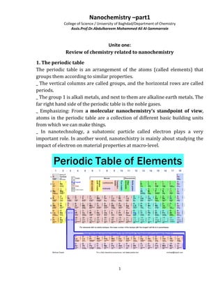
- 1. Nanochemistry –part1 College of Science / University of Baghdad/Department of Chemistry Assis.Prof.Dr.Abdulkareem Mohammed Ali Al-Sammarraie 1 Unite one: Review of chemistry related to nanochemistry 1. The periodic table The periodic table is an arrangement of the atoms (called elements) that groups them according to similar properties. _ The vertical columns are called groups, and the horizontal rows are called periods. _ The group 1 is alkali metals, and next to them are alkaline earth metals. The far right hand side of the periodic table is the noble gases. _ Emphasizing: From a molecular nanochemistry’s standpoint of view, atoms in the periodic table are a collection of different basic building units from which we can make things. _ In nanotechnology, a subatomic particle called electron plays a very important role. In another word, nanotechistry is mainly about studying the impact of electron on material properties at macro-level.
- 2. Nanochemistry –part1 College of Science / University of Baghdad/Department of Chemistry Assis.Prof.Dr.Abdulkareem Mohammed Ali Al-Sammarraie 2 2. Atomic structure Three major fundamental subatomic particles: electrons, protons and neutrons. The protons and neutrons are collectively known as nucleons. Electrons are tiny, very light particles that have a negative charge. Protons are much larger and heavier than electrons and have a positive charge. Neutrons are large and heavy like proton but have no charge. 3.Size of atom _ Atoms are extremely small and the diameter of a single atom can vary from 0.1-0.5 nanometers. One carbon atom is approximately 0.15 nm in diameter. _ The atomic size is decreased following the increase of group number, and increased following the increase of period number. 3. Molecules and phases Phases (States of Matter) Phases are states that we define by their properties, such as liquids, gases, and solids.Nanotechnology is largely concerned with solid phases because the molecules or atoms do not move around so much and are hence easier to study.
- 3. Nanochemistry –part1 College of Science / University of Baghdad/Department of Chemistry Assis.Prof.Dr.Abdulkareem Mohammed Ali Al-Sammarraie 3 Solid Keeps shape Keeps volume Salt, gold, copper Liquid Takes shape of container Keeps volume Water, alcohol, oil Gas Takes shape of container Takes volume of container Air, argon, helium, methane Plasma – like a gas of charged particles. Takes shape of container Takes volume of container Stars, nebula, lightning, plasma reactors Molecules: Molecules are collections of atoms bound to each other that exist in these phases. Bonds - Covalent bond:Covalent bond is a form of chemical bonding that is characterized by the sharing of pairs of electrons between atoms, or between atoms and other covalent bonds. In short, attraction-to- repulsion stability that forms between atoms when they share electrons is known as covalent bonding. Covalent bonding includes many kinds of interactions, including δ-bonding, Π-bonding, metal- metal bonding, agostic interactions, and threecenter two-electron bonds. - Ionic bond (or electrovalent bond):Ionic bond is a type of chemical bond based on electrostatic forces between two oppositely-charged ions. In ionic bond formation, a metal donates an electron, due to a low electronegativity, to form a positive ion or cation. In ordinary table salt (NaCl), the bonds between the sodium and chloride ions are ionic bonds. Often ionic bonds form between metals and non-metals. The non-metal atom has an electron configuration just short of a noble gas structure. They have high electronegativity, and so readily gain
- 4. Nanochemistry –part1 College of Science / University of Baghdad/Department of Chemistry Assis.Prof.Dr.Abdulkareem Mohammed Ali Al-Sammarraie 4 electrons to form negative ions or anions. The two or more ions are then attracted to each other by electrostatic forces. - Metallic bond: Metal atoms typically contain fewer electrons in their valence shell relative to their period or energy level. These electrons can be easily lost by the atoms and thereforebecome delocalized and form a sea of electrons surrounding a giant lattice of positive ions. Metallic bonds are best characterized by the phrase "a sea of electrons". - Van del Walls forces (weak forces): Three types: London forces (dispersive force), dipole-dipole forces, and hydrogen bonding. - London forces: 1). Are weakest, but most numerous and influential; 2). Are quantum mechanical (instantaneous electron couplings) - Hydrogen bond is always involved with hydrogen atom, which is weaker than covalent, ionic and metallic bonds, but stronger than London forces and dipole-dipole forces. Energy of bonds: Bond Energy (Joules/bond) Ionic/covelant bonds 4.2 x 10⁻¹⁹ Hydrogen bonds 3.3 x 10⁻²⁰ London and dipole bonds 3.3 x 10⁻²¹ 4. Quantum Numbers There are four numbers that come into the theory of electron clouds as waves called quantum numbers: -The first quantum number, n, is the principle energy level. This is the 1 in 1s2. It can have the Values 1, 2, 3, … -The second quantum number, l, is the sublevel. The nth principle energy level has n sublevels. it refer to these sublevels by letters: s, p, d, f, g, h, i, j, k, … Sometimes numbers are used too:0, 1, 2, 3, …(n-1) -The third quantum number, ml, is the orbital. Every sublevel has one or more orbitals. The s sublevel has 1 orbital, the p sublevel has 3 orbitals, the d sublevel has 5 orbitals, etc. These orbital can be indicated by the number ml = l, l-1, …0, -1, … -l
- 5. Nanochemistry –part1 College of Science / University of Baghdad/Department of Chemistry Assis.Prof.Dr.Abdulkareem Mohammed Ali Al-Sammarraie 5 -The fourth quantum number, ms, is the spin of the electron. Electrons can be either spin up or spin down. ms can be either +½ or -½ 5. The Uncertainty Principle The more precisely the position is determined the less precisely the momentum is known. Δx Δp ≥ h/2π where x is location and p is momentum. We cannot predict exactly what will happen but only assign probabilities. 6.Energy Energy is the capacity to do work Kinetic Energy is energy of motion Potential Energy is stored energy Heat is the energy of random motion Energy and Matter are related through Einstein’s famous equation: E=mc2 Matter is really just a very compact form of energy Work and Kinetic Energy w = f d KE = ½ mv2 Work is defined as applying a force through a distance. Energy is the capacity of a physical system to do work. The units of energy are the Joule, J which is the same as kg m2/s2 . Energy of a photon E=hγ E is the energy of the photon, γ is the frequency of the photon, h is Planck’s constant = 6.626068 x 10⁻³⁴ m2kg/s. 7.Quantum mechanical effects _ “energy is discrete, not continuous in a quantum system”. _ The electronic properties of solids are altered with great reductions in particle size.
- 6. Nanochemistry –part1 College of Science / University of Baghdad/Department of Chemistry Assis.Prof.Dr.Abdulkareem Mohammed Ali Al-Sammarraie 6 This effect does not come into play by going from macro to micro dimensions. However, it becomes dominant when the nanometer size range is reached. _ Materials reduced to the nanoscale can suddenly show very different properties compared to what they exhibit on a macroscale, enabling unique applications. a. opaque substances become transparent (copper); b. inert materials become catalysts (platinum); c. stable materials turn combustible (aluminum); d. solids turn into liquids at room temperature (gold); e. insulators become conductors (silicon). 8. Size concern The volume of an object decreases as the third power of its linear dimensions, but the surface area only decreases as its second power. Because of that, a lot of mini-mechanical devices do not work at the nano scale. 9. Compounds for nanomaterials Inorganic compounds: Carbon, Silicon, metal oxides (such as cerium oxide (CeO2), zinc oxide (ZnO)) etc. Organic compounds: DNA, RNA, carborhydrate, etc. 10- Definition of Solid-state band theory Because of the very large number of atoms that interact in a solid material, the energy levels are so closely spaced that they form bands. The highest energy filled band, which is analogous to the highest occupied molecular orbital in a molecule (HOMO), is called the valence band. The next higher band, which is analogous to the lowest unoccupied molecular orbital (LUMO) in a molecule, is called the conduction band . The energy separation between these bands is called the energy gap, Eg.
- 7. Nanochemistry –part1 College of Science / University of Baghdad/Department of Chemistry Assis.Prof.Dr.Abdulkareem Mohammed Ali Al-Sammarraie 7 The filling of these bands and the size of the energy gap determine if a material is a conductor (a metal), a semiconductor, or an insulator. In metals there is no energy gap between filled and unfilled energy levels. A significant number of electrons are thermally excited into empty levels, creating holes in the filled band. The electrons in a conduction band and the holes in a valence band can move throughout the material, allowing it to easily conduct electricity. In semiconductors Eg is small, but large enough so that a fairly small number of electrons are in the conduction band due to thermal energy, and these materials conduct poorly. In insulators Eg is large so that electrons are not promoted to the conduction band due to thermal energy, and these materials do not conduct electricity.
- 8. Nanochemistry –part1 College of Science / University of Baghdad/Department of Chemistry Assis.Prof.Dr.Abdulkareem Mohammed Ali Al-Sammarraie 8 Unite two: Nano definitions and nomenclatures 1-Nano: Greek wards which means dwarf (small man). 2-Nano :In standard international units (SIU) is prefix denotes a fraction of 10-9 a given unit like nanometer, nanogram, nanolitter ,…...etc, 3-Nanochemistry Confinement of chemical reactions on nanometer length scale to produce chemical products that are of nanometer dimensions or Preparation and organization of nanoparticles. 4-Nanoscience is the actual “science” or basic study of systems and materials at the nanoscale. Nano Science can be defined as the study of phenomena and manipulation of materials at Atomic, Molecular and Macromolecular scales where properties differ significantly from those at a larger scale. NanoScience is the study and understanding of properties of Nano Particles. Prefix,abbreviation Means Power of 10 Giga, G Mega, M kilo, k centi, c milli, m micro, µ nano, n 1 billion 1 million 1 thousand 1/100 1/1,000 1/1,000,000 1/1,000,000,000 109 106 103 10-2 10-3 10-6 10-9
- 9. Nanochemistry –part1 College of Science / University of Baghdad/Department of Chemistry Assis.Prof.Dr.Abdulkareem Mohammed Ali Al-Sammarraie 9 5-Nanostructured Materials : any material that has a feature or properties of interest in at least one dimension that is nanoscale (under 100 nm) 6-Nanotechnology is the application of Nanoscience to a broad set of emerging manufacturing technologies, which control and manipulate material at the level of atoms and molecules.or is the manipulation of atoms and/or molecules to produce materials & devices or Nanotechnology is the “integration of multiple disciplines, technologies, materials, and processes to enable the creation, assembly, measurement or manipulation of things at the nano and molecular level or Nanotechnology is the application of Nanoscience to a broad set of emerging manufacturing technologies, which control and manipulate material at the level of atoms and molecules. Nanotechnology is the manipulation of atoms and/or molecules to produce materials & devices. Nanotechnology can be also defined as: 1. Research and technology development at the atomic, molecular or macromolecular levels, in the length scale of approximately 1 – 100 nanometer range. 2. Creating and using structures, devices and systems that have novel properties and functions because of their small and/or intermediate size. 3. Ability to control or manipulate on the atomic scale. How nano is small ? To understand how small one nm is let us see few comparisons 1. A Red blood cell is approximately 7000nm wide. 2. Water Molecule is almost 0.3nm across. 3. Human hair which is about 80,000nm wide.
- 10. Nanochemistry –part1 College of Science / University of Baghdad/Department of Chemistry Assis.Prof.Dr.Abdulkareem Mohammed Ali Al-Sammarraie 10 Human hair What will happen to the surface area when going to nano scale? what will happen to the energy levels due to the quantum effects?
- 11. Nanochemistry –part1 College of Science / University of Baghdad/Department of Chemistry Assis.Prof.Dr.Abdulkareem Mohammed Ali Al-Sammarraie 11 Size dependent properties Why nanochemistry? Two principal factors cause the properties of Nano Materials to differ significantly from other materials. 1.Increased relative surface area.
- 12. Nanochemistry –part1 College of Science / University of Baghdad/Department of Chemistry Assis.Prof.Dr.Abdulkareem Mohammed Ali Al-Sammarraie 12 2.Quantum confinement effect. these factors can charge or enhance properties such as reactivity , strength and electrical characteristics. Surface Area to Volume ratio Nano Materials have a relatively larger Surface area when compared to the same volume or mass of the material produced in a larger form. Let us consider a Sphere of radius “r”. Its Surface Area =4πr2. Its volume= 4/3πr3 Surface Area to Volume Ratio= 3/r. Thus when the radius of the Sphere decreases , its Surface to Volume ratio increases. - Let us consider one Cubic Volume its the Surface Area is 6m2 . - When it is divided into eight pieces its Surface Area becomes 12m2, similarly When the same volume is divided into 27 pieces its Surface Area becomes 18m2. - Thus we find that when the given volume is divided into smaller pieces the Surface Area increases. - Hence as particle size decreases a greater proportion of atoms are found at the surface compared to those inside. - Nano particles have a much greater surface area per given volume compared with larger particles. It makes materials more Chemically reactive 22 616 mmareasurface 1m
- 13. Nanochemistry –part1 College of Science / University of Baghdad/Department of Chemistry Assis.Prof.Dr.Abdulkareem Mohammed Ali Al-Sammarraie 13 Quantum Confinement In Nano materials, the Electronic energy levels are not continuous as in the bulk but are discrete (finite density of states), because of the confinement of the electronic Wave function to the physical dimensions of the particles. This phenomenon is called Quantum confinement. Unique properties Quantum size effects result in unique mechanical, electronic, photonic, and magnetic properties of nanoscale materials Chemical reactivity of nanoscale materials greatly different from more macroscopic form, e.g., gold m 2 1 22 128) 2 1 (6 mmareasurface
- 14. Nanochemistry –part1 College of Science / University of Baghdad/Department of Chemistry Assis.Prof.Dr.Abdulkareem Mohammed Ali Al-Sammarraie 14 Vastly increased surface area per unit mass, e.g., upwards of 1000 m2 per gram New chemical forms of common chemical elements, e.g., fullerenes, nanotubes of carbon, titanium oxide, zinc oxide, other layered compounds Between the dimensions on an atomic scale and the normal dimensions, which characterize bulk material is a size range where condensed matter exhibits some remarkable specific properties that may be significantly different from the properties of bulk materials. Some such peculiar properties are known, but there may be a lot more to be discovered. The following are just a few examples: 1-melting point and other phase transition temperatures ;Nanomaterials may have a significantly lower melting point or phase transition temperature and appreciably reduced lattice constants, due to a huge fraction of surface atoms in the total amount of atoms. 2-colour and other optical properties of nanomaterials can be significantly different from bulk crystals. For example, the optical absorption peak of a semiconductor nanoparticle shifts to a short wavelength, due to an increased band gap. The color of metallic nanoparticles may change with their sizes due to surface plasmon resonance. 3-Electrical conductivity decreases with a reduced dimension due to increased surface scattering. However, electrical conductivity of nanomaterials could also be enhanced appreciably, due to the better ordering in microstructure, e.g. in polymeric fibrils 4- Chemical properties: ionization potential and electron affinity 5-magnetic properties: when gold and platinum become magnetic 6- Mechanical properties of nanomaterials may reach the theoretical strength, which are one or two orders of magnitude higher than that of single crystals in the bulk form. The enhancement in mechanical strength is simply due to the reduced probability of defects. :CNT’S are 100 times stronger than steel .
- 15. Nanochemistry –part1 College of Science / University of Baghdad/Department of Chemistry Assis.Prof.Dr.Abdulkareem Mohammed Ali Al-Sammarraie 15 As an example: The differences between nanogold and bulk gold Nanogold Bulk gold 1-its melting points depends 1-fixed melting point size it decreases with decreasing 1150C on size 400-1150 C 2-can be magnetized 2-Non magnetic 3-chemicaly active so it can used as 3-chemicaly inert Catalyst 4-can take any colors depending on 4-it is well known yellow color its sizes (yellow-red-blue-violet) 5-less conductivity 5-more electrically conductive Other examples: Copper which is an opaque substance become transparent. Platinum which is an inert material become catalyst. Aluminum which is a stable material turns combustible. Silicon insulators become conductors. Comparison: Microstructure vs. Nanostructure Pink red maroon blue violet
- 16. Nanochemistry –part1 College of Science / University of Baghdad/Department of Chemistry Assis.Prof.Dr.Abdulkareem Mohammed Ali Al-Sammarraie 16 Microstructure Nanostructure Physics Semi-classical Quantum mechanical Electron nature Particle –like Wave-like E or k-space Continuous Discrete Current Continuous Quantized Decision Deterministic Probabilistic Fabrication Micro-fabrication Nano-fabrication Surface area volume Small Very large Packing Low Very high The reasons for such differences (why nanochemistry?) Some known properties of nanomaterials are related to different origins: 1-Quantum effect (spatial confinement ) that make the energy gabs more affected by sizes of particles. 2-Surface area to volume ratio which became very far from bulk materials and led to make the particles more active (large fraction of surface atoms large surface energy and ). 3-Particles have more freedom . 4-The effect of electromagnetic waves are more than the Gravity forces. How to estimate the surface area to volume ratio (S/V) and the specific surface (S/W(g)): Example; Calculate the S/V and the S/W of 1 cm3 of spherical nano ZnO crystals with radius of 6nm, let the density 1.5g/cm3? Number of particles (NOP) = total volume(v) / (v0)volume of single particle (4/3 *𝛱*R3) NOP= 1cm3 * 10 21 (nm/cm)3 / (4/3 * 3.14* (6)3)nm3 =11 * 1017 Total surface area(S) = NOP * surface area of single particle(4*𝛱*R2) = 11 * 1017 * 4 * 3.14 * (6)2 = 5 * 1020 nm2 = 500 m2 S/V=500m2/cm3 S/W=S/(w=v/d)=500/1.5/1=333.34 m2/g
- 17. Nanochemistry –part1 College of Science / University of Baghdad/Department of Chemistry Assis.Prof.Dr.Abdulkareem Mohammed Ali Al-Sammarraie 17 Exercise: Calculate the S/V and the S/W of 1 cm3 of cubical nano ZnO crystals with side length of 6nm, let the density 1.5g/cm3? Unit three Nanomaterials classification There are different ways to describes and classifying nanomaterials ,the most known such types are; First-According to the dimensions: any crystalline particle must take three dimensions (x,y,and z),this method of classifying nanomaterials depends on how many non nano dimentions (micro or macro scale)of the x,y,z are existed ; 1- The (0D) zero dimensions nanomaterials are those hav all three dimensions are at nanoscale or there is no micro-dimension like quantum dots (ZnO,PbS),nanogold,in another way these nanocrystals exhibit three quantum confinement because this effect appears with the nanoscale only so 0D nanocrystals have three quantum confinement. 1cm3 of cubical particle 1cm3 of spherical particle 1cm3 of spherical particles of 6 nm in radius1cm3 of cubical particles of 6 nm in side length
- 18. Nanochemistry –part1 College of Science / University of Baghdad/Department of Chemistry Assis.Prof.Dr.Abdulkareem Mohammed Ali Al-Sammarraie 18 2- The (1D) one dimensions nanomaterials are those have only one dimension at micro scale like length,and the other remain dimensions such as carbon nanotubesw, Ni wires, Fe nanorods,..etc,,are at nanoscale but the these nanomaterials exhibit two quantum confinement; 3-The (2D) two dimensions; (have two micro dimensions) like nano films (Ag,Au,…),while there is only one direction for the quantum confinement. 4-The (3D) three dimensions (all dimensions are micro-size ) like composite and clusters (polymers with nanoparticles) polystyrene with nano MgO. X Y Z X Y Z X Y Z
- 19. Nanochemistry –part1 College of Science / University of Baghdad/Department of Chemistry Assis.Prof.Dr.Abdulkareem Mohammed Ali Al-Sammarraie 19 summary X Y Z
- 20. Nanochemistry –part1 College of Science / University of Baghdad/Department of Chemistry Assis.Prof.Dr.Abdulkareem Mohammed Ali Al-Sammarraie 20 2-According to the shape: Nonmaterial’s can takes any shape like spherical, cubical, tubes, wires, rods ,films ,so they can be named by their shapes; 1-Nanoparticles or nanospheres: like quantum dots (ZnO,PbS),nanogold 2-Nanotubes or nanowires or nanorods: like carbon nanotubesw,Ni wires 3-Nanoscale thin films or ultra-thin films: like nano films (Ag,Au,…) 4-Nanocomposites: a material comprised of many nanoscale inclusions (such as nanoparticles)
- 21. Nanochemistry –part1 College of Science / University of Baghdad/Department of Chemistry Assis.Prof.Dr.Abdulkareem Mohammed Ali Al-Sammarraie 21 3-According to the composition: Another way can be noticed in some literatures for the nomenclature the nanomaterialos according to the their elemental composition 1-Carbon Based Materials( hollow spheres, ellipsoids, or tubes. Spherical and ellipsoidal , Carbon Nanotubes/Fullerenes). 2-Metal Based Materials (quantum dots, nanogold, nanosilver and metal oxides, such as titanium dioxide).
- 22. Nanochemistry –part1 College of Science / University of Baghdad/Department of Chemistry Assis.Prof.Dr.Abdulkareem Mohammed Ali Al-Sammarraie 22 CeO2 nano Ag nano Al2O3 stainless steel nano powder 3-Dendrimers (nanosized polymers built from branched units) like polyimidomethyimethaacrylate (PMMA). 4- Nanocomposites are materials with a nanoscale structure that improve the macroscopic properties of products. Typically, nanocomposites are clay, polymer or carbon, or a combination of these materials with nanoparticle building blocks. Composites (combine nanoparticles with other nanoparticles or with larger, bulk-type materials, polystyrene with nano MgO).
- 23. Nanochemistry –part1 College of Science / University of Baghdad/Department of Chemistry Assis.Prof.Dr.Abdulkareem Mohammed Ali Al-Sammarraie 23 5- Inorganic-Organic Hybrid Nanoparticles (Polyhedral Silsesquioxanes). 6-Nano-Intermediates like metal alkoxides (titanium isopropoxide),metal organic compounds, as their uses in producing nanomaterials by sol-gel process.
- 24. Nanochemistry –part1 College of Science / University of Baghdad/Department of Chemistry Assis.Prof.Dr.Abdulkareem Mohammed Ali Al-Sammarraie 24 Unit four Preparation methodologies There are two main different approaches to fabrication (preparation, synthesis) ; The first is; Top – Down approaches: Start with the bulk material and “cut away material” to make what you want 1-Grinding/Milling 2-Nanolithography Conventional Mask Scanning E-Beam,I-Beam Soft Nanoprinting spherical
- 25. Nanochemistry –part1 College of Science / University of Baghdad/Department of Chemistry Assis.Prof.Dr.Abdulkareem Mohammed Ali Al-Sammarraie 25 3-Laser ablation The second is; Bottom – Up approaches: Building what you want by assembling it from building blocks ( such as atoms and molecules). Atom-by- atom, molecule-by-molecule, or cluster-by-cluster Sol-gel process Single crystal growth Electrodeposition/electroplating Anodizing Molten salt electrolysis Hydrothermal Polyol Colloidal Water - oil microemulsions 1-Gaseous phase methods CVD chemical vapor deposition and MOCVD IGC inert gas condensation MBE molecular beam epitaxy and MOVPE metal oxide vapor phase epitaxy ALD atomic layer deposition Flame pyrolysis (Combustion) Thermolysis Ion Implantation 2-liquid phase methods MSA molecular self-assembly Superamolecular chemistry CBD chemical bath deposition
- 26. Nanochemistry –part1 College of Science / University of Baghdad/Department of Chemistry Assis.Prof.Dr.Abdulkareem Mohammed Ali Al-Sammarraie 26 IGC inert gas condensation CVD chemical vapor deposition ALD atomic layer deposition Flame pyrolysis (Combustion)
- 27. Nanochemistry –part1 College of Science / University of Baghdad/Department of Chemistry Assis.Prof.Dr.Abdulkareem Mohammed Ali Al-Sammarraie 27 Ion Implantation Sol-gel
- 28. Nanochemistry –part1 College of Science / University of Baghdad/Department of Chemistry Assis.Prof.Dr.Abdulkareem Mohammed Ali Al-Sammarraie 28 Sol-Gel-Processing formation of Me-O-Me bonds in solution .e. Si-O-Si CBD chemical bath deposition Colloidal synthesis The synthesis of colloidal nanomaterials is based on a three-component system composed of: precursors, organic surfactants, and solvents 3-solid phase methods 4-biological methods
- 29. Nanochemistry –part1 College of Science / University of Baghdad/Department of Chemistry Assis.Prof.Dr.Abdulkareem Mohammed Ali Al-Sammarraie 29 Unite five Chemical Vapor Deposition Techniques (CVD) Deposition can also take place due to a chemical reaction between some reactants on the substrate. In this case reactant gases (precursors) are pumped in to a reaction chamber (reactor). Under the right conditions (T, P), they undergo a reaction at the substrate. One of the products of the reaction gets deposited on the substrate. The by-products are pumped out. The key parameters are chemical (reaction rates, gas transport, diffusion). Advantages: 1- high growth rates possible 2- can deposit materials which are hard to evaporate 3- Good reproducibility 4- can grow epitaxial films Disadvantages 1- high temperatures 2- complex processes 3- Toxic and corrosive gasses
- 30. Nanochemistry –part1 College of Science / University of Baghdad/Department of Chemistry Assis.Prof.Dr.Abdulkareem Mohammed Ali Al-Sammarraie 30 CVD Reaction Types 1- Pyrolysis chemical decomposition or change induced by heat 2- Reduction Any process in which electrons are added to an atom or ion (as by removing oxygen or adding hydrogen); always occurs accompanied by oxidation of the reducing agent 3- Oxidation;Is any electrochemical process which involves the formal oxidation state of an atom or atoms (within a molecule) being increased by the removal of electrons. E.g. iron(II) can be oxidized to iron(III): 4- Compound formation 4- Disproportionation chemical reaction in which a single substance acts as both oxidizing and reducing agent, resulting in the production of dissimilar substances
- 31. Nanochemistry –part1 College of Science / University of Baghdad/Department of Chemistry Assis.Prof.Dr.Abdulkareem Mohammed Ali Al-Sammarraie 31 6- Reversible transfer CVD Reactor Types A- According to the Chamber pressure: 1 - atmospheric-pressure (APCVD); mass-transport limited region, fast deposition, poor step coverage 2- low-pressure (LPCVD) surface reaction rate limited excellent purity, uniformity and step coverage low deposition rates requires vacuum system B-according to the Reactor heating type: 1- Hot-wall Particle contamination (Peel off) requires periodic cleanup 2 - Cold-wall no reaction on the wall difficult to control the real T C-Plasma-Enhanced CVD D-FIB-Enhanced CVD
- 32. Nanochemistry –part1 College of Science / University of Baghdad/Department of Chemistry Assis.Prof.Dr.Abdulkareem Mohammed Ali Al-Sammarraie 32 Unite six Sol-gel technique Sol-gel can be defined as the formation of an oxide network through polycondensation reactions of a molecular precursor in a liquid; The sol-gel method was developed in the 1960s mainly due to the need of new synthesis methods in the nuclear industry. A method was needed where dust was reduced (compared to the ceramic method) and which needed a lower sintering temperature. In addition, it should be possible to do the synthesis by remote control. The main benefits of sol–gel processing are the high purity and uniform nanostructure achievable at low temperatures. And many other advantages can be achieved such as; - to “dissolve” the compound in a liquid in order to bring it back as a solid in a controlled manner. - Multi component compounds may be prepared with a controlled stoichiometry by mixing sols of different compounds. - The sol-gel method prevents the problems with co-precipitation, which may be inhomogeneous, be a gelation reaction. - Enables mixing at an atomic level. - Results in small particles, which are easily sinterable. - enable production of low temperature phases. A sol is a stable dispersion of colloidal particles or polymers in a solvent. The particles may be amorphous or crystalline. An aerosol is particles in a gas phase, while a sol is particles in a liquid, A gel consists of a three dimensional continuous network, which encloses a liquid phase, In a colloidal gel, the network is built from agglomeration of colloidal particles The Colloidal (particulate) gels = agglomeration of dense colloidal particles Any sol-gel procedure may include the following steps: 1- Hydrolysis of molecules. Formation of a sol. 2- Condensation or sol-gel transformation For example ; The starting point for formation of a silica gel may be alkoxides or silanols. These are reacted to siloxane group.
- 33. Nanochemistry –part1 College of Science / University of Baghdad/Department of Chemistry Assis.Prof.Dr.Abdulkareem Mohammed Ali Al-Sammarraie 33 The condensation process is dynamic, and may be steered in the desired direction by adjusting the proper parameters. Parameters which influences the condensation process: a- Type of precursor The stability and reactivity of the silicon alkoxides are influenced by a steric factor. Bulky ligands slow down the hydrolysis: Reactivity: Si(OMe)4 > Si(OEt)4 > Si(OnPr)4 > Si(OiPr)4 b- The ratio between alkoxide and water (RW); The water ratio, RW. (OR/H2O) Si(OR)4 + 2H2O → SiO2 + 4ROH The reaction states that a water ratio of RW = 2 (OR/H2O) is needed to convert everything to SiO2. A water ratio of RW=1 leads to complete hydrolysis but no condensation. Increasing the water content (i.e. lower RW) will reduce condensation Reducing the water content increases the condensation c- Type of catalyst used The electron density on Si will influence the reaction rate. Si-R > Si-OR > Si-OH > Si-O-Si Acid catalyzed reaction demands high electron density Base catalyzed reaction demands low electron density This results in: Acid catalyzed: more straight chains Base catalyzed: more branched network
- 34. Nanochemistry –part1 College of Science / University of Baghdad/Department of Chemistry Assis.Prof.Dr.Abdulkareem Mohammed Ali Al-Sammarraie 34 d- Type of solvent and ratio; the polarity, dipolar moment, viscosity, protolytic/non protolytic properties are important for the reactions taking place. Polar solvents stabilize polar gels by hydrogen bonding. Non-polar solvents are better for systems which are not completely hydrolyzed. e- Temperature f- pH g- Relative and absolute concentrations of the reactants. 3- Gelation During reaction, objects will grow. However, a gel may not form As the sol aggregates the viscosity will increase until a gel is formed. The sol-gel transition (gel-point) is reached when a continuous network is formed. The gel-time is determined as the time when it is possible to turn the container upside-down. All fluid is kept in the gel, and the volume is maintained. 4- Ageing; structure modifications with time depending on temperature, solvent and pH conditions When the gel is formed, a large number of sol particles and clusters will still not have reacted. Ageing of the gel is therefore a very important stage in the process. The gel point is not a thermodynamic event As the viscosity rapidly increase, the solvent is “trapped” inside the gel.The structure may change considerably with time, depending on pH, temperature and solvent. The gel is still “alive”. The liquid phase still contains sol particles and agglomerates, which will continue to react, and will condense as the gel dries.The gel is originally flexible. Groups on neighbouring branches will condense, making the gel even more viscous. This will squeeze out the liquid from the interior of the gel, end shrinkage occur. This process will continue as long as there is flexibility in the gel. 5- Drying Removing of the solvent phase Method influenced by the intended use of the dried material : When the liquid is removed from the gel several things may happen. When the liquid in the gel is replaced by air, major changes to the network structure may occur. If the structure is maintained, an aerogel is formed If the structure collapses, a xerogel is formed. Normal drying of the gel leads to
- 35. Nanochemistry –part1 College of Science / University of Baghdad/Department of Chemistry Assis.Prof.Dr.Abdulkareem Mohammed Ali Al-Sammarraie 35 structural collapse due capillary forces drawing the walls of the pores together, and reducing the pore size.Cracking may occur when the tension in the gel is so large that it cannot shrink anymore.Gas will enter the pores with a thin film of liquid on the walls. This will evaporate and only isolated spaces with liquid are left. 6- Densification heating to convert the dried gel to a dense ceramic. For silica gels, the following reactions occur : - desorption of physically adsorbed solvent and water from the walls of micropores (100-200°C) - decomposition of residual organic groups into CO2 (300- 500°C) - collapse of small pores (400-500°C) - collapse of larger pores (700-900°C) - continued polycondensation (100-700°C) Sol-gel synthesis may be used to prepare materials with a variety of shapes, such as porous structures, thin fibers, dense powders and thin films.
- 36. Nanochemistry –part1 College of Science / University of Baghdad/Department of Chemistry Assis.Prof.Dr.Abdulkareem Mohammed Ali Al-Sammarraie 36 If the gel is dried by evaporation, then the capillary forces will result in shrinkage, the gel network will collapse, and a xerogel is formed. If drying is performed under supercritical conditions, the network structure may be retained and a gel with large pores may be formed. This is called an aerogel, and the density will be very low (< 0.005 g/cm3). Metals may be used for formation of gels, almost as silicon. However, many metals will form oxides when increasing pH. The water molecules of the hydrated metal ions are more acidic than for Si, and hydrolyses will occur. The reactions are moved toward lower pH. pH < 3 pH > 3 pH >> 3 [Al(H2O)6]3+ [Al(OH)x(H2O)6-x](3-x)+ Al-O-Al Types of precursors; 1- Metal (Si, Ti, Zr, Al, B…) alkoxides precursors: the metal-organic route with metal alkoxides in organic solvent are largely used. The reactions are all similar to the ones above reported for silicon alkoxides. The mechanism are also similar to the ones described, in the following, for the silicon alkoxides, based on nucleophilic attack to the central atom. 2- Inorganic salts; also, very often used the inorganic route with metal salts in aqueous solution (chloride, oxychloride, nitrate..) : much cheaper and easier to handle than metal alkoxides, but their reactions are more difficult to control,salts in water give, in fact, solvated cations. The charge transfer from the bonding orbitals of water molecules to empty d orbitals of transition metal makes the water molecule more acidic. General mechanisms in the metal-organic route Based on the growth of metal oxo polymers in a solvent " inorganic step polymerization reactions through hydrolysis and condensation of metal alkoxides M(OR)Z, where M = Si, Ti, Zr, Al, Sn, Ce., OR is an alkoxy group and Z is the valence or the oxidation state of the metal first step : hydroxylation upon the hydrolysis of alkoxy groups :
- 37. Nanochemistry –part1 College of Science / University of Baghdad/Department of Chemistry Assis.Prof.Dr.Abdulkareem Mohammed Ali Al-Sammarraie 37 M-OR + H2O M-OH + ROH second step : polycondensation process leading to the formation of branched oligomers and polymers with a metal oxo based skeleton and reactive residual hydroxo and alkoxy groups ; 2 competitive mechanisms : 1-Olation: Hydroxy bridges are formed by nucleophilic substitution, where an OH group attacks and water leaves. It is important that water is not coordinated too hard to the metal in order for this reaction to occur. The smaller the charge and the larger the metal ion, the larger the olation rate. Oxolation is a condensation reaction where an oxo-bridge is formed. If the metal is under.coordinated, the oxolation happens by fast nucleophilic addition reactions:A network may be formed via two routes:
- 38. Nanochemistry –part1 College of Science / University of Baghdad/Department of Chemistry Assis.Prof.Dr.Abdulkareem Mohammed Ali Al-Sammarraie 38 Applications and limitations of sol-gel techniques Advantages 1- Sol-gel processes allow the synthesis of ceramics of high purity, because organometallic alkoxy precursors can be purified by distillation or recrystallisation 2- high degree of homogeneity, because reagents are mixed at the molecular level 3- low or high porosity, by using appropriate heat treatment and firing times 4- the ability to prepare glasses of materials which cannot be obtained as amorphous solids by cooling from the liquid state 5- the capability of obtaining fully-dense amorphous solids at temperatures lower by hundreds of centigrade degrees than those required for conventional compaction/densification or for melting 6- the ability to obtain materials with novel distributions of phases contained therein... Disadvantigase (drawbacks); 1- high cost for the majority of alkoxide precursors 2- long processing times 3- volatiles production 4- shrinkage 5- development of stresses leading to fragmentation Applications; A-novel glasses produced from gel precursors,The physical properties of gel-derived glasses are usually closely similar to those of glasses obtained from the melt. The most attractive feature is the development of novel glass compositions : CaO-SiO2 or Na2O-ZrO2-SiO2 with high ZrO2 content, which simply cannot be obtained from the melt because the cooling rate must be very high to avoid detectable crystallization. B-fibers : using appropriate hydrolysis conditions,continuous fibers may be drawn from solutions of metal alkoxides and converted to glass fibers by
- 39. Nanochemistry –part1 College of Science / University of Baghdad/Department of Chemistry Assis.Prof.Dr.Abdulkareem Mohammed Ali Al-Sammarraie 39 heating (ex : ZrO2-SiO2 or Na2O-ZrO2-SiO2). Fibers can also be prepared by extruding gelled solutions (colloidal as well as polymeric gels) through dies of appropriate diameter (ex : polycrystalline alumina, microcrystalline Al2O3-Cr2O3-SiO2, mullite 3Al2O3& 2SiO2, aluminum borosilicate 3Al2O3&B2O3&3SiO2) C-abrasives : after gelation and drying, the material is crushed (a simple process with frangible dried gel) and sized. The sized powders are then fired. In this way, Al2O3 abrasive 1 – 18 particles with uniformly dispersed ZrO2 particles and a very fine grain size (< 300 nm) can be obtained. Such abrasive particles have superior grinding performance compared with fused or sintered Al2O3-based abrasives in a number of applications D-thin films and coating : the permissible drying rates, consistent with the avoidance of fracture, were evaluated and found to vary inversely with the thickness of the body being dried. This limitation leads naturally to the main use of gels in coating applications, where the thickness are small and the drying rates can be correspondingly high. Some of the coating-type applications which seem wellsuited for sol-gel techniques include : 1- antireflection coatings (single layer or multilayer films) 2- absorbing coatings 3- filters for lighting and optical purposes 4- semiconducting coatings 5- protective layers (both chemical and thermal) 6- independent films, prepared by; - " pouring alkoxide solutions onto liquids which do not mix with the solution and allowing the film to hydrolyze ,- pouring the solution onto non-wetting surfaces such as Teflon - forming films using wire rings with solutions of appropriate viscosity
- 40. Nanochemistry –part1 College of Science / University of Baghdad/Department of Chemistry Assis.Prof.Dr.Abdulkareem Mohammed Ali Al-Sammarraie 40
- 41. Nanochemistry –part1 College of Science / University of Baghdad/Department of Chemistry Assis.Prof.Dr.Abdulkareem Mohammed Ali Al-Sammarraie 41 Unite seven Nanostructure Identification As the nanomaterials are not new as for centuries, the preparing & using nanoparticles during that period were lacking of the powerful instrument which measure size of particles & correlation of properties. Recently new techniques are evolved for characterization and analysis of nanomaterials which gives a revolution to development of nanochemistry and Nanotechnology. some of these techniques used for analysis & characterization of nanomaterials include; 1- Diffraction Techniques (XRD); Diffraction techniques are often used in average particle size analysis as well as structural determination. Some of the diffraction techniques are; X-ray Diffraction (XRD), electron diffraction small angle X-ray Scattering (SAXS),and small angle Neutron scattering (SANS). 2- Electron Microscopy A- Scanning Electron Microscope(SEM) B- Transmission Electron Microscope(TEM) 3- Scanning Probe Microscope(SPM) A- Atomic Force Microscope(AFM) B- Scanning Tunneling Microscope(STM) Characteristic Information Crystallographic Information(XRD,SEM,AFM) How the atoms are arranged in the object. Topography (SEM,AFM) The surface features of an object or "how it looks", its texture. Morphology(SEM,TEM,AFM) The shape and size of the particles making up the object.
- 42. Nanochemistry –part1 College of Science / University of Baghdad/Department of Chemistry Assis.Prof.Dr.Abdulkareem Mohammed Ali Al-Sammarraie 42 Composition(XRD,XRF,AAS) The elements and compounds that the object is composed of and the relative amounts of them; 1- X-ray Diffraction (XRD) X-rays are electromagnetic waves with a wavelength in the range of interatomic distances (0.1-100 Å). This match of length scales makes them suitable for the study of crystalline materials. For single-phase materials the crystal structure can be obtained directly using X-Ray diffraction (XRD). With the help of a database of known structures XRD can be used for phase identification. Also crystal size, strain and preferred orientation of polycrystalline materials can be measured. The related technique of X-ray reflection enables accurate determination of film thickness. the uses and applications are; 1- phase identification 2- texture or preferential orientation 3- crystallite size and residual stress 4- in-situ temperature and pressure studies 5- high resolution diffraction 6- layer thickness measurements Principles When X-ray radiation is directed on a sample, the X-rays are scattered (“diffracted”) by electrons present in the material. If the atoms in the
- 43. Nanochemistry –part1 College of Science / University of Baghdad/Department of Chemistry Assis.Prof.Dr.Abdulkareem Mohammed Ali Al-Sammarraie 43 material are arranged in a regular structure, i.e. if the material is crystalline, this scattering results in maxima and minima in the diffracted intensity. The signal maxima follow Bragg’s law nλ = 2d sinΘ example; λ = 1.54 Ǻ,,2Ө=38 d= 1.54 Ǻ / ( 2 * Sin ( 38 / 2 ) ) = 2.35 Ǻ Here n is an integer, λ is the X-ray wavelength, d is the distance between crystal lattice planes and Θ is the diffraction angle. When the intensity of detected X-rays is plotted as a function of angle Θ an X-ray diffraction pattern is obtained, which is characteristic for the sample material thin layers of only a few nanometers can be investigated. Phase identification can be done by matching the XRD pattern with reference patterns of pure substances. The width of a diffraction peak is influenced by the crystallite size: a large crystallite size causes sharp reflections, whereas a small size leads to broad reflections. The effect crystal size can have on an XRD pattern is shown in the figure below.
- 44. Nanochemistry –part1 College of Science / University of Baghdad/Department of Chemistry Assis.Prof.Dr.Abdulkareem Mohammed Ali Al-Sammarraie 44 The working steps of XRD are shown in the following diagram; Calculation of crystalline size (thickness) by Scherrer equation; t = thickness of crystallite K = constant dependent on crystallite shape (0.89) l = x-ray wavelength B = FWHM (full width at half max) or integral breadth ӨB = Bragg angle Note;20%-30% accuracy at best. Example; λ = 1.54 Ǻ,2Ө=98.25,B=0.1° B = (0.1°)*π/180 = 0.00174 t = 0.89*λ / (B Cos θB)= 0.89*1.54 Ǻ / ( 0.00174 * Cos (98.25/ 2 ) ) = 1200 Ǻ BB K t cos
- 45. Nanochemistry –part1 College of Science / University of Baghdad/Department of Chemistry Assis.Prof.Dr.Abdulkareem Mohammed Ali Al-Sammarraie 45 2- Electron Microscope (SEM & TEM) - Electron microscopes are scientific instruments that use a beam of energetic electrons to examine objects on a very fine scale. - Electron microscopes were developed due to the limitations of Light Microscopes which are limited by the physics of light. - In the early 1930's this theoretical limit had been reached and there was a scientific desire to see the fine details of the interior structures of organic cells (nucleus, mitochondria...etc.). - This required 10,000x plus magnification which was not possible using current optical microscopes. Comparison of OM,TEM and SEM
- 46. Nanochemistry –part1 College of Science / University of Baghdad/Department of Chemistry Assis.Prof.Dr.Abdulkareem Mohammed Ali Al-Sammarraie 46 The transmission electron microscope (TEM) was the first type of Electron Microscope to be developed and is patterned exactly on the light transmission microscope except that a focused beam of electrons is used instead of light to "see through" the specimen The SEM has a large depth of field, which allows a large amount of the sample to be in focus at one time and produces an image that is a good representation of the three-dimensional sample. The combination of higher magnification, larger depth of field, greaterresolution,compositional and crystallographic information makes the SEM one of the most heavily used instruments in academic/national lab research areas and industry.
- 47. Nanochemistry –part1 College of Science / University of Baghdad/Department of Chemistry Assis.Prof.Dr.Abdulkareem Mohammed Ali Al-Sammarraie 47 Electron Microscope Components; 1. Electron optical column consists of: – electron source to produce electrons – magnetic lenses to de-magnify the beam – magnetic coils to control and modify the beam – apertures to define the beam, prevent electron spray,etc. 2. Vacuum systems consists of: –sample chamber which “holds” vacuum, pumps to produce vacuum – valves to control vacuum, gauges to monitor vacuum 3. Signal Detection & Display consists of: – detectors which collect the signal – electronics which produce an image from the signal 4- Infrastructure Requirements: Power Supply, Cooling system,Vibration- free floor,Room free of ambient magnetic and electric fields
- 48. Nanochemistry –part1 College of Science / University of Baghdad/Department of Chemistry Assis.Prof.Dr.Abdulkareem Mohammed Ali Al-Sammarraie 48 3- Scanning Probe Microscopy (SPM) Scanning probe microscopy covers several related technologies for imaging and measuring surfaces on a fine scale, down to the level of molecules and groups of atoms. At the other end of the scale, a scan may cover a distance of several micrometers in the x and y directions few micrometers in the z direction. SPM technologies share the concept of ; 1- scanning an extremely sharp tip (3-50 nm radius of curvature) across the object surface. 2- The tip is mounted on a flexible cantilever, allowing the tip to follow the surface profile . 3- When the tip moves in proximity to the investigated object, forces of interaction between the tip and the surface influence the movement of the cantilever. 4- These movements are detected by selective sensors. Various interactions can be studied depending on the mechanics of the probe. The two most common scanning probe techniques are: First; Atomic Force Microscopy (AFM) measures the interaction force between the tip and surface. The tip may be dragged across the surface, or may vibrate as it moves. The interaction force will depend on the nature of the sample, the probe tip and the distance between them. Second;Scanning Tunneling Microscopy (STM) measures a weak electrical current flowing between tip and sample as they are held a very distance apart Atomic Force Microscopy The Atomic Force Microscope was developed to overcome a basic drawback with STM - that it can only image conducting or semiconducting surfaces. The AFM, however, has the advantage of imaging almost any type of surface, including polymers, ceramics, composites, glass, and biological samples. Most AFMs use a laser beam deflection system, where a laser is reflected from the back of the reflective AFM lever and onto a position-sensitive detector. AFM tips and cantilevers are microfabricated from Si or Si3N4. Typical tip radius is from a few to 10s of nm.
- 49. Nanochemistry –part1 College of Science / University of Baghdad/Department of Chemistry Assis.Prof.Dr.Abdulkareem Mohammed Ali Al-Sammarraie 49 Beam deflection system, using a laser and photodector to measure the beam position. Because the atomic force microscope relies on the forces between the tip and sample, knowing these forces is important for proper imaging. The force is not measured directly, but calculated by measuring the deflection of the lever, and knowing the stiffness of the cantilever. Hook’s law gives F = -kz, where F is the force, k is the stiffness of the lever, and z is the distance the lever is bent. Operation Modes of AFM 1-Contact Mode; contact mode is widely used for small, high-speed atomic resolution scans and is known as variable-deflection mode. As the tip is raster-scanned across the surface, it is deflected as it moves over the surface corrugation. In constant force mode, the tip is constantly adjusted to maintain a constant deflection, and therefore constant height above the
- 50. Nanochemistry –part1 College of Science / University of Baghdad/Department of Chemistry Assis.Prof.Dr.Abdulkareem Mohammed Ali Al-Sammarraie 50 surface because the tip is in hard contact with the surface, the stiffness of the lever needs to be less that the effective spring constant holding atoms together, which is on the order of 1 - 10 nN/nm. Most contact mode levers have a spring constant of < 1N/m. 2-Noncontact mode“tapping mode”; Noncontact use of an oscillating cantilever. A stiff cantilever is oscillated in the attractive regime, meaning that the tip is quite close to the sample, but not touching it (hence, “noncontact”). The forces between the tip and sample are quite low, on the order of pN (10 -12 N). The detection scheme is based on measuring changes to the resonant frequency or amplitude of the cantilever. Part of the oscillation extends into the repulsive regime, so the tip intermittently touches or “taps” the surface. Very stiff cantilevers are typically used, as tips can get “stuck” in the water contamination layer.The advantage of tapping the surface is improved lateral resolution on soft samples. Lateral forces such as drag, common in contact mode, are virtually eliminated. For poorly adsorbed specimens on a substrate surface the advantage is clearly seen.
- 51. Nanochemistry –part1 College of Science / University of Baghdad/Department of Chemistry Assis.Prof.Dr.Abdulkareem Mohammed Ali Al-Sammarraie 51 Scanning-Tunneling Microscope STM provides atomic-scale resolution of surfaces and is also being developed to move atoms on surfaces. STM relies on a purely quantum- mechanical phenomenon: tunneling. The main components are drawn in ; A limitation of the STM is the requirement for a conducting sample. The STM relies on the fact that electrons near surfaces have wave functions which decay into the vacuum outside the surface boundary the microscope consists on a conducting tip(W or Pt-Ir) connected to a current-measuring circuit. When the tip is in close proximity to the surface (=1 nm), the decaying wave function from the surface could overlap with the tip, i.e., the surface electron has a finite probability of being in the tip. Since the latter is conducting, the electron under a voltage _eld (1-10 V) can then move creating a current. This current is known as a tunneling current whose magnitude (as for all tunneling currents) is very sensitive to the surface{tip separation. The STM has also been used to carry out chemical reactions on surfaces. This relies on a tip{sample interaction. The force can be either attractive or repulsive.
- 52. Nanochemistry –part1 College of Science / University of Baghdad/Department of Chemistry Assis.Prof.Dr.Abdulkareem Mohammed Ali Al-Sammarraie 52 Unite Eight Important Historical Events in Nanoscience Early examples Early examples of nanostructured materials were based on craftsmen’s empirical understanding and manipulation of materials. Use of high heat was one common step in their processes to produce these materials with novel properties. 4th Century: The Lycurgus Cup (Rome) is an example of dichroic glass; colloidal gold and silver in the glass allow it to look opaque green when lit from outside but translucent red when light shines through the inside. 9th-17th Centuries: Glowing, glittering “luster” ceramic glazes used in the Islamic world, and later in Europe, contained silver or copper or other metallic nanoparticles. 6th-15th Centuries: Polychrome lustreware bowl, 9th C, Iraq, British Museum
- 53. Nanochemistry –part1 College of Science / University of Baghdad/Department of Chemistry Assis.Prof.Dr.Abdulkareem Mohammed Ali Al-Sammarraie 53 Vibrant stained glass windows in European cathedrals owed their rich colors to nanoparticles of gold chloride and other metal oxides and chlorides; gold nanoparticles also acted as photocatalytic air purifiers. 13th-18th Centurties: “Damascus” saber blades contained carbon nanotubes and cementite nanowires—an ultrahigh-carbon steel formulation that gave them strength, resilience, the ability to hold a keen edge, and a visible moiré pattern in the steel that give the blades their name. (Left) A Damascus saber (photo by Tina Fineberg for The New York Times). (Right) High-resolution transmission electron microscopy image of carbon nanotubes in a genuine Damascus sabre after dissolution in hydrochloric acid, showing remnants of cementite nanowires encapsulated by carbon nanotubes (scale bar, 5 nm) 1857 The South rose window of Notre Dame Cathedral, ca 1250
- 54. Nanochemistry –part1 College of Science / University of Baghdad/Department of Chemistry Assis.Prof.Dr.Abdulkareem Mohammed Ali Al-Sammarraie 54 Michael Faraday discovers colloid gold This suspension of gold nanoparticles in solution was totally transparent in some lighting, but in other lighting conditions could produce differently coloured solutions of ‘ruby, green, violet or blue. 1905 Albert Einstein explains the existence of colloids This theory was confirmed by the experiments of Jean-Baptiste Perrin, which contributed toward Perrin’s 1926 Nobel prize. 1931 Max knoll &Ernst Ruska: invented Electron microscope 1932
- 55. Nanochemistry –part1 College of Science / University of Baghdad/Department of Chemistry Assis.Prof.Dr.Abdulkareem Mohammed Ali Al-Sammarraie 55 Langmuir discovers layers of atoms one molecule thick Langmuir established the existence of monolayers (layers of atoms or molecules one atom thick). These monolayers have peculiar two-dimensional qualities, and led to the development of a totally transparent glass produced by forming a thin film of fluorine compound on the surface. He was awarded the Nobel prize in 1932 for this work on thin films. 1956 Arthur von Hippel at MIT introduced many concepts of—and coined the term—“molecular engineering” as applied to dielectrics, ferroelectrics, and piezoelectrics 1958 Jack Kilby of Texas Instruments originated the concept of, designed, and built the first integrated circuit, for which he received the Nobel Prize in 2000. 1959 Feynman suggests that there is ‘plenty of room’ to work at the nanoscale Richard P. Feynman gave a ground-breaking speech ‘There’s plenty of room at the bottom’ where he discussed the possibility of controlling materials at the level of atoms and molecules – this was the first vision of the possibilities of science and technology at the nanoscale. He became a Nobel laureate in 1965.
- 56. Nanochemistry –part1 College of Science / University of Baghdad/Department of Chemistry Assis.Prof.Dr.Abdulkareem Mohammed Ali Al-Sammarraie 56 1965 Intel co-founder Gordon Moore described in Electronics magazine several trends he foresaw in the field of electronics. One trend now known as “Moore’s Law,” described the density of transistors on an integrated chip (IC) doubling every 12 months (later amended to every 2 years). Moore also saw chip sizes and costs shrinking with their growing functionality—with a transformational effect on the ways people live and work. That the basic trend Moore envisioned has continued for 50 years is to a large extent due to the semiconductor industry’s increasing reliance on nanotechnology as ICs and transistors have approached atomic dimensions. Moore’s Laws: Gordon Moore, one of the founders of the Intel corporation, came up with two empirical laws to describe the amazing advances in integrated circuit electronics. Moore’s first law says that the amount of space required to install a transistor on a chip shrinks by roughly half every 18 months. Moore’s second law. the cost of building a chip manufacturing plant doubles with every other chip generation, or roughly every 36 months.
- 57. Nanochemistry –part1 College of Science / University of Baghdad/Department of Chemistry Assis.Prof.Dr.Abdulkareem Mohammed Ali Al-Sammarraie 57 1974 Norio Taniguchi (University of Tokyo )The word ‘nanotechnology’ first used The term ‘nanotechnology’ was coined in 1974 .He used the word to refer to ‘production technology to get the extra high accuracy and ultra fine dimensions, i.e. the preciseness and fineness on the order of 1 nm (nanometre). 1981 IBM invent a machine which can move single atoms around Gerd Binning and Heinrich Rohrer invented the Scanning Tunneling Microscope (STM) at IBM. They were awarded the Nobel prize in 1986 for this work.at the Zurich Research Lab in 1981 1985
- 58. Nanochemistry –part1 College of Science / University of Baghdad/Department of Chemistry Assis.Prof.Dr.Abdulkareem Mohammed Ali Al-Sammarraie 58 A new form of carbon is discovered: C60 Richard Smalley, Robert Curl and Harold Kroto discovered C60 for which they were awarded the Nobel Prize in 1996. C60 is more commonly known as a buckyball as the 60 carbon atoms are arranged into a sphere made of 12 pentagons and 20 hexagons (exactly like a football). Robert F. Curl Jr Sir Harold W. Kroto Richard E. Smalley 1986 K.Eric Drexler: writing with a STM tool. 1990 IBM demonstrate ability to control the position of atoms IBM logo in atoms IBM research scientist Don Eigler showed that the position of atoms could be controlled precisely. Using the STM he maneuvered 35 xenon atoms on a nickel
- 59. Nanochemistry –part1 College of Science / University of Baghdad/Department of Chemistry Assis.Prof.Dr.Abdulkareem Mohammed Ali Al-Sammarraie 59 surface so that they spelled out ‘IBM’. This was achieved at high vacuum and in the supercooled temperature of liquid helium. 1991 Carbon nanotubes discovered Sumino Iijima discovered a process to make ‘graphitic carbon needles ranging from 4nm to 30nm in diameter and 1 micron in length. 1992 C.T. Kresge and colleagues at Mobil Oil discovered the nanostructured catalytic materials MCM-41 and MCM-48, now used heavily in refining crude oil as well as for drug delivery, water treatment, and other varied applications. 1993 Professor Richard E. Smalley envisioned the first nanotechnology center in the world. 1993 First high-quality quantum dots prepared Murray, Norris and Bawendi synthesise the first high quality quantum dots of nearly monodisperse CdS CdSe and CdTe quantum dots are very small particles with interesting optical properties. 1997 Lucent Technologies fabricated the ‘nanotransistor’ It was only 60nm wide and 1.2nm thick
- 60. Nanochemistry –part1 College of Science / University of Baghdad/Department of Chemistry Assis.Prof.Dr.Abdulkareem Mohammed Ali Al-Sammarraie 60 1999–early 2000’s: Consumer products making use of nanotechnology began appearing in the marketplace, including lightweight nanotechnology-enabled automobile bumpers that resist denting and scratching, golf balls that fly straighter, tennis rackets that are stiffer (therefore, the ball rebounds faster), baseball bats with better flex and "kick," nano-silver antibacterial socks, clear sunscreens, wrinkle- and stain- resistant clothing, deep-penetrating therapeutic cosmetics, scratch-resistant glass coatings, faster-recharging batteries for cordless electric tools, and improved displays for televisions, cell phones, and digital cameras. 2000 Lucent Technologies with Oxford University created the first DNA motor 2000 Eigler et all: Construction of quantum mirrors
- 61. Nanochemistry –part1 College of Science / University of Baghdad/Department of Chemistry Assis.Prof.Dr.Abdulkareem Mohammed Ali Al-Sammarraie 61 2001 Prototype fuel cell made using nanotubes Nanohorns, irregularly shaped nanotubes, were developed as fuel cell for hydrogen-based fuel such as methanol. They group together creating a high surface area ideal for catalysts. NEC corporation announced that the latest generation weigh under 2 pounds, when fully fuelled, and power a laptop for 5 hours before needing refuelling. 2001 Florian Bambers: Soldering of nanotube with e-beam. 2002 Stain-repellent trousers reach the high street Clothing embedded with nanoparticles that produce a stain-repellent coating has been developed. Nano-care™ khakis have the fabric fibres coated with nanowhiskers 10–100nm in length. This new stain-repellent fabric is available from a number of high street retailers and is available in trousers, shirts and ties.
- 62. Nanochemistry –part1 College of Science / University of Baghdad/Department of Chemistry Assis.Prof.Dr.Abdulkareem Mohammed Ali Al-Sammarraie 62 2003 Prototype nano-solar cells produced Prototype solar cells have been made by Nanosolar Inc. in California. They use conducting polymers and nano-based particles. These cells are also produced in flexible sheets, making them suitable for many applications. 2004 Intel launches the Pentium iv ‘PRESCOFT’ processor based on 90 nm technology. 2005 Erik Winfree and Paul Rothemund from the California Institute of Technology developed theories for DNA-based computation and “algorithmic self- assembly” in which computations are embedded in the process of nanocrystal growth. 2006: James Tour and colleagues at Rice University built a nanoscale car made of oligo(phenylene ethynylene) with alkynyl axles and four spherical C60 fullerene (buckyball) wheels. In response to increases in temperature, the nanocar moved about on a gold surface as a result of the buckyball wheels turning, as in a conventional car. At temperatures above 300°C it moved around too fast for the chemists to keep track of it. 2007: Angela Belcher and colleagues at MIT built a lithium-ion battery with a common type of virus that is nonharmful to humans, using a low-cost and environmentally benign process. The batteries have the same energy capacity and power performance as state-of-the-art rechargeable batteries being considered to
- 63. Nanochemistry –part1 College of Science / University of Baghdad/Department of Chemistry Assis.Prof.Dr.Abdulkareem Mohammed Ali Al-Sammarraie 63 power plug-in hybrid cars, and they could also be used to power personal electronic devices. (Image at right.) 2009–2010: Nadrian Seeman and colleagues at New York University created several DNA- like robotic nanoscale assembly devices. One is a process for creating 3D DNA structures using synthetic sequences of DNA crystals that can be programmed to self-assemble using “sticky ends” and placement in a set order and orientation. Nanoelectronics could benefit: the flexibility and density that 3D nanoscale components allow could enable assembly of parts that are smaller, more complex, and more closely spaced. Another Seeman creation (with colleagues at China’s Nanjing University) is a “DNA assembly line.” For this work, Seeman shared the Kavli Prize in Nanoscience in 2010. 2010 IBM used a silicon tip measuring only a few nanometers at its apex (similar to the tips used in atomic force microscopes) to chisel away material from a substrate to create a complete nanoscale 3D relief map of the world one-one- thousandth the size of a grain of salt—in 2 minutes and 23 seconds. This activity demonstrated a powerful patterning methodology for generating nanoscale patterns and structures as small as 15 nanometers at greatly reduced cost and complexity, opening up new prospects for fields such as electronics, optoelectronics, and medicine. (Image below.) 2013 Stanford researchers develop the first carbon nanotube computer.
- 64. Nanochemistry –part1 College of Science / University of Baghdad/Department of Chemistry Assis.Prof.Dr.Abdulkareem Mohammed Ali Al-Sammarraie 64 Unite nine Application of nanomaterials A basic understanding of physics and chemistry, and some knowledge of materials science, is necessary to understand the properties and behavior of nanomaterials, the unique properties of nanomaterials encourage belief that they can be applied in a wide range of fields, The main such properties include; 1- Large surface area to volume 2- Electrical conductivity 3- Chemical properties 4- Thermal properties 5- Wetting properties 6- Magnetic properties 7- Mechanical properties 8- Optical properties 9- Biological properties
- 65. Nanochemistry –part1 College of Science / University of Baghdad/Department of Chemistry Assis.Prof.Dr.Abdulkareem Mohammed Ali Al-Sammarraie 65
- 66. Nanochemistry –part1 College of Science / University of Baghdad/Department of Chemistry Assis.Prof.Dr.Abdulkareem Mohammed Ali Al-Sammarraie 66 Examples of the established applications of nanomaterials; , - microelectronics, - synthetic rubber, - catalytic compounds, - photographic supplies, - inks and pigments, - coatings and adhesives, - ultrafine polishing compounds, - UV absorbers for sun screens, - synthetic bone, - ferrofluids, - optical fiber cladding, and cosmetics. - fabrics and their treatments, - sports equipment, - flat panel displays, - drug delivery systems, and - pharmaceutics. - filtration, - dental materials, - surface disinfectants, - diesel and fuel additives, - hazardous chemical neutralizers, - automotive components, - electronics, - scientific instruments
- 67. Nanochemistry –part1 College of Science / University of Baghdad/Department of Chemistry Assis.Prof.Dr.Abdulkareem Mohammed Ali Al-Sammarraie 67 An materials with nano special properties may introduces in many application as example the Nanofluids are a relatively new class of fluids which consist of a base fluid with nano-sized particles (1–100 nm) suspended within Applications of nanofluids 1-Transportation (Engine cooling/vehicle thermal management) 2-Electronics cooling 3-Defens & Space 4-Nuclear systems cooling 5-Heat exchanger 6-Biomedicine 7-Other applications (heat pipes, fuel cell, Solar water heating, chillers, domestic refrigerator, Diesel combustion, Drilling, Lubrications, Thermal storage,…) In more details and according to the types of application the following points can be described; 1-Electronics Microelectronics. Many of the current microelectronics applications are already at a nanoscale During the last four decades, the smallest feature of a transistor shrunk from 10 µm down to 30 nm. The ultimate objective of microelectronics fabrication is to make electronic circuit elements that are nanoscopic. For example, by achieving a significant reduction in the size of circuit elements, the microprocessors (or better said, nanoprocessors) that contain these components could run faster and incorporate more logic gates, thereby enabling computations at far higher speeds.
- 68. Nanochemistry –part1 College of Science / University of Baghdad/Department of Chemistry Assis.Prof.Dr.Abdulkareem Mohammed Ali Al-Sammarraie 68 CNTs are exciting alternatives to conventional doped semiconductor crystals due to their varied electronic properties, ranging from metallic, to semiconducting, to superconducting. Displays. The resolution of a television or a monitor improves with reduction of pixel size. The use of nanocrystalline materials can greatly enhance resolution and may significantly reduce cost. Also, flat-panel displays constructed with nanomaterials may possess much higher brightness and contrast than conventional displays owing to the enhanced electrical and optical properties of the new materials. CNTs are being investigated for low voltage field-emission displays. Their combination of mechanical and electrical properties makes them potentially very attractive for long life emitters. Thin carbon NTs have ideal geometry for electron emission due to their smallest atomistic tip radius that result in turn to a high electric field strength, in order of magnitude greater than a work function of electrons. Moreover CNTs are known to exhibit; the high strength, melting temperature, resistance to aggressive media as graphite, and are able to work in technical vacuum. Cold emitter on base of CNTs was proposed to be a key element for the future flat panel TV set as being the alternative for hot emitters on base of electron-beam tube, that make possible to avoid high dangerous asseverated 20–30 kV voltages. At ambient temperature the CNT are able to emit electrons and current of the same density as the standard tungsten cathode operating at high temperatures and voltages. Set- up of light panel display on base of CNTs clamped at cathode and oriented in the anode direction
- 69. Nanochemistry –part1 College of Science / University of Baghdad/Department of Chemistry Assis.Prof.Dr.Abdulkareem Mohammed Ali Al-Sammarraie 69 Data storage. Devices, such as computer hard-disks function based on their ability to magnetize a small area of a spinning disk to record information, are established nano-applications. Discs and tapes containing engineered nanomaterials can store large amounts of information. Future avenues for magnetic recording that will drastically increase the capability of data storage include spintronics and nanowires. High energy density batteries. New nanomaterials show promising properties as anode and cathode materials in lithium-ion batteries, having higher capacity and better cycle life than their larger-particle equivalents . Among them are: aerogel intercalation electrode materials, nanocrystalline alloys, nanosized composite materials, carbon nanotubes, and nanosized transitionmetal oxides. High-sensitivity sensors. Due to their high surface area and increased reactivity, nanomaterials could be employed as sensors for detecting various parameters, such as electrical resistivity, chemical activity, magnetic permeability, thermal conductivity, and capacitance. 2-Transportation and telecommunication Car tires. Nanoparticles of carbon black ranging between 10 nm - 500 nm act as a filler in the polymer matrix of tires, and are used for mechanical reinforcement. Car bumpers. Clay particle based composites containing plastics and nano-sized clay are used to make car exteriors that are lighter and twice as resistant to scratches than usual materials . 3-Imaging Scanning microscope imaging. SWCNTs have been used as probe tips for atomic-force microscopy imaging of antibodies, DNA, etc. Nanotubes are ideal probe tips for scanning microscopy due to their small diameter (which maximizes resolution), high aspect ratio, and stiffness.
- 70. Nanochemistry –part1 College of Science / University of Baghdad/Department of Chemistry Assis.Prof.Dr.Abdulkareem Mohammed Ali Al-Sammarraie 70 Molecular-recognition AFM tips. SWCNTs with attached biomolecules are attached to AFM tips, and used for “molecular-recognition” in order to study chemical forces between molecules 4-Biomedical applications Nanoscaffolds. Nanofiber scaffolds can be used to regenerate central nervous system cells and possible other organs. Experiments performed on a hamster with severed optic tract demonstrated the regeneration of axonal tissue initiated by a peptide nanofibers scaffold Antimicrobial nanopowders and coatings. Certain nanopowders, possess antimicrobial properties.When these powders contact cells of E. coli, or other bacteria species and viruses, over 90% are killed within a few minutes. Due to their antimicrobial effect, nanoparticle of silver and titanium dioxide (<100nm) are assessed as coatings for surgical masks . Bioseparation. Nanotube membranes can act as channels for highly selective transport of molecules and ions between solutions that are present on both side of the membrane . For example, membranes containing nanotubes with inside diameters of molecular dimensions (less than 1 nm) separate small molecules on the basis of molecular size, while nanotubes with larger inside diameters (20–60 nm) can be used to separate proteins . Drug delivery. The ability of nanoparticles to target and penetrate specific organs and cells contributes to their toxicity, however, this ability may be exploited in nanomedicine. Nanospheres composed of biodegradable polymers can incorporated drugs, allowing the timed release of the drug as the polymer degrades . When particles are set to degrade in an acid microenvironment, such as tumor cells or around inflammation sites, this allows site-specific or targeted drug delivery.
- 71. Nanochemistry –part1 College of Science / University of Baghdad/Department of Chemistry Assis.Prof.Dr.Abdulkareem Mohammed Ali Al-Sammarraie 71 Nanocrystals as Fluorescent Biological Labels Biofunctional devices based on magnetic nanoparticles • Delivery and controlled release of therapeutics • Bioswitches for organ function • Imaging Biocompatible magnetic nanocrystals with reactive moieties on the surface were generated by means of a “one-pot” reaction and used directly in cancer detection by being coupled with a specific cancer-targeting antibodyand the magnetic nanocrystals have potential application in MRI. Magnetic nanoparticles serving as biodetection agents
- 72. Nanochemistry –part1 College of Science / University of Baghdad/Department of Chemistry Assis.Prof.Dr.Abdulkareem Mohammed Ali Al-Sammarraie 72 Tissue Engineering Nano/micro particles, including living animal cells, bacteria, and colloidal gold (100 nm), can be optically guided and deposited in arbitrarily defined three-dimensional arrays, a process called “laser-guided direct-writing.” Detection of Chemical and Biological Warfare Agents One technique uses atomic force microscopy with a sandwich immunoassay attaching magnetic beads to a microfabricated cantilever sensitive to small displacements. BioCOM Chip Respirocytes: A Mechanical Artifical Red Blood Cell Fixing Damaged Blood Cells
- 73. Nanochemistry –part1 College of Science / University of Baghdad/Department of Chemistry Assis.Prof.Dr.Abdulkareem Mohammed Ali Al-Sammarraie 73 In the Near Future: Humanoid Shaped Nanorobots 5- Cosmetics Titanium dioxide and zinc oxide become transparent to visible light when formed at the nanoscale, however are able to absorb and reflect UV light, being currently used in sunscreens and in the cosmetic industry. 6-Coatings Nanomaterials have been used for very thin coatings for decades, if not centuries. Today thin coatings are used in a vast range of applications, including architectural glass, microelectronics, anticounterfeit devices, optoelectronic devices, and catalytically active surfaces. Structured coatings
- 74. Nanochemistry –part1 College of Science / University of Baghdad/Department of Chemistry Assis.Prof.Dr.Abdulkareem Mohammed Ali Al-Sammarraie 74 with nanometer-scale features in more than one dimension promise to be an important foundational technology for the future. Self-cleaning windows. Self-cleaning windows have been demonstrated that are coated in highly hydrophobic titanium dioxide. The titanium dioxide nanoparticles speed up, in the presence of water and sunlight, the breakdown of dirt and bacteria that can then be washed off the glass moreeasily. Scratch resistant materials. Nanoscale intermediate layers between the hard outer layer and the substrate material significantly improve wear and scratch resistant coatings. The intermediate layers are designed to give a good bonding and graded matching of mechanical and thermal properties, leading to improved adhesion. 7- Textiles. Nanoparticles have already been used in coating textiles such as nylon, to provide antimicrobial characteristics , Also the control of porosity at the nanoscale and surface roughness in a variety of polymers and inorganic materials led to ultrahydrophobic - waterproof Another list of field of applications are shown below; 1-Power/Energy Dye-sensitized solar cells (e.g. using TiO2) Hydrogen storage (e.g. using metal hydrides) Improved anode and cathode materials for solid oxide fuel cells Thermal control fluids (e.g. using Cu) Environmental catalysts (e.g. ceria as diesel additive to improve combustion efficiency) Automotive catalytic converters
- 75. Nanochemistry –part1 College of Science / University of Baghdad/Department of Chemistry Assis.Prof.Dr.Abdulkareem Mohammed Ali Al-Sammarraie 75 Miniaturised varistors (e.g. doped ZnO) Fuel cell catalysts (e.g. platinum in PEM cells) Conducting polymers for bipolar plates in fuel cells Improved electrodes in batteries and supercapacitors (increased capacity, more rapid charging) Increased efficiency of hydrogen generation from water (e.g. from solar) Catalysts for gas to liquid technologies, coal gasification technologies,biodiesel and other synthetic fuels, etc, 1- Healthcare/medical Targeted drug delivery Alternative drug and vaccine delivery mechanisms (e.g. inhalation, oralin place of injection). Bone growth promoters Cancer treatments Biocompatible coatings for implants Sunscreens (e.g. using ZnO and TiO2) / cosmetics Biolabeling and detection (e.g. using Au) Carriers for drugs with low water solubility Fungicides (e.g. using ZnO) MRI contrast agents (e.g. using superparamagnetic iron oxide) New dental composites Biological binding agents (e.g. for high phosphate levels) Antiviral, antibacterial (e.g. Ag), anti-spore non-chemical creams and powders (using surface tension energy on the nanoscale to destroy biological particles)
- 76. Nanochemistry –part1 College of Science / University of Baghdad/Department of Chemistry Assis.Prof.Dr.Abdulkareem Mohammed Ali Al-Sammarraie 76 2- Engineering Cutting tool bits (e.g. WC, TaC, TIC, Co) Spark plugs (e.g. using nanoscale metal and ceramic powders) Chemical sensors Molecular sieves Wear-resistant / abrasion-resistant coatings (e.g. using alumina, Y- Zr2O3) Nanoclay-reinforced polymer composites Lubricants and sealants / hydraulic additives (e.g. Cu MoS2) Pigments Self-cleaning glass (e.g. using TiO2) Propellants (e.g. using Al) Structural and physical enhancement of polymers and composites Enhanced thermal spray coating techniques (e.g. based on TiO2, TiC- Co) Inks: conducting, magnetic, etc. (using metal powders) Flame retardant polymer formulations Rubber composites such as car tyres (e.g. carbon black) Anti-scattering layers in photographic film 3- Consumer goods Anti-counterfeit devices Barrier packaging using silicates Ski wax White goods (e.g. anti-scratch, easy-cleaning coatings, etc.) Glass coatings for anti-glare, anti-misting mirrors (e.g. using TiO2) Sports goods: tennis balls, rackets (e.g. using nanoclays) Water- and stain-repellent textiles Pyrotechnics and explosives (e.g. using Al)
- 77. Nanochemistry –part1 College of Science / University of Baghdad/Department of Chemistry Assis.Prof.Dr.Abdulkareem Mohammed Ali Al-Sammarraie 77 Additives in paints (e.g. anti-bleaching effect, scratch resistance, etc.) Tiles coated (e.g. anti-scratch using alumina) 4- Environmental Water treatment (photo-catalyst treatments, e.g. using TiO2) Self-cleaning glass (e.g. using TiO2 based nanostructured coatings) Anti-reflection coatings Sanitary ware Soil remediation (e.g. using Fe) Controlled delivery of herbicides and pesticides Anti-fouling coatings (reduce chemical use) 5- Electronics Nanoscale magnetic particles for high-density data storage EMI shielding using conducting and magnetic materials Electronic circuits (e.g. using Cu, Al) Display technologies including field-emission devices (e.g. using conducting oxides) Ferro-fluids (e.g. using magnetic materials) Optoelectronics devices such as switches (e.g. using rare-earth- dopedceramics) Conductive coatings and fabrics (e.g. using rare-earth-doped ceramics) Chemical mechanical planarization - CMP (e.g. using alumina, silica,ceria) Coatings and joining materials for optical fibres (e.g. based in Si) solar cells - similar requirements to both coating and catalyst applications improved electrodes - similar to catalytic applications antibacterials, antivirals, antifungals - similar to catalytic applications sensors - similar to medical applications (strict size and morphology constraints but the value lies in the system/device as a whole) pigments / inks - similar to coatings propellants / explosives - similar to catalysts data storage media similar to coatings